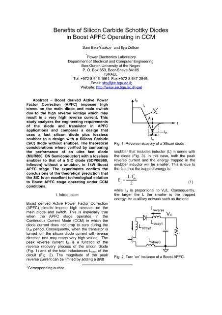
Benefits of Silicon Carbide Schottky Diodes in Boost APFC ...
Benefits of Silicon Carbide Schottky Diodes in Boost APFC ...
Benefits of Silicon Carbide Schottky Diodes in Boost APFC ...

You also want an ePaper? Increase the reach of your titles
YUMPU automatically turns print PDFs into web optimized ePapers that Google loves.
<strong>Benefits</strong> <strong>of</strong> <strong>Silicon</strong> <strong>Carbide</strong> <strong>Schottky</strong> <strong>Diodes</strong><br />
<strong>in</strong> <strong>Boost</strong> <strong>APFC</strong> Operat<strong>in</strong>g <strong>in</strong> CCM<br />
Sam Ben-Yaakov * and Ilya Zeltser<br />
* Power Electronics Laboratory<br />
Department <strong>of</strong> Electrical and Computer Eng<strong>in</strong>eer<strong>in</strong>g<br />
Ben-Gurion University <strong>of</strong> the Negev<br />
P. O. Box 653, Beer-Sheva 84105<br />
ISRAEL<br />
Tel: +972-8-646-1561; Fax:+972-8-647-2949;<br />
Email: sby@ee.bgu.ac.il;<br />
Website: http://www.ee.bgu.ac.il/~pel<br />
Abstract – <strong>Boost</strong> derived Active Power<br />
Factor Correction (<strong>APFC</strong>) imposes high<br />
stress on the ma<strong>in</strong> diode and ma<strong>in</strong> switch<br />
due to the high reverse voltage which may<br />
result <strong>in</strong> a very high reverse current. This<br />
study analyses the eng<strong>in</strong>eer<strong>in</strong>g requirements<br />
<strong>of</strong> the diode and transistor <strong>in</strong> <strong>APFC</strong><br />
applications and compares a design that<br />
uses a fast silicon diode plus lossless<br />
snubber to a design with a <strong>Silicon</strong> <strong>Carbide</strong><br />
(SiC) diode without snubber. The theoretical<br />
considerations where verified by compar<strong>in</strong>g<br />
the performance <strong>of</strong> an ultra fast diode<br />
(MUR860, ON Semiconductor) with a lossless<br />
snubber to that <strong>of</strong> a SiC diode (SDP06S60,<br />
Inf<strong>in</strong>eon) without a snubber, <strong>in</strong> 1kW <strong>Boost</strong><br />
<strong>APFC</strong> stage. The experiments confirm the<br />
conclusions <strong>of</strong> the theoretical prediction that<br />
the SiC is an excellent technological solution<br />
to <strong>Boost</strong> <strong>APFC</strong> stage operat<strong>in</strong>g under CCM<br />
conditions.<br />
I. Introduction<br />
<strong>Boost</strong> derived Active Power Factor Correction<br />
(<strong>APFC</strong>) circuits impose high stresses on the<br />
ma<strong>in</strong> diode and switch. This is especially true<br />
when the <strong>APFC</strong> stage operates <strong>in</strong> the<br />
Cont<strong>in</strong>uous Current Mode (CCM) <strong>in</strong> which the<br />
diode current does not drop to zero dur<strong>in</strong>g the<br />
D <strong>of</strong>f period. Consequently, when the transistor is<br />
turned 'on' the silicon diode current will reverse<br />
direction and may reach very high values. The<br />
peak reverse current I pk is a function <strong>of</strong> the<br />
reverse recovery process <strong>of</strong> the silicon diode<br />
(Fig. 1) and <strong>of</strong> the total <strong>in</strong>ductances L stray <strong>of</strong> the<br />
circuit (Fig. 2). The magnitude <strong>of</strong> the peak<br />
reverse current can be limited by add<strong>in</strong>g a di/dt<br />
I D<br />
I F<br />
V<br />
L<br />
t r<br />
Fig. 1. Reverse recovery <strong>of</strong> a <strong>Silicon</strong> diode.<br />
t rr<br />
snubber that <strong>in</strong>cludes <strong>in</strong>ductor (L) <strong>in</strong> series with<br />
the diode (Fig. 3). In this case, both the peak<br />
reverse current and the energy trapped <strong>in</strong> the<br />
snubber <strong>in</strong>ductor will be smaller. This is due to<br />
the fact that the trapped energy is:<br />
2<br />
L Ipk<br />
Et =<br />
2<br />
(1)<br />
while I pk is proportional to V o /L. Consequently,<br />
the larger the L the smaller is the trapped<br />
energy. An auxiliary network such as the one<br />
I reverse<br />
L stray1<br />
L stray2<br />
L stray3<br />
I pk<br />
V o<br />
Fig. 2. Turn 'on' <strong>in</strong>stance <strong>of</strong> a <strong>Boost</strong> <strong>APFC</strong>.<br />
t<br />
*Correspond<strong>in</strong>g author
L 3<br />
L 2<br />
L 1<br />
I pk<br />
I D<br />
I F<br />
Fig. 3. The effect <strong>of</strong> series <strong>in</strong>ductance on the<br />
reverse recovery process. L 3 > L 2 > L 1 .<br />
energy. An auxiliary network such as the one<br />
shown <strong>in</strong> Fig. 4 [2, 3] can recover this energy.<br />
Similar types <strong>of</strong> lossless snubbers have been<br />
used <strong>in</strong> the <strong>in</strong>dustry <strong>in</strong> recent years to remedy<br />
the adverse effects <strong>of</strong> the reverse recovery <strong>of</strong><br />
silicon diodes.<br />
The commercial <strong>in</strong>troduction <strong>of</strong> the <strong>Silicon</strong><br />
<strong>Carbide</strong> (SiC) <strong>Schottky</strong> diodes (Inf<strong>in</strong>eon)<br />
changes the pictures completely. As will be<br />
detailed <strong>in</strong> the paper, these fast diodes have<br />
negligible stored junction charge. Consequently,<br />
the reverse recovery current is very small and<br />
the behavior is more like a capacitor rather than<br />
the classical reverse recovery process found <strong>in</strong><br />
silicon diodes [1]. The objective <strong>of</strong> the study was<br />
to compare the performance <strong>of</strong> a fast silicon<br />
diode with lossless snubber, to that <strong>of</strong> a SiC<br />
diode <strong>in</strong> <strong>Boost</strong> <strong>APFC</strong> circuit, which is one <strong>of</strong> the<br />
most demand<strong>in</strong>g application.<br />
II. The Lossless Snubber<br />
The basic configuration <strong>of</strong> the lossless snubber<br />
applied <strong>in</strong> this study is given <strong>in</strong> Fig. 4 [3]. Its ma<strong>in</strong><br />
purpose is to limit the reverse recovery current<br />
and to recover the energy trapped <strong>in</strong> the<br />
snubb<strong>in</strong>g <strong>in</strong>ductor L s . At turn on <strong>of</strong> Q, L s limits<br />
di/dt and when the diode ceases to conduct the<br />
energy trapped <strong>in</strong> L s is moved to C s . At turn <strong>of</strong>f <strong>of</strong><br />
Q, D 1 ,D 2 clamp the dra<strong>in</strong> <strong>of</strong> Q to V o and the<br />
energy stored <strong>in</strong> C s is transferred first to L s and<br />
then to the output. Details are given <strong>in</strong> [3] which<br />
also discuss the tapped <strong>in</strong>ductor version <strong>of</strong> the<br />
snubber (Fig. 5). The purpose <strong>of</strong> the tap is to<br />
provide extra DC voltage to the resonant circuit<br />
so as to make sure that the ma<strong>in</strong> current will<br />
pass via D o dur<strong>in</strong>g T <strong>of</strong>f .<br />
S<strong>in</strong>ce the operation <strong>of</strong> the snubber relies on the<br />
proper operation <strong>of</strong> its resonant behavior, ample<br />
time must be given to the resonant process to<br />
complete. For example, if L s does not transfer all<br />
Fig. 4. Basic configuration <strong>of</strong> a <strong>Boost</strong> converter<br />
with lossless di/dt snubber.<br />
L <strong>in</strong><br />
n 1<br />
Q<br />
L s<br />
D<br />
C o<br />
s<br />
D 1<br />
D 2<br />
V o<br />
C o<br />
Fig. 5. Tapped <strong>in</strong>ductor version <strong>of</strong> the lossless<br />
snubber.<br />
the trapped energy to C s (just after the reverse<br />
recovery process) the current may build up,<br />
lead<strong>in</strong>g to a fault. Hence, the operation <strong>of</strong> the<br />
snubber relies on hav<strong>in</strong>g sufficient time for the<br />
process to complete dur<strong>in</strong>g turn on and turn <strong>of</strong>f.<br />
This leads to a restriction concern<strong>in</strong>g the<br />
m<strong>in</strong>imum permissible T on and T <strong>of</strong>f . The exact<br />
tim<strong>in</strong>g <strong>of</strong> the resonant cycle depends on the<br />
operat<strong>in</strong>g or conditions [2], but the order <strong>of</strong><br />
magnitude is approximately a quarter <strong>of</strong> the<br />
resonant period. i.e.<br />
π L C s s<br />
Tm<strong>in</strong><br />
≈<br />
2<br />
(2)<br />
The m<strong>in</strong>imums ON and OFF times restrict the<br />
permissible range <strong>of</strong> the duty cycle. The ma<strong>in</strong><br />
problem is the limitation <strong>of</strong> T <strong>of</strong>f that sets the limit<br />
for the maximum peak <strong>in</strong>put voltage. In <strong>Boost</strong><br />
converter:<br />
V o 1 =<br />
V<strong>in</strong><br />
D<br />
(3)<br />
<strong>of</strong>f<br />
And therefore:<br />
V<strong>in</strong> pk (max)= V o f s (1-T on (m<strong>in</strong>)) (4)<br />
Where f s is the switch<strong>in</strong>g frequency.<br />
L <strong>in</strong><br />
C s<br />
L s<br />
D 1 D 2<br />
D o<br />
V o<br />
t<br />
Q<br />
C o
This limitation is more significant as the switch<strong>in</strong>g<br />
frequency <strong>in</strong>creases. Consequently, if a high<br />
switch<strong>in</strong>g frequency is desired, either L s C S need<br />
to be made smaller. Mak<strong>in</strong>g the <strong>in</strong>ductor smaller<br />
will <strong>in</strong>crease the reverse recovery current and<br />
will <strong>in</strong>crease the voltage across C s just after turnon.<br />
This will <strong>in</strong>crease the reverse voltage <strong>of</strong> the<br />
output diode and may require a diode with a<br />
larger block<strong>in</strong>g voltage. Similarly, decrease <strong>in</strong> the<br />
value <strong>of</strong> C s will also <strong>in</strong>crease the voltage across<br />
it.<br />
An estimation <strong>of</strong> the practical limitations <strong>of</strong> the<br />
switch<strong>in</strong>g frequency can be obta<strong>in</strong>ed by the<br />
follow<strong>in</strong>g approximate analysis.<br />
The peak reverse current <strong>of</strong> the diode will be<br />
(Fig. 1):<br />
V<br />
I o<br />
pk = tr<br />
L<br />
(5)<br />
s<br />
Where t r is as def<strong>in</strong>ed <strong>in</strong> Fig. 1.<br />
The maximum voltage <strong>of</strong> the snubber capacitor<br />
(V C (max)):<br />
L<br />
V s<br />
C(max)<br />
= Ipk<br />
Cs<br />
or, by apply<strong>in</strong>g (5):<br />
VC<br />
(max) t<br />
= r<br />
Vo<br />
LsCs<br />
and from (2):<br />
VCc(max)<br />
πt<br />
= r<br />
Vo<br />
2Tm<strong>in</strong><br />
which implies<br />
πt<br />
T<br />
r<br />
m<strong>in</strong> ≈<br />
VC<br />
(max)<br />
2<br />
Vo<br />
(6)<br />
(7)<br />
(8)<br />
(9)<br />
An example <strong>of</strong> the constra<strong>in</strong>t imposed on the<br />
switch<strong>in</strong>g frequency we shall assume the<br />
follow<strong>in</strong>gs:<br />
V C (max)= M V o (10)<br />
1/T m<strong>in</strong> =P f s (11)<br />
where<br />
M, P < 1 (12)<br />
Us<strong>in</strong>g these def<strong>in</strong>itions:<br />
P M<br />
fs<br />
=<br />
π t<br />
(13)<br />
r<br />
Consider<strong>in</strong>g a practical case: t r =50nS; P=0.1;<br />
M=0.2, we f<strong>in</strong>d:<br />
f s ≈125kHz<br />
This numerical example clearly shows that the<br />
snubber technology is restricted to rather<br />
moderate switch<strong>in</strong>g frequencies. Higher<br />
switch<strong>in</strong>g frequencies can be reached by us<strong>in</strong>g<br />
faster diode, or us<strong>in</strong>g a diode with a higher<br />
breakdown voltage. Both will <strong>in</strong>crease the cost <strong>of</strong><br />
diode to be added to the extra components<br />
needed for implement<strong>in</strong>g the lossless snubber.<br />
III. The <strong>Silicon</strong>e <strong>Carbide</strong> <strong>Schottky</strong> Diode<br />
Unlike the case <strong>of</strong> a <strong>Silicon</strong>e diode, the <strong>Silicon</strong>e<br />
<strong>Carbide</strong> <strong>Schottky</strong> (SiCS) diode behaves more<br />
like a non-l<strong>in</strong>ear capacitor rather than a PN<br />
junction. That is, the charged energy <strong>in</strong> the SiCS<br />
is primarily a charge associated with a capacitor.<br />
Consequently, the diode’s turn-<strong>of</strong>f process<br />
entails a removal <strong>of</strong> a constant charge,<br />
practically <strong>in</strong>dependent <strong>of</strong> di/dt. The charge for a<br />
600V 6A diode is (SDP06S60, Inf<strong>in</strong>eon) is<br />
Q d =21nC for a forward current <strong>of</strong> 6Amp [4].<br />
Assum<strong>in</strong>g that all the energy associated with this<br />
charge is dissipated, the power loss due to this<br />
charge removed from the output V o at f s will be:<br />
P dq =Q d f s V 0 (14)<br />
At 100 kHz and 380V output voltage this would<br />
translate <strong>in</strong>to about 0.8W. However, as the<br />
frequency <strong>in</strong>creases, the dissipated power could<br />
be significant (8W at 1MHz). Conceivably, this<br />
charge could be circulated <strong>in</strong> a lossless manner<br />
by us<strong>in</strong>g a snubber similar to one shown <strong>in</strong> Fig.<br />
5. Assum<strong>in</strong>g that all energy is transferred to the<br />
snubber capacitor C s , the maximum voltage<br />
across it will be:<br />
V C (max)= Q d C s (15)<br />
For example, a 1nF capacitor will develop a<br />
21V voltage for the 21nQ charge, <strong>in</strong>creas<strong>in</strong>g only<br />
slightly the reverse voltage on ma<strong>in</strong> diode.<br />
However, to pursue this snubber idea for the<br />
SiCS diode at very high switch<strong>in</strong>g frequencies,<br />
one would need extremely fast diodes for D 1 , D 2<br />
(Fig. 4, 5). This approach was not pursued <strong>in</strong> this<br />
study.<br />
An additional po<strong>in</strong>t that needs to be mentioned is<br />
that the forward voltage drop <strong>of</strong> the SiCS diode<br />
is somewhat larger than that <strong>of</strong> the <strong>Silicon</strong>e
diode. Furthermore, the voltage drop <strong>in</strong>creases<br />
with junction temperature, opposite to behavior<br />
<strong>of</strong> the <strong>Silicon</strong>e diode. This <strong>in</strong>crease <strong>in</strong> voltage<br />
<strong>of</strong>fsets to some degree the reduction <strong>of</strong> switch<strong>in</strong>g<br />
losses. However, s<strong>in</strong>ce the power loss<br />
associated with the forward drop is not frequency<br />
dependent, the performance <strong>of</strong> the SiCS will be<br />
clearly superior to <strong>Silicon</strong>e diodes at very high<br />
switch<strong>in</strong>g frequencies.<br />
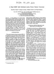
IV. Experimental Results<br />
The experiments were designed to compare the<br />
performance <strong>of</strong> an ultra fast diode (MUR860, ON<br />
Semiconductor) with a lossless snubber to that <strong>of</strong><br />
a SiC diode (SDP06S60, Inf<strong>in</strong>eon) without a<br />
snubber, <strong>in</strong> 1kW <strong>Boost</strong> <strong>APFC</strong> stage. The<br />
MUR860 is relatively slow as compared to<br />
recently <strong>in</strong>troduced super fast diodes that are<br />
more expensive. Output bus voltage was<br />
nom<strong>in</strong>ally 375V. The <strong>in</strong>put was 220VAC <strong>in</strong><br />
normal <strong>APFC</strong> operation or 155VDC when<br />
oscilloscope traces were recorded. Switch<strong>in</strong>g<br />
frequency was 120kHz. The power MOSFET<br />
was IRFP460. Snubber components (Fig. 5)<br />
were: L s = 7uH; C s =0.1uF; D 1 ,D 2 =MUR406; n=7.<br />
Fig. 6 shows the <strong>Silicon</strong>e diode and ma<strong>in</strong> switch<br />
currents at turn 'on', when the circuit was<br />
operated without a snubber. In this case, the<br />
output voltage was limited to 98V to prevent<br />
damage to the circuit. At turn 'on' the transistor<br />
carries the diodes current plus the <strong>in</strong>ductor<br />
current. Here the peak reverse current reached<br />
4Amp which implies that for 375V output the<br />
peak current would have reached 14Amp for the<br />
nom<strong>in</strong>al experimental forward current <strong>of</strong> 1.5Amp.<br />
The performance with the silicone diode and<br />
snubber is much better (Fig. 7), the maximum<br />
reverse current reached 3.8 Amp for the nom<strong>in</strong>al<br />
375V output. This peak is tolerable especially<br />
s<strong>in</strong>ce the snubber circulated the trap energy <strong>in</strong><br />
the <strong>in</strong>ductance.<br />
The performance <strong>of</strong> the SiC diode is superior to<br />
the silicone diode plus snubber solution (Fig. 8).<br />
Peak reverse current is less than the 2Amp<br />
(under same condition) and the reverse process<br />
is very short (less than 25nS).<br />
The study also exam<strong>in</strong>ed the switch<strong>in</strong>g process<br />
<strong>of</strong> the ma<strong>in</strong> switch with the silicon diode and<br />
snubber solution and when the SiC diode is<br />
used. In the case <strong>of</strong> the silicone diode with<br />
snubber, we f<strong>in</strong>d at turn-on a quick drop <strong>in</strong> the<br />
MOSFET voltage V DS (Fig. 9). The peak current<br />
reflects the peak reverse current <strong>of</strong> the diode. It<br />
should be noted though that at the <strong>in</strong>stance <strong>of</strong><br />
the peak, the dra<strong>in</strong> voltage is already low. In the<br />
SiCS diode case (no snubber) (Fig. 10), we<br />
Fig. 6. <strong>Silicon</strong> diode current (upper trace) and<br />
transistor current (lower trace) <strong>in</strong> <strong>Boost</strong><br />
<strong>APFC</strong> without snubber. V o = 98V;<br />
Horizontal scale: 50nS/div. Vertical<br />
scale: 2A/div.<br />
Fig. 7. <strong>Silicon</strong> diode current (upper trace) and<br />
transistor current (lower trace) <strong>in</strong> <strong>Boost</strong><br />
<strong>APFC</strong> with lossless snubber. V o =<br />
375V; Horizontal scale: 50nS/div.<br />
Vertical scale: 2A/div.<br />
Fig. 8. <strong>Silicon</strong> <strong>Carbide</strong> <strong>Schottky</strong> diode current<br />
(upper trace) and transistor current<br />
(lower trace) <strong>in</strong> <strong>Boost</strong> <strong>APFC</strong> with<br />
lossless snubber. V o = 375V; Horizontal<br />
scale: 50nS/div. Vertical sale: 2A/div.<br />
Fig. 9. MOSFET voltage and current when<br />
operated with <strong>Silicon</strong>e diode and a<br />
lossless snubber. Vertical scales:<br />
1A/div &100V/div. Horizontal scale:<br />
50nS/div.<br />
I<br />
DS<br />
V<br />
DS
V DS<br />
I DS<br />
Fig. 10. MOSFET voltage and current when<br />
operated with SiCS diode. Vertical<br />
scales: 1A/div &100V/div. Horizontal<br />
scale: 50Ns/div.<br />
Tplate, deg. C<br />
45<br />
40<br />
35<br />
30<br />
25<br />
20<br />
15<br />
10<br />
0 5 10 15 20 25<br />
P<strong>in</strong>, W<br />
Fig. 11. Heats<strong>in</strong>k calibration curve.<br />
observe a slower drop <strong>of</strong> the MOSFET voltage.<br />
This is due to the fact that the attenuat<strong>in</strong>g effect<br />
<strong>of</strong> L s is now absent. The peak voltage <strong>of</strong> the<br />
transistor is lower but, at the peak, the voltage <strong>of</strong><br />
the transistor is still relatively high. This process<br />
is a reflection <strong>of</strong> the fact that the energy loss<br />
associated with the average current due to the<br />
stored charge <strong>of</strong> the SiCs diode now dissipates<br />
<strong>in</strong> the transistor.<br />
The heats<strong>in</strong>k <strong>of</strong> the experimental set up was<br />
calibrated by the method detailed <strong>in</strong> [3]. It entails<br />
the measurement <strong>of</strong> the temperature rise as a<br />
function <strong>of</strong> the power dissipated by the devices<br />
attached to the heats<strong>in</strong>k. The calibration curve is<br />
shown <strong>in</strong> Fig. 11. Apply<strong>in</strong>g this procedure it was<br />
found that for a 350W power level the<br />
temperature rise for the case <strong>of</strong> <strong>Silicon</strong>e diode<br />
plus snubber and for the case <strong>of</strong> SiCs diode<br />
without snubber, was about the same: 32 o C. This<br />
corresponds to about 10W dissipation.<br />
V. Discussions and Conclusions<br />
The superior reverse recovery process <strong>of</strong> the<br />
SiCS diode which is characterized by short and<br />
small reverse current, eases the design <strong>of</strong> the<br />
<strong>Boost</strong> <strong>APFC</strong> stage. Losses will be lower and<br />
there is practically no need for a snubber to<br />
protect the circuit aga<strong>in</strong>st over-current and overvoltage<br />
peaks.<br />
This paper concentrated on the comparison<br />
between the SiCs diode and a (relatively slow<br />
and hence low cost) <strong>Silicon</strong>e diode plus a<br />
snubber. It is fair to assume that the SiCS<br />
technology will be more expensive than the<br />
silicone technology and hence a low cost<br />
<strong>Silicon</strong>e diode plus snubber may be comparable<br />
and even <strong>of</strong> lower price than the SiCS diode.<br />
Consequently, for switch<strong>in</strong>g frequencies <strong>of</strong> about<br />
100kHz, the SiCS may not have a significant<br />
advantage over the silicone diode. However, at<br />
higher switch<strong>in</strong>g frequencies the SiCS is no<br />
doubt a better choice both from the performance<br />
and economics po<strong>in</strong>ts <strong>of</strong> views.<br />
References<br />
[1] M. Bruckmann, E. Baudelot, B. Weis, and<br />
H. Mitichner, "Switch<strong>in</strong>g behaviour <strong>of</strong> diodes<br />
based on new semiconductor materials and<br />
silicon-a comparative study," EPE'97, 7th<br />
European Conference on Power Electronics<br />
and Applications, vol. 1, 513-17, 1997.<br />
[2] I. D. Jitaru, "S<strong>of</strong>t transitions power factor<br />
correction circuit," Proceed<strong>in</strong>gs <strong>of</strong> HFPC,<br />
202-208, May 1993.<br />
[3] H. Levy, I. Zafrany, I., G. Ivensky and Ben-<br />
Yaakov, S., “Analysis and evaluation <strong>of</strong> a<br />
lossless turn on snubber,” IEEE Applied<br />
Power Electronics conference, APEC-97,<br />
634-640, 1997.<br />
[4] Inf<strong>in</strong>eon Technologies AG,<br />
SDP/B06S60 data sheet, January, 2001.