A Dual IGBT Soft Switched Active Power Factor Corrector Sam Ben ...
A Dual IGBT Soft Switched Active Power Factor Corrector Sam Ben ...
A Dual IGBT Soft Switched Active Power Factor Corrector Sam Ben ...

You also want an ePaper? Increase the reach of your titles
YUMPU automatically turns print PDFs into web optimized ePapers that Google loves.
A <strong>Dual</strong> <strong>IGBT</strong> <strong>Soft</strong> <strong>Switched</strong> <strong>Active</strong> <strong>Power</strong> <strong>Factor</strong> <strong>Corrector</strong><br />
<strong>Sam</strong> <strong>Ben</strong>- Yaakov*, Gregory Ivensky, Vladimir Tantser, and Oleg Friedman<br />
Tel: +972- 7-6461561; Fax: +972- 7-6472949; Email: sby@bguee.bgu.ac.il<br />
<strong>Power</strong> Elecb"onics Laboratory<br />
Department of Electrical and Computer Engineering<br />
<strong>Ben</strong>-Gurion University of the Negev<br />
P. 0. Box 653, Beer-Sheva 84105, ISRAEL<br />
Abstract -A novel topology of an <strong>Active</strong> <strong>Power</strong><br />
<strong>Factor</strong> <strong>Corrector</strong> (APFC) based on a boost converter<br />
was studied theoretically and experimentally. The new<br />
design differs from previously described ones in the<br />
fact that it applies a <strong>Dual</strong> Switch <strong>Soft</strong> Switcher<br />
(DSSS) optimized for <strong>IGBT</strong>s. The main advantage of<br />
the DSSS is zero current switching of the main <strong>IGBT</strong><br />
and auxiliary <strong>IGBT</strong> during both turn on and turn off<br />
while all other power devices are also soft switched.<br />
The experimental 1 kW ac/dc APFC was run at a<br />
switching frequency of 66kHz. Theoretical and<br />
experimental results were found to be in good<br />
agreement. THD was estimated to be about 3%, the<br />
efficiency was measured to be about 96% .<br />
I. INTRODUcrlON<br />
The recently introduced fast and ultra fast <strong>IGBT</strong>s [I]<br />
are considered to be a cost effective choice in medium<br />
to high power applications. However, the relatively<br />
long turn-off time of these devices limit the switching<br />
frequency to about 25KHz. This limitation is<br />
especially noticeable in the single-switch active power<br />
factor correction circuit, in which the use of an <strong>IGBT</strong><br />
as the main switch could be highly beneficial.<br />
Consequently, the switching frequency limitation<br />
hampers the wide use of <strong>IGBT</strong>s in this class of<br />
applications which are presently of great commercial<br />
interest. This shortcoming could be corrected by a soft<br />
switching strategy that reduces the switching losses of<br />
the <strong>IGBT</strong>, permitting thereby efficient operation at<br />
high switching frequencies.<br />
The ideal arrangement for an <strong>IGBT</strong> soft switcher is<br />
Zero Current Switching (ZCS) or Zero Voltage<br />
Switching (ZVS) at turn on, but ZCS at turn off [2,3].<br />
ZCS at turn off is highly desirable since it can help<br />
remove the stored charge which otherwise might cause<br />
a long current tail. The recently introduced <strong>Dual</strong><br />
Switch <strong>Soft</strong> Switcher (DSSS) [4] meets these<br />
demands: it ensures soft switching during turn on and<br />
ZCS during turn off of the <strong>IGBT</strong>s while maintaining<br />
soft switching of all other power devi~s.<br />
The objective of this study was to'nvestigate the<br />
operation of a novel topology of an <strong>Active</strong> <strong>Power</strong><br />
<strong>Factor</strong> <strong>Corrector</strong> (APFC) based on a boost topology<br />
that differs from previously described ones [5] in the<br />
fact that a DSSS, optimized for <strong>IGBT</strong>s, is applied<br />
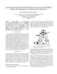
(Fig. I). The paper presents a theoretical analysis of<br />
operation of the DSSS, performance of the DSSS,<br />
design of a APFC stage with DSSS and experimental<br />
results of APFC with the DSSS.<br />
II. THE DUAL SWITCH TOPOLOGY AND<br />
ANAL YSIS OF ITS OPERA TION<br />
The <strong>Dual</strong> Switch <strong>Soft</strong> Switcher (DSSS) optimal for<br />
<strong>IGBT</strong>s is used in the boost converter (Fig. I). This<br />
switcher [4] includes two branches connected in<br />
parallel. The main switch Ql. shunted by an<br />
antiparallel diode Dl and connected in series with a<br />
resonant inductor Lr. forms the first branch. The<br />
second branch comprises the auxiliary switch Q2 in<br />
series with a diode DS. shunted by another antiparallel<br />
diode D2 and connected in series with a resonant<br />
capacitor Cr- The common point of Lr. Ql and Dl is<br />
clamped to the output of the converter through an<br />
auxiliary circuit which includes a Zener diode Dz and<br />
an ordinary diode D3. The common point of Cr. D2<br />
and DS is clamped to the output of the converter<br />
through a diode D4.<br />
The operation of DSSS is explained briefly as<br />
follows. The auxiliary switch Q2 is turned on just<br />
prior to the instant that the main switch Ql is due to<br />
be turned off. This creates a sinusoidal current in the<br />
series resonance network (Lr.Cr) which forces a<br />
negative current through the branch of the main switch<br />
(Ql.Dl). Consequently. Ql current reduces smoothly<br />
to zero whereupon the resonant current is channeled<br />
through the reverse diode Dl. When this diode is<br />
conducting. the gate drive of the main switch Ql can<br />
be removed under zero current conditions achieving<br />
thereby true ZCS. During 'turn on' of the main switch<br />
QI. the resonant inductor Lr ensures ZCS by limiting<br />
the rate of the current rise.<br />
The analysis of the DSSS was carried out under the<br />
following assumptions:<br />
1. The converter elements are ideal.<br />
* Corresponding author.
2<br />
2. The inductance of the main inductor Lin is large<br />
enough so that its current (the input current of the<br />
boost converter Iin) is practical constant during one<br />
switching cycle.<br />
3. The capacitance of the output capacitor Co is<br />
large enough so that the voltage across it (i.e. the<br />
output voltage of the convener Vo) can be considered<br />
constant during one switching cycle.<br />
These assumptions allow the use of an equivalent<br />
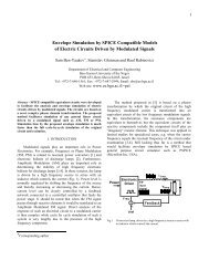
circuit of a boost convener with the DSSS (Fig. 2).<br />
Diodes D3. D4. D 5 and Dz are missing in Fig. 2<br />
because in ideal conditions (assumption 1) they are<br />
unnecessary. The practical function of these extra<br />
elements is described below (Section Ill).<br />
The operation of the DSSS will be discussed in<br />
relation to the waveforms of Fig. 3 that were obtained<br />
by PSPICE (MicroSim Inc.) simulations carried out<br />
under the above assumptions. Vgl and Vg2 are the gate<br />
voltages of the main (Ql) and auxiliary switch (Q2).<br />
The DSSS switching cycle includes seven stages<br />
(Fig. 3):<br />
1. In the interval preceding t 1 both transistors of the<br />
DSSS are 'off and the main diode of the converter Do<br />
is 'on'. The voltage of the main transistor Ql and<br />
capacitor Cr is Vo. This interval ends when the main<br />
transistor Ql is driven to turn on.<br />
2. In the interval tl-t2 the main transistor Ql and<br />
the main diode Do are conducting. As the current of<br />
Q 1 increases linearl y, the current of the diode Do<br />
decreases at the same rate since the sum of the two<br />
equals Iin. This commutation interval ends when the<br />
current of the main diode Do reaches zero and the diode<br />
Do turns off. The duration of the interval tl-t2 is<br />
found to be:<br />
3. Once the clamping effect of Do is removed, the<br />
resonant inductor Lr and resonant capacitor Cr are free<br />
to resonate. This resonant current will force the<br />
antiparallel diode Dl into conduction. That is, during<br />
the interval t2-t3 both the main transistor Ql and the<br />
antiparallel diode D2 of the auxiliary switch are<br />
conducting. They close the resonant path of Lr, Cr and<br />
carry the sinusoidal current that develops. The<br />
magnitude of the resonant current and the capacitor Cr<br />
voltage can be expressed as:<br />
if = IpkSin[ror(t-t2)] (2)<br />
VCr = Vocos[ror(t-tvJ (3)<br />
Fig. 2.<br />
Equivalent circuit of a boost converter with ideal<br />
<strong>Dual</strong> Switch <strong>Soft</strong> Switcher (DSSS).<br />
where:
-rc;<br />
Ipk = V°-V 1;<br />
(J)r = ~<br />
1<br />
(4)<br />
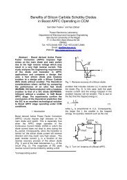
Vgl 1 : I : I: ~ ~ .. : : I I: I : I.<br />
~ :<br />
~<br />
~: : ;TA ; -~ : : : : I<br />
Vgl; ; : : I: : : : I ~<br />
VQ~<br />
I I I I I I I.<br />
I I. I I LA ~.<br />
I I. I I rllVo<br />
I I I I III<br />
i h~:pk<br />
~~.~i;n:<br />
Q K --:;==== ~~~ Im. ~<br />
.II I. III I.<br />
101<br />
:<br />
;<br />
:<br />
;<br />
:<br />
..-;<br />
: : ~~~k-<br />
;~ ;1.<br />
Iin ~<br />
-<br />
illi~ II ~ ~ Iinrl+-:--<br />
N I: : ~. I I: ~<br />
II I I I I I<br />
~ ~~: I : : I ::1~2VO V<br />
V~:,{~---ci1:;i~2VO<br />
"'<br />
,r I. .II I. 0<br />
vC ...<br />
tl: t3 : Time: t4 ~~-:-1Yo<br />
.I I<br />
t2<br />
t5 t7<br />
Fig. 3. Voltage and current waveforms of the DSSS in<br />
(5)<br />
the boost converter of Fig. 2 (simulation<br />
results).<br />
During this interval the current of the main switch<br />
(iQV supports two components: the main current (Iin)<br />
and the resonant current (ir):<br />
iQl = Iin + ir (6)<br />
This interval ends when the resonant current (ir)<br />
reaches zero and the antiparallel diode D2 turns off. At<br />
this instant, the capacitor Cr voltage is negative and<br />
equal, in its absolute magnitude, to the voltage Vo.<br />
The voltage on the main diode Do at this instant is<br />
equal 2Vo (Fig. 3).<br />
The duration of the interval t2-t3 is found to be:<br />
-r;-;:;- T r<br />
t2-3 = 7t"V LrCr = 2 (7)<br />
where T r is the resonant period.<br />
4. In the interval t3-t4 the main ~ansistOr QI is<br />
conducting while the auxiliary switch Q2 and all<br />
diodes are 'off .The voltage across the auxiliary switch<br />
Q2 and the main diode Do is V 0. This interval ends<br />
when the auxiliary switch Q2 is turned on. The<br />
voltage of the main diode Do swings at this moment<br />
to 2Vo.<br />
5. During the interval 14-t5 both transistors (QI and<br />
Q2) are conducting. They close the loop on the<br />
resonant circuit Lr, Cr , but now the resonant current<br />
ir is in the reverse direction compared to the interval<br />
t2-t3. Consequently, the current of the inductor Lr and<br />
the main switch Ql is now the difference between Iin<br />
and ir:<br />
iQl = Iin -ir (8)<br />
To secure ZCS, the peak resonant current Ipk (4)<br />
must be larger than Iin. If this condition is fulfilled,<br />
iQl will smoothly reach zero at an instant labeled t5.<br />
At this moment the antiparallel diode Dl will turn on.<br />
The duration of the interval 14-t5 is:<br />
14-5 = l.-gin-1F) (9)<br />
ror g'<br />
where:<br />
9 * (10)<br />
6. In the interval ts-l6 the auxiliary transistor Q2<br />
and the antiparallel diode Dl conduct The equivalent<br />
circuit is the same as in the interval 4 -ts .This<br />
interval ends when the diode (Dl) current smoothly<br />
reaches zero, turning it off. The duration of the interval<br />
ts-t6 is:<br />
2 1 1<br />
tS-6 = ~os- (-) (11)<br />
cor 9<br />
The gate drive of the main switch Ql must be<br />
removed during the interval ts-t6 and preferably at its<br />
beginning. The magnitude of the capacitor Cr voltage<br />
in the intervals t4-t6 can be expressed as:<br />
reaches<br />
VCr = -v ocos[o>r(t-t4)] (12)<br />
7. In the final operational stage l6-t7. the auxiliary<br />
transistor Q2 is conducting and all diodes are turned<br />
off. The capacitor Cr is charged under action of the<br />
current Iin. The interval ends when the voltage across<br />
the capacitor Cr (vCr )<br />
Vo and the main diode Do turns on. The<br />
duration of the interval t6-t7 is found to be:<br />
CrVn<br />
.t~-6<br />
16-7 = -':-" [1- sm(COr~)]<br />
Im 2<br />
The instant t7 marks the end of the complete<br />
switching cycle and the beginning of the next cycle.<br />
The gate drive of the auxiliary switch Q2 must be
4<br />
removed during the interval t7-(tl + T s) and preferable at<br />
its beginning. T s is the switching frequency period.<br />
The results of the above analysis, summarized in<br />
Table I, imply that both <strong>IGBT</strong>s and all diodes operate<br />
under soft switching conditions. The maximum<br />
voltage applied to the main Ql and to the auxiliary Q2<br />
transistor is equal V o while the maximum reverse<br />
voltage of the main diode Do is 2V 0.<br />
-.~ ~ .<br />
Transistor or Turn on Turn oh<br />
diode<br />
zcs<br />
zcs<br />
zvs<br />
zcs & zvs<br />
zcs & zvs<br />
zcs & zvs<br />
zcs & zvs<br />
zcs & zvs<br />
zcs<br />
zcs<br />
Table I. Switching conditions of the transistors and<br />
diodes.<br />
The converter voltage ratio ~ v. is derived as a<br />
In<br />
function of the apparent duty cycle (Da> defined as:<br />
TL\<br />
Da = -:r; (15)<br />
where TL\ = tl-4<br />
is the time interval between tl when<br />
the main switch (Ql) is turned on and 4 when the<br />
auxiliary switch (Q2) is turned on (Fig. 3); T s is the<br />
switching period.<br />
The voltage transfer ratio is obtained by applying<br />
the assertion that in steady state the average voltage<br />
across the main inductor Lin must be zero, i.e.:<br />
Ts<br />
IVLdt = O (16)<br />
O<br />
where vL is the instantaneous value of the voltage<br />
across the main inductor Lin (in the equivalent circuits<br />
of Fig. 2 VL is the voltage across the current source<br />
lin).<br />
In the intervals t2-t3 and 4-17<br />
vL = Vin -vC (17)<br />
in the interval t3-4<br />
VL = V in (18)<br />
and in the intervals tl-t2 and 17-(tl + T s)<br />
VL=Vin- Vo (19)<br />
We assume:<br />
1. The duration of the interval tl-t2 is negligible<br />
small.<br />
2. The capacitor voltage vC in the interval t6-17 is<br />
described by equation (12) instead of (13). That is, the<br />
duration of the interval 4-17 can be Clpproximated by<br />
:!:r ,<br />
2.<br />
Inserting (17) -(19) in (16) and applying (3), (7),<br />
~-<br />
v<br />
T<br />
'8--- 1<br />
V. -Tr -I-De<br />
m T8-(T~+2)<br />
where De is the equivalent duty cycle defmed by:<br />
Tr<br />
De = Da + ~ c--o\~ Tr<br />
= T s {:ll)<br />
.<br />
That is, the equivalent duty cycle De includes two<br />
terms: the fIrst one is the apparent duty cycle Da (15)<br />
and the second one represents the resonant transition.<br />
The minimal value of the apparent duty cycle Da min<br />
(for proper operation) corresponds to the case when the<br />
auxiliary switch Q2 is turning on at the same instant<br />
when the antiparallel diode D2 turns off, i.e. when<br />
t3-t4 = 0. In this case<br />
T<br />
T~ = t3-1 = t3-2 = ¥<br />
That is, the minimum apparent duty cycle Da min is:<br />
Tr<br />
Da min = ~ (22)<br />
and the corresponding minimal value of the equivalent<br />
duty cycle is expressed as:<br />
Tr Tr fs<br />
De min = Da min + ~ = T; = C; (23)<br />
The maximum value of the equivalent duty cycle<br />
will approach unity under the assumption, made<br />
above, that the interval 11-12 (Fig. 3) is negligibly<br />
small. A more rigorous analysis shows that if 11-12 is<br />
considered, than the more accurate upper bound to the<br />
equivalent duty cycle (De max ) is:<br />
tl-2<br />
De max = I -~ (24)<br />
or, applying (1), (4), (5), (7), and (10)<br />
De max = I -- Tr<br />
fs<br />
2 T = I --<br />
2 f (25)<br />
7tg s 7tg r<br />
The maximal value of the apparent duty cycle can be<br />
defined from the approximate equation:<br />
Da max = I -~<br />
Tr<br />
(26)<br />
The average current of the main transistor IQ I av<br />
can be described by the following approximated<br />
equation [4]:<br />
IQl av = Iin (Da + -gTr<br />
7t<br />
T ) (27)<br />
s<br />
As would be expected, the average current of the main<br />
transistor is higher than in conventional hard switched<br />
PWM conveners (where IQl av = D Iin). But if Tr<br />
(the resonance period) is much shorter than T s and<br />
g=Ipk/Iin is relatively small (g=I.3 ...1.5) the penalty<br />
paid for ZCS will be rather negligible.<br />
III. PERFORMANCE<br />
OF THE DSSS<br />
(11), (12) and (15) we find: The analysis given above describes the operation of<br />
an ideal DSSS. However, turn 9ff processes in
5<br />
practical transistors and diodes may affect the opemtion<br />
of real DSSS switcher. In particular, a mpid reverse<br />
recovery of diode Dl when it turns off will induce a<br />
high voltage on the inductor Lr and therefore across the<br />
main transistor Ql. This will initiate parasitic<br />
oscillations in the resonant network which includes<br />
inductor Lr, the capacitances of the turned off diode Dl<br />
and the turned off transistor Ql. This undesired<br />
situation can be corrected by clamping the common<br />
point of the inductor Lr, the main transistor Ql and<br />
the antiparallel diode Dl to voltage source Vo through<br />
an auxiliary circuit which includes a Zener diode Dz<br />
and an ordinary diode D3 (Fig. 1). In this case the<br />
transistor voltage vQ 1 will be limited to V 0+ V Z ,<br />
where Vz is the breakdown voltage of Dz.<br />
The function of the Zener diode is to help reduce to<br />
zero any residual currents in Lr (such as the reverse<br />
recovery current of Dl) after the main switch (Ql) is<br />
turned off. Without the Zener diode, the current of the<br />
inductor Lr will continue to flow through D3<br />
increasing overall losses and causing hard switching<br />
of Ql at turn on.<br />
The pmctical switcher (Fig. 1) includes an additional<br />
diode (D4) that clamps the auxiliary transistor (Q2) to<br />
the voltage source Vo to protect Q2 against voltage<br />
spikes generated by stray inductances. An additional<br />
diode (D5) is used to reduce the collector capacitance of<br />
(Q2) and hence helps to suppress parasitic oscillations.<br />
The experimental converter with DSSS (Fig. 1) had<br />
the following parameters:<br />
IV. DESIGN OF A lKW APFC STAGE AND ITS<br />
EXPERIMENTAL INVESnGA nON<br />
The design of a practical DSSS-based APFC has<br />
to address several unique subjects:<br />
I. Generation of two gate signals, one for the main<br />
switch and one for the auxiliary switch.<br />
2. Timing of the gate signals in terms of the delay<br />
between them and the length of the auxiliary<br />
<strong>IGBT</strong> gate signals.<br />
3. Ensuring a minimum 'turn on' duration of the<br />
main switch so as to make sure that the resonant<br />
cycle comes to an end. If not, the resonant<br />
capacitor Cr will not charge to a sufficient<br />
voltage level as required for driving the resonant<br />
network during the 'turn off instance.<br />
Furthermore interruption of the resonant current<br />
may cause high voltage spikes on the switches.<br />
4. Setting a limit to the maximum apparent duty<br />
cycle so as to ensure a minimum 'turn off time<br />
necessary for the resonant cycle at 'turn off to<br />
come to an end.<br />
5. Specifying the current and voltage ratings of the<br />
extra components of the DSSS.<br />
180V AC input; 380V output; lkW; switching<br />
frequency = 66kHz; Lin -1.2mH; Lr -22~H; Cr -<br />
10.6nF; Ql, Q2 -IRGBC20U; Do -MUR8100; Di,<br />
D2, D3 -MUR450; D4 -MUR460; D5 -MBR1305;<br />
Dz -5V Zener.<br />
Experimental investigation was carried out in two<br />
stages. The operation conditions of DSSS in a DC-DC<br />
boost converter were examined fIrstly. Experimental<br />
voltage and current waveforms (Fig. 4) were found to<br />
be smooth and practically identical to the theoretical<br />
waveforms depicted in Fig. 3, except for the trench<br />
that follows the peak current of main switch current<br />
(QV. The deep is attributed to the reverse recovery of<br />
the antiparallel diode D2. This deviation from the<br />
theoretical waveform has only a slight affect on the<br />
operation of the switcher: it reduces somewhat the<br />
maximum voltage on Cr (by about 10%). This, in<br />
turn, reduces the maximum peak current during turn<br />
off commutation.<br />
.Res.ults. of th~ sec~nd stage of th\ exper~mental<br />
mvesugauon (With acuve power factorcorrecuon) are<br />
given below (see Section IV).<br />
Fig. 4. Experimental waveforms of the main switch<br />
voltage vQ 1 and current iQ. Vertical scales:<br />
200V/div, 5Ndiv.<br />
Horizontal scale 2~S/div.<br />
In the design presented here, the operation was based<br />
on Continuous Current Mode (CCM) which is more<br />
suitable for high power levels. The borderline<br />
Discontinuous Current Mode (DCM) -CCM method<br />
[5] has no advantage over the DSSS which provides<br />
soft switching as does the DCM-CCM approach.<br />
However CCM has lower peak current and hence rms<br />
current which improves efficiency and therefore more<br />
appropriate to higher power levels.
6<br />
+15 v~<br />
Gate signal<br />
~ I<br />
from UC3854<br />
The control of the APFC explored in this study,<br />
was based on a conventional APFC controller to<br />
which some circuitry was added. The present design<br />
applied a Unitrode UC3854 IC unit, but any other<br />
CCM controller will equally do.<br />
The initial problem that had to be overcome is the<br />
generation of the two gate signals required for the<br />
DSSS, out of the single gate output of the controller.<br />
The two gate signals are obtained by passing the<br />
controller's gate-drive signal through a simple logic<br />
processor that is built around conventional gates (Fig.<br />
5). Overlapping between the main switch gate control<br />
and the auxiliary gate control is achieved by stretching<br />
the original PWM signal of the controller with the<br />
signal generated by the monos table built around gates<br />
lA and IB (Figs 5 & 6). A delay circuit, built around<br />
gate B is then used to generate the auxiliary pulse<br />
which is longer than the stretched portion of the main<br />
gate signal. Finally, an additional delay circuit (built<br />
around 2B, 2A and 2C) is used to set the minimum<br />
pulse width of the main switch control. The fact that<br />
the controller's PWM signal is stretched, does not<br />
harm the feedback loop since the current error amplifier<br />
of the controller will automatically adjust the pulse<br />
width so that the total duration (original pulse plus<br />
stretched portion) will be as required for any given<br />
operating point. The fact that the minimum duty cycle<br />
is clamped to a pre-set value does not affect operation<br />
as long as the input voltage is sufficiently lower than<br />
the output voltage. When the peak input voltage<br />
approaches that of the output (and calls~or a duty cycle<br />
below Dmin set by the logic processor) the converter<br />
will enter an interrupted mode that is, cycling between<br />
operation and lock-out periods.<br />
G d .I I<br />
aIC nve<br />
from Uc!i85A~ Toff,.r--l I<br />
JUJ~ Ion I I I I ><br />
I I I t<br />
2C outp;;l , Ton ~ r=:J ~ switch driver)<br />
J; ITofr I I I ><br />
I I<br />
A ou~ (to a~h driver)<br />
.I ~ -I Toff -I I ~<br />
I<br />
Fig. 6. Gate voltages of the main and auxiliary switches<br />
of the DSSS.<br />
The problem of limiting the maximum duty cycle<br />
to a safe value (see point 4 above) was solved by<br />
clamping the output of the error amplifier of the<br />
APFC controller (pin 5 in the case of UC3854) to a<br />
voltage level that corresponds to the maximum duty<br />
cycle (0.9 in the experimental unit). The limitalion of<br />
the maximum duty cycle will cause some distortion<br />
around zero current crossovers. This is found, however,<br />
even in conventional APFC controllers which are<br />
normally limited to some maximum duty cycle.<br />
Furthennore, other effects, such as the nonlinearity of<br />
the input rectifiers (Fig. I) and hence the distorted<br />
input current reference, are probably more influential<br />
on input current distortion around the zero crossing<br />
region.<br />
t<br />
t
7<br />
The design details of the APFC stage were as<br />
described above (Section III). The resonant components<br />
were chosen to withstand the expected operational<br />
conditions. The rms current of the resonant inductor Lr<br />
is, to a fIrst approximation, equal to the main inductor<br />
current while the peak current is about twice that of<br />
the main inductor current. The resonant inductor was<br />
wound on a ferrite pot-core structure with an air gap.<br />
Although the rms current of the resonant capacitor (Cc)<br />
is moderate, the peak current is high twice the<br />
maximum input current. This necessitate the selection<br />
of a high current capacitor (polypropylene was chosen<br />
in the present case). The purpose of the input capacitor<br />
Cin (0.22 ~ is to confine the high frequency ripple<br />
to the converter side of the mains rectifiers (Fig. 1).<br />
The experimental waveform of input line current<br />
practically coincides with line voltage (Fig. 7). It<br />
should be noticed that the THD of the line voltage in<br />
our laboratory is rather poor, about 7%. Due to the<br />
lack of a pure AC source no direct measurements of<br />
lliD were possible. Comparison of the line and input<br />
current nIDs yield a nID estimate for the line current<br />
of about 3%. The efficiency was measured to be about<br />
96% at the power level range of 370W to 900W. The<br />
output characteristic of the experimental prototype is<br />
almost horizontal (Fig. 8). The drop, typical to this<br />
APFC topology, is due to the finite gain of the outer<br />
(voltage) feedback loop.<br />
Fig. 7. Experimental waveforms of the rectified line<br />
voltage v line and line current iline. Vertical<br />
scales: 80V /div .0.7 A/div .Horizontal scale<br />
5mS/div.<br />
Fig. 8. Output characteristic of the experimental<br />
converter with APFC.<br />
v. CONCLUSIONS<br />
This study demonstrated two important facts:<br />
-the DSSS topology can be easily implemented in<br />
practical APFC circuits;<br />
-by applying the DSSS approach, one can operate<br />
<strong>IGBT</strong>s at a rather high frequency without a noticeable<br />
penalty in power losses.<br />
The proposed soft switched APFC appears to offer<br />
an improvement to APFC designs.<br />
REFERENCES<br />
[1] T. Tsunoda, M. Hideshima, M. Kuwahara, T.<br />
Kuramoto, and A. Nakagawa, "Improved 600 and<br />
1200 V <strong>IGBT</strong> with low turn-off loss and high<br />
raggedness", Proceedings of APEC'90. pp. 9-<br />
16.<br />
[2] R. Rangan, D. Chen, J. Yang, and J. Lee,<br />
" Application of insulated gate bipolar transistor<br />
to zero-current switching converters", IEEE<br />
Transactions on <strong>Power</strong> Electronics. Vol. 4, No.<br />
1, January 1989, pp.2-7.<br />
[3] K. Chen, and T. A. Stuart, "A study of <strong>IGBT</strong><br />
turn-off behavior and switching losses for zerovoltage<br />
and zero current switching", Proceedings<br />
of APEC'92, pp.411-418.<br />
[4] G. Ivensky, D. Sidi, and S. <strong>Ben</strong>-Yaakov, "A soft<br />
switcher optimized for <strong>IGBT</strong>s in PWM<br />
topologies", Proceedings of APEC'95, pp.900-<br />
906.<br />
[5] R. A. Mammano, "New developments in high<br />
power factor topologies", Proceedings of<br />
HFPC'96, pp. 63- 74.<br />
,