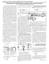
Envelope Simulation by SPICE Compatible Models of Electric ...
Envelope Simulation by SPICE Compatible Models of Electric ...
Envelope Simulation by SPICE Compatible Models of Electric ...

You also want an ePaper? Increase the reach of your titles
YUMPU automatically turns print PDFs into web optimized ePapers that Google loves.
1<strong>Envelope</strong> <strong>Simulation</strong> <strong>by</strong> <strong>SPICE</strong> <strong>Compatible</strong> <strong>Models</strong><strong>of</strong> <strong>Electric</strong> Circuits Driven <strong>by</strong> Modulated SignalsSam Ben-Yaakov * , Stanislav Glozman and Raul RabinoviciDepartment <strong>of</strong> <strong>Electric</strong>al and Computer EngineeringBen-Gurion University <strong>of</strong> the NegevPOB 653, Beer-Sheva 84105, IsraelTel: +972-7-646-1561; Fax: +972-7-647-2949; Email: s<strong>by</strong>@ee.bgu.ac.ilWeb site: www.ee.bgu.ac.il/~pelAbstract - <strong>SPICE</strong> compatible equivalent circuits were developedto facilitate the analysis and envelope simulation <strong>of</strong> electriccircuits driven <strong>by</strong> modulated signals. The circuits are based ona novel complex phasor domain transformation. The proposedmethod facilitates simulation <strong>of</strong> any general linear circuitdriven <strong>by</strong> a modulated signal such as AM, FM or PM.<strong>Simulation</strong> time <strong>by</strong> the proposed envelope simulation is muchfaster than the full cycle-<strong>by</strong>-cycle simulation <strong>of</strong> the originalcircuit and excitation.I. INTRODUCTIONModulated signals play an important role in PowerElectronics. For example, Frequency or Phase Modulation(FM, PM) is related to resonant power converters [1] andelectronic ballasts <strong>of</strong> discharge lamps [2]. Furthermore,Amplitude Modulation (AM) plays an important role indetermining the stability <strong>of</strong> high frequency electronicballasts for discharge lamps [3,4]. In these systems, the lampis driven <strong>by</strong> a high frequency source in series with aninductor which controls the current (Fig. 1). Power level isnormally regulated <strong>by</strong> shifting the frequency <strong>of</strong> the sourceand there<strong>by</strong> increasing or decreasing the current. Hence,current level can be closely controlled <strong>by</strong> a feedbacknetwork connected to a controlled oscillator that feeds thepower stage. It should be noted that when the FM signalpasses through reactive elements it would be translated to anAmplitude Modulated FM signal. Direct analysis <strong>of</strong> theresponse <strong>of</strong> such an electrical circuit to a modulated carrieris thus complex while cycle <strong>by</strong> cycle simulation <strong>of</strong> such asystem is very lengthy due to the presence <strong>of</strong> the highfrequency component.The method proposed in [5] is based on a phasortransformation <strong>by</strong> which the original circuit <strong>of</strong> the highfrequency modulated carrier is transformed into anequivalent circuit <strong>of</strong> the low frequency modulation signals.In this transformation, the resistance components areequivalent to themselves but the equivalent circuits <strong>of</strong> thereactive components include the component itself plus an''imaginary'' resistor element. This technique was applied inlimited studies for specialized cases, e.g. when the carrierfrequency equals the resonant frequency <strong>of</strong> the circuit underexamination [3,4]. Still lacking thus far is a method thatwould facilitate envelope simulation <strong>by</strong> <strong>SPICE</strong> basedgeneral purpose circuit simulator such as P<strong>SPICE</strong>(MicroSim Inc. USA).3RZHUFig. 1.(OHFWURQLF'ULYHUFreqΣ 9UHIFMinputsignalFeedback, lamp9 lampFluorescent lamp, driven <strong>by</strong> a high frequency source in series withan inductor which controls the current.* Corresponding author
2In this study we developed a complex phasortransformation approach that was then used to derive a<strong>SPICE</strong> compatible model transparent to the high frequencycarrier. The proposed method facilitates envelope simulation<strong>of</strong> any linear electric circuits <strong>by</strong> any general purposesimulator. This approach differs from earlier solutions toenvelope simulation which rely on specialized computerprograms [6].II. COMPLEX PHASOR TRANSFORMATIONAPPROACHAny analog modulated signal (AM, FM or PM) can bedescribed <strong>by</strong> the following general expression:u(t)= U1(t)⋅cos(ωct)+ U 2 (t) ⋅sin(ωct) (1)where U1(t) and U 2(t) are the modulation signals and ω c isthe angular frequency <strong>of</strong> the carrier.Expression (1) could also be written as:or as:u(t)= Re[(U1(t)− j⋅U 2 (t)) ⋅exp(jωct)] (2)[ exp(arg(U(t)) ⋅exp(jωt) ]u(t)= U(t) ⋅ Rec (3)−1⎛ − U ⎞where 'arg(U(t))' is⎜ 2 (t)tan⎟ .⎝ U1(t)⎠Expression (3) implies that the modulated signal in thetime domain u(t) can be represented <strong>by</strong> a generalized phasorthat both its magnitude and phase are time dependent. Theexpression <strong>of</strong> the complex phasor U &(t)is:&U(t)= U1(t)− jU 2 (t)The magnitude:&2 2 1/ 2U (t) = [U1 (t) + U 2 (t)]is equal to the modulation envelope <strong>of</strong> the original signalu(t) (eq. (3)).As will be shown next, the complex phasor&representation U(t)= U1(t)− jU 2 (t), introduced here, canbe used to drive the low frequency equivalent circuits thatrepresent the envelope behavior <strong>of</strong> the system withoutinvolving the high frequency carrier. This would shortensimulation time considerably since the time domain analysisdoes not include the high frequency component. Theequivalent circuit is obtained similar to [6] <strong>by</strong> a phasortransformation <strong>of</strong> the electric components L, C, and R. Aninductor L in the original circuit becomes an inductive(4)(5)component L in series with an imaginary resistor jω c L in theequivalent circuit, a capacitive component C becomes acapacitor C in parallel to an imaginary resistor 1/(jω c C), anda resistor component R is equivalent to the same resistorcomponent R. Therefore, the equivalent circuit in thegeneralized phasor domain will consist <strong>of</strong> inductors,capacitors, and resistors in series or in parallel to''imaginary'' resistors. Such a circuit is not compatible with<strong>SPICE</strong> simulators and consequently an additionaltransformation is needed to permit simulation <strong>by</strong> commoncircuit simulators. This additional step is described in thefollowing section.III. <strong>SPICE</strong> MODELS FOR CIRCUITS WITHIMAGINARY RESISTORSThe proposed methodology is demonstrated <strong>by</strong>considering an L, R circuit (Fig. 2a) driven <strong>by</strong> a generalizedmodulated signal:v(t)= V1 (t) cos( ωct)+ V2(t) sin( ωct)(6)The equivalent circuit in the generalized phasor domain(Fig. 2b) can be described <strong>by</strong>:&& & dI(t) &V(t)= RI(t) + L + jωcLI(t)(7)dtYW9M9 5i(t)(a)5 /(b)5 /9 I ,M, 5 /9 I (c)/j*ωc*L-I*ωc*LI *ωc*LFig. 2. <strong>SPICE</strong> model for a circuit with an ''imaginary'' resistor: (a) originalR, L circuit driven <strong>by</strong> a modulated voltage source; (b) theequivalent circuit <strong>of</strong> (a) in the generalized phasor domain; (c) crosscoupled equivalent circuits based on (11) and (12) that replace (b).
3where the last term could be interpreted as an "imaginary"resistor <strong>of</strong> the 'value' jωcL. V & &(t)and I(t)are the complexphasors that prevail in the equivalent circuit <strong>of</strong> Fig. 2b:&V(t)= V 1(t)− jV2(t)&I(t)= I1 (t) + jI2(t)Applying (8) and (9), (7) can be rewritten as:V1− jV2= R(I1+ jI 2 ) +d(I1+ jI 2 )+ L + jωcL(I1+ jI 2 ) (10)dtTo facilitate analysis <strong>by</strong> general purpose circuitsimulators we divide the complex equation (10) into real andimaginary parts:dI1V1 RI1+ L − ωcLI2dtdI2− V2 = RI2+ L + ωcLI1dt(8)(9)= (real) (11)(imaginary) (12).The two equations, (11) and (12), can now be emulated<strong>by</strong> two interconnected circuits (Fig. 2c). Notice that thisrepresentation does not involve imaginary resistors and thatlast terms in (11) and (12) are emulated <strong>by</strong> cross-coupleddependent voltage sources (a voltage source whosemagnitude is a linear function <strong>of</strong> the current in the crosscircuit). The newly developed equivalent circuits <strong>of</strong> Fig. 2ccontain only conventional electric components and aretherefore <strong>SPICE</strong> compatible. A similar but dual thinking canbe followed for a capacitor in parallel with the ''imaginary''resistor. For example, the equations for a capacitor C inparallel to a conductance G, fed <strong>by</strong> a current sourcemodulated signal, will be:dV1I1 GV1+ C − ωcCV2dtdV2I2 = GV2+ C + ωcCV1dt= (real) (13)− (imaginary) (14)Following this approach, <strong>SPICE</strong> compatible circuitscould be developed for more involved circuit configurations.The usefulness <strong>of</strong> the proposed simulation method isfurther demonstrated <strong>by</strong> considering the case <strong>of</strong> phasemodulated (PM) voltage source driving the circuit <strong>of</strong> Fig. 2a.The source is assumed to be <strong>of</strong> the form:v(t)= A cos[ ωct+ m p sin( ωmt)](15)Therefore, the equivalent circuit <strong>of</strong> Fig. 2b is driven <strong>by</strong>the generalized voltage phasor:&V(t) = A cos[m p sin( ωmt)] ++ jA sin[m p sin( ωmt)](16)Consequently, the <strong>SPICE</strong> compatible equivalent circuits<strong>of</strong> Fig. 2c are driven <strong>by</strong> the sourcesV1 = A cos[m p sin( ωmt)](17)− V2 = A sin[m p sin( ωmt)](18)The circuits <strong>of</strong> Fig. 2c were fed to a P<strong>SPICE</strong> simulator(evaluation version 8) via the Schematics Capture front end<strong>by</strong> using the appropriate symbols (dependent voltage sourceare represented <strong>by</strong> EVALUE symbols). The simulation wasrun for the following values: R= 10Ω, L= 7 mH, A= 200V,f c = ωc/2π= 40kHz, m p = 10, f m = ωm/2π =2kHz.Fig. 3a shows the original current i through the circuit<strong>of</strong> Fig. 2 (upper trace) and the envelope <strong>of</strong> the current,obtained <strong>by</strong> the circuits <strong>of</strong> Fig. 2c and applying (5) (lowertrace). Fig. 3b compares the results <strong>of</strong> cycle <strong>by</strong> cyclesimulation and envelope simulation. Fig. 3c depicts thevoltage phasor components V 1 and -V 2 , while Fig.3d thecurrent phasor components I 1 and I 2 . The spectrum <strong>of</strong> thecurrent <strong>of</strong> the original circuit (Fig. 2a) is shown in Fig. 4awhile the spectrum <strong>of</strong> the reconstructed current is given inFig. 4b. The reconstruction was calculated <strong>by</strong>:i(t)= I1(t) cos( ωct)+ I 2 (t) sin( ωct)(19)applying the original carrier frequency and the envelopecomponent (I1, I2) <strong>of</strong> the <strong>SPICE</strong> simulation results based onFig. 3c. It is evident that both the envelope signals (Fig. 3)and the spectra (Fig. 4) obtained <strong>by</strong> the proposed simulationmethod are identical to the original ones.IV. THE GENERAL CASEConsider a general R, L, C circuit that is driven <strong>by</strong> amodulated carrier u(t). The matrix state space equation <strong>of</strong> thesystem is:x = A ⋅ x + B ⋅ u(20)By expressing u as the complex excitation (4), insertingit in (20) and breaking the resulting complex state spaceequation into real and imaginary parts one obtains: (21)X1 = A ⋅ X1− A1⋅ X 2 + B⋅U1 (22)X 2 = A ⋅ X 2 + A1⋅ X1− B⋅U 2where X1, X2 are the complex state variables <strong>of</strong> the phasordomain circuit, U1, U2 are the source complex phasors and
4P$P$(a)$P$$P$(b)$PVPV7LPHPV$N+]N+])UHTXHQF\N+]P$(a)Fig. 4. Signal spectra: (a) current in the original circuit (Fig. 2a); (b)reconstructed current spectrum . See text for details.P$$99 9PV7LPH(b)PVPVA1 is the matrix <strong>of</strong> the imaginary resistors, jωcL associatedwith each inductor and 1 jω cCassociated with eachcapacitor (ωc is the carrier frequency). The cross coupledterms A1X2 in (21) and A1X1 in (22) can be represented asdependent sources: voltage source in the inductor case andcurrent source for the capacitor case. Original resistors areleft as is. Equations (21) and (22) can now be simulated astwo circuits that include dependent sources that are afunction <strong>of</strong> the state variables <strong>of</strong> the cross circuits. Note that(21) and (22) include only the low frequency componentwhile the high frequency carrier is present only as analgebraic coefficient (ωc).999 99P$, $P$P$PVPV7LPH(c), $P$PVPV7LPH(d)PVPVFig. 3. <strong>Simulation</strong> results on the circuit <strong>of</strong> Fig. 2: (a) current i through theoriginal circuit <strong>of</strong> Fig. 2a (upper trace) and envelope <strong>of</strong> the current,obtained <strong>by</strong> envelope simulation based on Fig. 2c (lower trace); (b)traces (a) zoomed and superimposed; (c) voltage phasorcomponents V 1and -V 2; (d) current phasor components I 1and I 2.V. IMPLEMENTATIONPreparation <strong>of</strong> (21) and (22) for analysis <strong>by</strong> generalpurpose analog circuit simulator can proceed <strong>by</strong> translatingthe equations into equivalent circuits. Matrix 'A' is that <strong>of</strong> theoriginal circuit, whereas ' A 1' is new matrix representing thecoupled dependent sources. Here we describe a directmethod that <strong>by</strong>passes the need for constructing the newmatrix. Starting with a general R, L, C circuit (Fig. 5a) thatis driven <strong>by</strong> a modulated carrier v(t), we first replace thereactive elements <strong>by</strong> dependent sources. An inductor Li isreplaced <strong>by</strong> a current source i Li and a capacitor Ci isreplaced <strong>by</strong> a voltage source v Ci (Fig. 5b). The magnitude<strong>of</strong> the dependent sources is linked to auxiliary circuits thatemulate the behavior <strong>of</strong> the elements. That is, the auxiliarycircuit for Li comprises a dependent voltage source v Li thatforces the in-circuit voltage on the inductor Li. The currentgenerated in the auxiliary circuit is then fed back to the maincircuit <strong>by</strong> the dependent current source i Li that representsthe inductor. In a similar way, dependent voltage sourcesv Ci replace capacitors in the main circuit. This separationstep is not crucial but is used to streamline the structure <strong>of</strong>the equivalent circuits that will later evolve and allowautomatization <strong>of</strong> the process.
5Fig. 5.Derivation <strong>of</strong> phasor equivalent circuits. (a) Original circuit. (b)Replacing reactive elements <strong>by</strong> dependent sources. (c) Real part <strong>of</strong>phasor equivalent circuit. (d) Imaginary part <strong>of</strong> phasor equivalentcircuit.The next step applies the transformation <strong>of</strong> the circuitinto two phasor circuits per (21) and (22). Now we apply thetwo phasor sources V 1 and − V2(as shown in Section III)and implement the dependent sources A1X2 and A1X1.These are shown schematically in Fig. 5c (real part) and Fig.5d (imaginary part) for a specific inductor Li and a capacitorCi.The state equations that represent an original inductorL (Fig. 5a) are thus for the real part (Fig. 5c):iv(t)v(t)99/Lv Li&Lv C i5Lv R iv L iv C iv R i9/L9&L95L9/L9&L95L5Li L ii C ii R i(a)i L ii C ii R i(b),/L,&L,5L5L(c),/L,&L,5L5L(d)v L ii C i/L9/L,&L/L9/L,&L/L&L9&L&L9&L&L,/L,/Li L iv C i,/L/L ω c9/L&L ω c,/L/L ω c9/L&L ω cCidV1Ci= I1Ci+ V2Ci⋅ ωc⋅ Cidt⋅ (25)and for the imaginary part (Fig. 5d):CidV2Ci= I 2Ci − V1Ci⋅ωc⋅Cidt⋅ (26)The equivalent circuits <strong>of</strong> Figs. 5c and 5d are now<strong>SPICE</strong> compatible. They include the original R, L, Ccomponents and dependent sources. It should be noted thatthe dependent sources are a function <strong>of</strong> the signals in thecross circuits. That is, the dependent sources in the realsection ( − I2Li⋅ ωc⋅ Li, − V2Ci⋅ωc⋅Ci, Fig. 5c) depend onthe corresponding signals in the imaginary part (Fig. 5d) andvise versa.The circuits <strong>of</strong> Figs. 5c, 5d are compatible with anymodern circuit simulator. In the followings we present anexample that was run on P<strong>SPICE</strong> (MicroSim Inc., USA,evaluation version 8), but any other simulator will do.VI. EXAMPLEWe demonstrate the technique outlined above <strong>by</strong>considering a resonant circuit (Fig. 6). It is assumed that thecircuit is driven <strong>by</strong> PM modulated carrier <strong>of</strong> the form givenabove (15). The circuit was transformed according to theguidelines given above and the equivalent circuits (a total <strong>of</strong>6 independent circuits) were run on P<strong>SPICE</strong>. The phasordomain sources are (17) and (18). For purpose <strong>of</strong> illustrationwe chose the carrier frequency ( fc= ωc2π) to be40.55kHz equal to the circuit resonant frequency 1 2π LC .In the first run to be illustrated, the modulation parameterswere: A=200V, f m = ωm2π= 100Hzand mp=20.Once the time domain simulation is done, any <strong>of</strong> theenvelope signals can be displayed. For example, theenvelope <strong>of</strong> the capacitor voltage (VC) is reconstructed <strong>by</strong>the expression:2 2V C (V1C) + (V2C)= (27)LidI1Li= V1Li+ I2Li⋅ ωc⋅ Lidt⋅ (23)and for the imaginary part (Fig. 5d):LidI2Li= V2Li− I1Li⋅ ωc⋅ Lidt⋅ (24)9FThe state equations that represent an original capacitorC (Fig. 5a) are for the real part (Fig. 5c):iFig. 6.Illustrative circuit.
6where V1C and V2C are the envelope simulation resultsobtained for the real and imaginary parts, respectively. Thedegree <strong>of</strong> matching between the real signal and the results <strong>of</strong>envelope simulation (Fig. 7a) demonstrate the agreementthat is obtained. The perfect match is illustrated in thezoomed portion (Fig. 7b). Furthermore, the originalspectrum <strong>of</strong> the signal and the one reconstructed from theenvelope simulation results are identical (Fig. 8a). Thesimulation time for envelope simulation was 0.5 sec ascompared to 300sec when full simulation on circuit andmodulated carrier. The CPU used was a 333MHz Pentium.<strong>Envelope</strong> simulation <strong>of</strong>fers large flexibility and accessto a wealth <strong>of</strong> information in a short simulation time. Forexample, the effect <strong>of</strong> the sweep speed on the capacitorvoltage was explored <strong>by</strong> parametric simulation in which themodulating frequency was stepped from 50Hz to 200Hz in50Hz steps while keeping the depth <strong>of</strong> modulationm p ⋅ f m = 4000 constant (Fig. 8b). <strong>Simulation</strong> time for thisrun was 10sec (on the same PC).N99N99N9N9N+]N+])UHTXHQF\(a)N+])P +])P +])P +])P +]N+]9PVPV7LPHPVN9(b)9N9Fig. 8.<strong>Simulation</strong> results: (a) Spectrum <strong>of</strong> original circuit (uppertrace) and reconstructed from envelope simulation (lowertrace). (b) <strong>Envelope</strong> simulation <strong>of</strong> capacitor voltage (Fig.6) for various modulating signals.VII. DISCUSSION AND CONCLUSIONS9N9N99PVPVPV7LPH(a)PV7LPH(b)PVPVPVPVFig. 7. <strong>Simulation</strong> results: (a) Real component <strong>of</strong> capacitor voltage (Fig. 6)(upper trace) and envelope as obtained <strong>by</strong> envelope simulation(lower trace). (b) Zoomed portion <strong>of</strong> (a).The general and systematic approach developed here<strong>of</strong>fers a simple and straightforward procedure for generating<strong>SPICE</strong> compatible phasor equivalent circuits <strong>of</strong> any R, L, Ccircuit driven <strong>by</strong> any modulated signal. The proposedequivalent circuits that were obtained <strong>by</strong> introducing thecomplex phasor representation are <strong>SPICE</strong> compatible andcan thus be run on any general purpose circuit simulator.Since envelope simulation involves only the low frequencycomponents, simulation time will be much shorter than thefull signal simulation. The time speed up will depend on thecomplexity <strong>of</strong> the circuit. For the simulation shown here aspeed up factor <strong>of</strong> about 1000:1 was observed. Althoughillustrated for the PM modulation case, FM and AM can beeasily implemented as well. The FM case can be consideredas a scaled case <strong>of</strong> PM while the AM case is a truncated v(t)signal including only a real partV1 = Vm⋅[1+ m ⋅cos(ωmt)] . Note however that even in thiscase the imaginary equivalent circuit is still needed but withV2=0. It should be noted that the proposed simulationapproach is not limited to sinusoidal modulation.
7Fig. 9.9(a)9N9(b)9N9(c)9JWPVPV7LPH9FW F\FOHE\F\FOH9FW HQYHORSHPV<strong>Simulation</strong> results: (a) Arbitrary modulation function. (b) Capacitorvoltage (Fig. 6) obtained <strong>by</strong> cycle <strong>by</strong> cycle simulation. (c) Capacitorvoltage (Fig. 6) obtained <strong>by</strong> proposed envelope simulation.The proposed method is applicable to any modulationfunction g(t). To illustrate this, we run a simulation on sameresonant circuit (Fig. 6), but with an arbitrary modulationfunction (Fig. 9a). Matching between cycle <strong>by</strong> cyclesimulation (Fig. 9b) and envelope simulation (Fig. 9c) wasagain excellent. The speed up factor was similar to the othercases (about 1000:1).The systematic method for generating the auxiliarycircuit is based on simple rules that can be easilymechanized to fully automate the transformation.It can thus be concluded that the proposed envelopesimulation is very efficient in terms <strong>of</strong> computer time. Itshould be noticed that the method, as presented here, isapplicable only to linear circuits.REFERENCES[1] R. L. Steigerwald, "High-frequency resonant transistorDC-DC converters," IEEE Transaction on IndustrialElectronics, Vol. IE-31, No. 2, pp. 182-190, May 1984.[2] B. C. Pollard and R. M. Nelms, "Using the seriesparallel resonant converter in capacitor chargingapplications," Proceedings <strong>of</strong> IEEE Applied PowerElectronics Conference, pp. 731-37, 1992.[3] E. Deng, "I. Negative incremental impedance <strong>of</strong>fluorescent lamp," Ph.D. Thesis, California Institute <strong>of</strong>Technology, Pasadena, 1995.[4] E. Deng and S. Cuk, "Negative incremental impedanceand stability <strong>of</strong> fluorescent lamp," Proceedings <strong>of</strong> IEEEApplied Power Electronics Conference, pp.1050-1056,1997.[5] C. T. Rim and G. H. Cho, "Phasor transformation andits application to the DC/AC analyses <strong>of</strong> frequencyphase-controlled series resonant converters (SRC),"IEEE Trans. on Power Electronics, v. 5, no. 2, pp.201-211, April 1990.[6] D. Sharrit, "New Method <strong>of</strong> Analysis <strong>of</strong> CommunicationSystems," IEEE MIT Symposium WMFA: NonlinearCAD Workshop, June 1996.