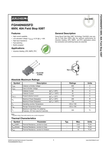
FGH40N60SFD 600V, 40A Field Stop IGBT
FGH40N60SFD 600V, 40A Field Stop IGBT
FGH40N60SFD 600V, 40A Field Stop IGBT

You also want an ePaper? Increase the reach of your titles
YUMPU automatically turns print PDFs into web optimized ePapers that Google loves.
<strong>FGH40N60SFD</strong><br />
<strong>600V</strong>, <strong>40A</strong> <strong>Field</strong> <strong>Stop</strong> <strong>IGBT</strong><br />
Features<br />
• High current capability<br />
• Low saturation voltage: V CE(sat) =2.3V @ I C = <strong>40A</strong><br />
• High input impedance<br />
• Fast switching<br />
• RoHS compliant<br />
Applications<br />
• Induction Heating, UPS, SMPS, PFC<br />
General Description<br />
July 2008<br />
tm<br />
Using Novel <strong>Field</strong> <strong>Stop</strong> <strong>IGBT</strong> Technology, Fairchild’s new sesries<br />
of <strong>Field</strong> <strong>Stop</strong> <strong>IGBT</strong>s offer the optimum performance for<br />
Induction Heating, UPS, SMPS and PFC applications where<br />
low conduction and switching losses are essential.<br />
<strong>FGH40N60SFD</strong> <strong>600V</strong>, <strong>40A</strong> <strong>Field</strong> <strong>Stop</strong> <strong>IGBT</strong><br />
E<br />
C<br />
G<br />
C<br />
G<br />
COLLECTOR<br />
(FLANGE)<br />
E<br />
Absolute Maximum Ratings<br />
Symbol Description Ratings Units<br />
V CES Collector to Emitter Voltage 600 V<br />
V GES Gate to Emitter Voltage ± 20 V<br />
I C<br />
Collector Current @ T C = 25 o C 80 A<br />
Collector Current @ T C = 100 o C 40 A<br />
I CM (1) Pulsed Collector Current @ T C = 25 o C 120 A<br />
P D<br />
Maximum Power Dissipation @ T C = 25 o C 290 W<br />
Maximum Power Dissipation @ T C = 100 o C 116 W<br />
T J Operating Junction Temperature -55 to +150 o C<br />
T stg Storage Temperature Range -55 to +150<br />
o C<br />
T L<br />
Maximum Lead Temp. for soldering<br />
Purposes, 1/8” from case for 5 seconds<br />
300 o C<br />
Notes:<br />
1: Repetitive rating: Pulse width limited by max. junction temperature<br />
Thermal Characteristics<br />
Symbol Parameter Typ. Max. Units<br />
R θJC (<strong>IGBT</strong>) Thermal Resistance, Junction to Case - 0.43 o C/W<br />
R θJC (Diode) Thermal Resistance, Junction to Case - 1.45<br />
o C/W<br />
R θJA Thermal Resistance, Junction to Ambient - 40 o C/W<br />
©2008 Fairchild Semiconductor Corporation 1 www.fairchildsemi.com<br />
<strong>FGH40N60SFD</strong> Rev.C
Package Marking and Ordering Information<br />
Packaging<br />
Max Qty<br />
Device Marking Device Package Type Qty per Tube per Box<br />
<strong>FGH40N60SFD</strong> <strong>FGH40N60SFD</strong>TU TO-247 Tube 30ea -<br />
Electrical Characteristics of the <strong>IGBT</strong> T C = 25°C unless otherwise noted<br />
Symbol Parameter Test Conditions Min. Typ. Max. Units<br />
Off Characteristics<br />
BV CES Collector to Emitter Breakdown Voltage V GE = 0V, I C = 250µA 600 - - V<br />
∆BV CES<br />
∆T J<br />
Temperature Coefficient of Breakdown<br />
Voltage<br />
V GE = 0V, I C = 250µA - 0.6 - V/ o C<br />
I CES Collector Cut-Off Current V CE = V CES , V GE = 0V - - 250 µA<br />
I GES G-E Leakage Current V GE = V GES , V CE = 0V - - ±400 nA<br />
On Characteristics<br />
V GE(th) G-E Threshold Voltage I C = 250µA, V CE = V GE 4.0 5.0 6.5 V<br />
V CE(sat)<br />
Collector to Emitter Saturation Voltage<br />
I C = <strong>40A</strong>, V GE = 15V - 2.3 2.9 V<br />
I C = <strong>40A</strong>, V GE = 15V,<br />
T C = 125 o C<br />
- 2.5 - V<br />
<strong>FGH40N60SFD</strong> <strong>600V</strong>, <strong>40A</strong> <strong>Field</strong> <strong>Stop</strong> <strong>IGBT</strong><br />
Dynamic Characteristics<br />
C ies Input Capacitance<br />
- 2110 - pF<br />
C oes Output Capacitance<br />
V CE = 30V , V GE = 0V,<br />
f = 1MHz<br />
- 200 - pF<br />
C res Reverse Transfer Capacitance - 60 - pF<br />
Switching Characteristics<br />
t d(on) Turn-On Delay Time<br />
- 25 - ns<br />
t r Rise Time - 42 - ns<br />
t d(off) Turn-Off Delay Time V CC = 400V, I C = <strong>40A</strong>,<br />
- 115 - ns<br />
t f Fall Time R G = 10Ω, V GE = 15V,<br />
- 27 54 ns<br />
E on Turn-On Switching Loss<br />
Inductive Load, T C = 25 o C<br />
- 1.13 - mJ<br />
E off Turn-Off Switching Loss - 0.31 - mJ<br />
E ts Total Switching Loss - 1.44 - mJ<br />
t d(on) Turn-On Delay Time<br />
- 24 - ns<br />
t r Rise Time - 43 - ns<br />
t d(off) Turn-Off Delay Time V CC = 400V, I C = <strong>40A</strong>,<br />
- 120 - ns<br />
t f Fall Time R G = 10Ω, V GE = 15V,<br />
- 30 - ns<br />
E on Turn-On Switching Loss<br />
Inductive Load, T C = 125 o C<br />
- 1.14 - mJ<br />
E off Turn-Off Switching Loss - 0.48 - mJ<br />
E ts Total Switching Loss - 1.62 - mJ<br />
Q g Total Gate Charge<br />
- 120 - nC<br />
Q ge Gate to Emitter Charge<br />
V CE = 400V, I C = <strong>40A</strong>,<br />
V GE = 15V<br />
- 14 - nC<br />
Q gc Gate to Collector Charge - 58 - nC<br />
<strong>FGH40N60SFD</strong> Rev. C<br />
2 www.fairchildsemi.com
Electrical Characteristics of the Diode T C = 25°C unless otherwise noted<br />
Symbol Parameter Test Conditions Min. Typ. Max Units<br />
V FM Diode Forward Voltage I F = 20A<br />
T C = 25 o C - 1.95 2.6<br />
V<br />
T C = 125 o C - 1.85 -<br />
t rr Diode Reverse Recovery Time<br />
T C = 25 o C - 45 -<br />
ns<br />
I ES =20A, dI ES /dt = 200A/µs<br />
T C = 125 o C - 140 -<br />
Q rr Diode Reverse Recovery Charge<br />
T C = 25 o C - 75 -<br />
nC<br />
T C = 125 o C - 375 -<br />
<strong>FGH40N60SFD</strong> <strong>600V</strong>, <strong>40A</strong> <strong>Field</strong> <strong>Stop</strong> <strong>IGBT</strong><br />
<strong>FGH40N60SFD</strong> Rev.C<br />
3 www.fairchildsemi.com
Typical Performance Characteristics<br />
Figure 1. Typical Output Characteristics<br />
Collector Current, IC [A]<br />
120<br />
T C = 25 o C<br />
100<br />
20V<br />
15V<br />
80<br />
12V<br />
60<br />
40<br />
10V<br />
20<br />
V GE = 8V<br />
0<br />
0.0 1.5 3.0 4.5 6.0<br />
Collector-Emitter Voltage, V CE [V]<br />
Figure 2. Typical Output Characteristics<br />
Collector Current, IC [A]<br />
120<br />
100<br />
80<br />
60<br />
40<br />
20<br />
T C = 125 o C<br />
20V<br />
15V<br />
12V<br />
10V<br />
V GE = 8V<br />
0<br />
0.0 1.5 3.0 4.5 6.0<br />
Collector-Emitter Voltage, V CE [V]<br />
<strong>FGH40N60SFD</strong> <strong>600V</strong>, <strong>40A</strong> <strong>Field</strong> <strong>Stop</strong> <strong>IGBT</strong><br />
Figure 3. Typical Saturation Voltage<br />
Characteristics<br />
Collector Current, IC [A]<br />
80<br />
60<br />
40<br />
20<br />
Common Emitter<br />
V GE = 15V<br />
T C = 25 o C<br />
T C = 125 o C<br />
Collector Current, I C<br />
[A]<br />
Figure 4. Transfer Characteristics<br />
120<br />
80<br />
40<br />
Common Emitter<br />
V CE = 20V<br />
T C = 25 o C<br />
T C = 125 o C<br />
0<br />
0 1 2 3 4<br />
Collector-Emitter Voltage, V CE [V]<br />
0<br />
6 8 10 12 13<br />
Gate-Emitter Voltage,V GE [V]<br />
Figure 5. Saturation Voltage vs. Case<br />
Temperature at Variant Current Level<br />
Collector-Emitter Voltage, VCE [V]<br />
4.0<br />
3.5<br />
3.0<br />
2.5<br />
2.0<br />
1.5<br />
Common Emitter<br />
V GE = 15V<br />
80A<br />
<strong>40A</strong><br />
I C = 20A<br />
1.0<br />
25 50 75 100 125<br />
Collector-EmitterCase Temperature, T C [ o C]<br />
Collector-Emitter Voltage, VCE [V]<br />
Figure 6. Saturation Voltage vs. V GE<br />
20<br />
16<br />
12<br />
8<br />
4<br />
I C = 20A<br />
<strong>40A</strong><br />
Common Emitter<br />
T C = -40 o C<br />
80A<br />
0<br />
4 8 12 16 20<br />
Gate-Emitter Voltage, V GE [V]<br />
<strong>FGH40N60SFD</strong> Rev. C<br />
4 www.fairchildsemi.com
Typical Performance Characteristics<br />
Figure 7. Saturation Voltage vs. V GE<br />
Collector-Emitter Voltage, VCE [V]<br />
20<br />
16<br />
12<br />
8<br />
4<br />
<strong>40A</strong><br />
I C = 20A<br />
80A<br />
Common Emitter<br />
T C = 25 o C<br />
0<br />
4 8 12 16 20<br />
Gate-Emitter Voltage, V GE [V]<br />
Figure 9. Capacitance Characteristics<br />
Capacitance [pF]<br />
5000<br />
4000<br />
3000<br />
2000<br />
1000<br />
C iss<br />
C oss<br />
C rss<br />
Common Emitter<br />
V GE = 0V, f = 1MHz<br />
T C = 25 o C<br />
Collector-Emitter Voltage, VCE [V]<br />
Figure 8. Saturation Voltage vs. V GE<br />
20<br />
16<br />
12<br />
8<br />
4<br />
<strong>40A</strong><br />
I C = 20A<br />
80A<br />
Common Emitter<br />
T C = 125 o C<br />
0<br />
4 8 12 16 20<br />
Gate-Emitter Voltage, V GE [V]<br />
Figure 10. Gate charge Characteristics<br />
Gate-Emitter Voltage, VGE [V]<br />
15<br />
12<br />
9<br />
6<br />
3<br />
Common Emitter<br />
T C = 25 o C<br />
V cc = 100V<br />
300V<br />
200V<br />
<strong>FGH40N60SFD</strong> <strong>600V</strong>, <strong>40A</strong> <strong>Field</strong> <strong>Stop</strong> <strong>IGBT</strong><br />
0<br />
0.1 1 10<br />
Collector-Emitter Voltage, V CE [V]<br />
Figure 11. SOA Characteristics<br />
400<br />
0<br />
30 0 50 100 150<br />
Gate Charge, Q g [nC]<br />
Figure 12. Turn-on Characteristics vs.<br />
Gate Resistance<br />
200<br />
Collector Current, Ic [A]<br />
100<br />
10<br />
1<br />
0.1<br />
Single Nonrepetitive<br />
Pulse T C = 25 o C<br />
Curves must be derated<br />
linearly with increase<br />
in temperature<br />
10µs<br />
100µs<br />
1ms<br />
10 ms<br />
0.01<br />
1 10 100 1000<br />
Collector-Emitter Voltage, V CE [V]<br />
DC<br />
Switching Time [ns]<br />
100<br />
t r<br />
t d(on)<br />
Common Emitter<br />
V CC = 400V, V GE = 15V<br />
I C = <strong>40A</strong><br />
T C = 25 o C<br />
T C = 125 o C<br />
10<br />
0 10 20 30 40 50<br />
Gate Resistance, R G [Ω]<br />
<strong>FGH40N60SFD</strong> Rev. C<br />
5 www.fairchildsemi.com
Typical Performance Characteristics<br />
Figure 13. Turn-off Characteristics vs.<br />
Gate Resistance<br />
Switching Time [ns]<br />
5500<br />
1000<br />
100<br />
Common Emitter<br />
V CC = 400V, V GE = 15V<br />
I C = <strong>40A</strong><br />
T C = 25 o C<br />
T C = 125 o C<br />
t d(off)<br />
10<br />
0 10 20 30 40 50<br />
Gate Resistance, R G [Ω]<br />
t f<br />
Switching Time [ns]<br />
Figure 14. Turn-on Characteristics vs.<br />
Collector Current<br />
500<br />
100<br />
Common Emitter<br />
V GE = 15V, R G = 10Ω<br />
T C = 25 o C<br />
T C = 125 o C<br />
10<br />
20 40 60 80<br />
Collector Current, I C [A]<br />
t r<br />
t d(on)<br />
<strong>FGH40N60SFD</strong> <strong>600V</strong>, <strong>40A</strong> <strong>Field</strong> <strong>Stop</strong> <strong>IGBT</strong><br />
Figure 15. Turn-off Characteristics vs.<br />
Collector Current<br />
Switching Time [ns]<br />
500<br />
100<br />
Common Emitter<br />
V GE = 15V, R G = 10Ω<br />
T C<br />
= 25 o C<br />
T C<br />
= 125 o C<br />
t d(off)<br />
t f<br />
Figure 16. Switching Loss vs. Gate Resistance<br />
Switching Loss [mJ]<br />
10<br />
1<br />
Common Emitter<br />
V CC = 400V, V GE = 15V<br />
I C = <strong>40A</strong><br />
T C<br />
= 25 o C<br />
T C = 125 o C<br />
E on<br />
E off<br />
10<br />
20 40 60 80<br />
Collector Current, I C [A]<br />
Figure 17. Switching Loss vs. Collector Current<br />
Switching Loss [mJ]<br />
30<br />
10<br />
1<br />
0.1<br />
Common Emitter<br />
V GE<br />
= 15V, R G<br />
= 10Ω<br />
T C<br />
= 25 o C<br />
T C = 125 o C<br />
20 30 40 50 60 70 80<br />
Collector Current, I C [A]<br />
E on<br />
E off<br />
0.3 0.2<br />
0 10 20 30 40 50<br />
Gate Resistance, R G [Ω]<br />
Figure 18. Turn off Switching<br />
SOA Characteristics<br />
Collector Current, IC [A]<br />
200<br />
100<br />
10<br />
Safe Operating Area<br />
V GE = 15V, T C = 125 o C<br />
1<br />
1 10 100 1000<br />
Collector-Emitter Voltage, V CE [V]<br />
<strong>FGH40N60SFD</strong> Rev. C<br />
6 www.fairchildsemi.com
Typical Performance Characteristics<br />
Figure 19. Forward Characteristics<br />
Forward Current, IF [A]<br />
80<br />
T J = 125 o C<br />
10<br />
T J = 25 o C<br />
T J = 75 o C<br />
1<br />
T C = 25 o C<br />
T C = 75 o C<br />
T C = 125 o C<br />
0.2<br />
0 1 2 3 4<br />
Forward Voltage, V F [V]<br />
Reverse Current , I R<br />
[µA]<br />
Figure 20. Typical Reverse Current vs.<br />
Reverse Voltage<br />
200<br />
100<br />
10<br />
1<br />
0.1<br />
T J = 125 o C<br />
T J = 75 o C<br />
T J = 25 o C<br />
0.01<br />
50 200 400 600<br />
Reverse Voltage, V R<br />
[V]<br />
<strong>FGH40N60SFD</strong> <strong>600V</strong>, <strong>40A</strong> <strong>Field</strong> <strong>Stop</strong> <strong>IGBT</strong><br />
Figure 21. Stored Charge<br />
100<br />
Figure 22. Reverse Recovery Time<br />
60<br />
Stored Recovery Charge, Qrr [nC]<br />
80<br />
60<br />
40<br />
200A/µs<br />
di/dt = 100A/µs<br />
Reverse Recovery Time, trr [ns]<br />
50<br />
40<br />
di/dt = 100A/µs<br />
200A/µs<br />
20<br />
5 10 20 30 40<br />
Forward Current, I F [A]<br />
30<br />
5 10 20 30 40<br />
Forward Current, I F [A]<br />
Figure 23.Transient Thermal Impedance of <strong>IGBT</strong><br />
1<br />
Thermal Response [Zthjc]<br />
0.1<br />
0.01<br />
0.5<br />
0.2<br />
0.1<br />
0.05<br />
0.02<br />
0.01<br />
single pulse<br />
Rectangular Pulse Duration [sec]<br />
P DM<br />
t 1<br />
t 2<br />
Duty Factor, D = t1/t2<br />
Peak T j = Pdm x Zthjc + T C<br />
1E-3<br />
1E-5 1E-4 1E-3 0.01 0.1 1<br />
<strong>FGH40N60SFD</strong> Rev. C<br />
7 www.fairchildsemi.com
Mechanical Dimensions<br />
TO-247AB (FKS PKG CODE 001)<br />
<strong>FGH40N60SFD</strong> <strong>600V</strong>, <strong>40A</strong> <strong>Field</strong> <strong>Stop</strong> <strong>IGBT</strong><br />
Dimensions in Millimeters<br />
<strong>FGH40N60SFD</strong> Rev. C<br />
8 www.fairchildsemi.com
tm<br />
tm<br />
tm<br />
TRADEMARKS<br />
The following includes registered and unregistered trademarks and service marks, owned by Fairchild Semiconductor and/or its global subsidianries, and is<br />
not intended to be an exhaustive list of all such trademarks.<br />
Build it Now<br />
CorePLUS<br />
CorePOWER<br />
CROSSVOLT<br />
CTL<br />
Current Transfer Logic<br />
EcoSPARK ®<br />
EfficentMax<br />
EZSWITCH *<br />
<br />
®<br />
Fairchild ®<br />
Fairchild Semiconductor ®<br />
FACT Quiet Series<br />
FACT ®<br />
FAST ®<br />
FastvCore<br />
FlashWriter ® *<br />
FPS<br />
F-PFS<br />
FRFET ®<br />
Global Power Resource SM<br />
Green FPS<br />
Green FPS e-Series<br />
GTO<br />
IntelliMAX<br />
ISOPLANAR<br />
MegaBuck<br />
MICROCOUPLER<br />
MicroFET<br />
MicroPak<br />
MillerDrive<br />
MotionMax<br />
Motion-SPM<br />
OPTOLOGIC ®<br />
OPTOPLANAR ®<br />
®<br />
PDP SPM<br />
Power-SPM<br />
PowerTrench ®<br />
Programmable Active Droop<br />
QFET ®<br />
QS<br />
Quiet Series<br />
RapidConfigure<br />
Saving our world, 1mW at a time<br />
SmartMax<br />
SMART START<br />
SPM ®<br />
STEALTH<br />
SuperFET<br />
SuperSOT-3<br />
SuperSOT-6<br />
SuperSOT-8<br />
SupreMOS<br />
SyncFET<br />
®<br />
* EZSWITCH and FlashWriter ® are trademarks of System General Corporation, used under license by Fairchild Semiconductor.<br />
The Power Franchise ®<br />
TinyBoost<br />
TinyBuck<br />
TinyLogic ®<br />
TINYOPTO<br />
TinyPower<br />
TinyPWM<br />
TinyWire<br />
UHC ®<br />
Ultra FRFET<br />
UniFET<br />
VCX<br />
VisualMax<br />
DISCLAIMER<br />
FAIRCHILD SEMICONDUCTOR RESERVES THE RIGHT TO MAKE CHANGES WITHOUT FURTHER NOTICE TO ANY PRODUCTS HEREIN TO IMPROVE<br />
RELIABILITY, FUNCTION, OR DESIGN. FAIRCHILD DOES NOT ASSUME ANY LIABILITY ARISING OUT OF THE APPLICATION OR USE OF ANY<br />
PRODUCT OR CIRCUIT DESCRIBED HEREIN; NEITHER DOES IT CONVEY ANY LICENSE UNDER ITS PATENT RIGHTS, NOR THE RIGHTS OF OTHERS.<br />
THESE SPECIFICATIONS DO NOT EXPAND THE TERMS OF FAIRCHILD’S WORLDWIDE TERMS AND CONDITIONS, SPECIFICALLY THE WARRANTY<br />
THEREIN, WHICH COVERS THESE PRODUCTS.<br />
LIFE SUPPORT POLICY<br />
FAIRCHILD’S PRODUCTS ARE NOT AUTHORIZED FOR USE AS CRITICAL COMPONENTS IN LIFE SUPPORT DEVICES OR SYSTEMS WITHOUT THE<br />
EXPRESS WRITTEN APPROVAL OF FAIRCHILD SEMICONDUCTOR CORPORATION.<br />
As used herein:<br />
1. Life support devices or systems are devices or systems which, (a) are<br />
intended for surgical implant into the body or (b) support or sustain life,<br />
and (c) whose failure to perform when properly used in accordance with<br />
instructions for use provided in the labeling, can be reasonably<br />
expected to result in a significant injury of the user.<br />
2. A critical component in any component of a life support, device, or<br />
system whose failure to perform can be reasonably expected to cause<br />
the failure of the life support device or system, or to affect its safety or<br />
effectiveness.<br />
ANTI-COUNTERFEITING POLICY<br />
Fairchild Semiconductor Corporation’s Anti-Counterfeiting Policy. Farichild’s Anti-Counterfeiting Policy is also stated on our external website,<br />
www.fairchildsemi.com, under Sales Support.<br />
Counterfeiting of semiconductor parts is a growing problem in the industry. All manufactures of semiconductor products are experiencing counterfeiting of their<br />
parts. Customers who inadvertently purchase counterfeit parts experience many problems such as loss of brand reputation, substandard performance, failed<br />
application, and increased cost of production and manufacturing delays. Fairchild is taking strong measures to protect ourselves and our customers from the<br />
proliferation of counterfeit parts. Farichild strongly encourages customers to purchase Farichild parts either directly from Fairchild or from Authorized Fairchild<br />
Distributors who are listed by country on our web page cited above. Products customers buy either from fairchild directly or from Authorized Fairchild<br />
Distributors are genuine parts, have full traceability, meet Fairchild’s quality standards for handing and storage and provide access to Farichild’s full range of<br />
up-to-date technical and product information. Fairchild and our Authorized Distributors will stand behind all warranties and will appropriately address and<br />
warranty issues that may arise. Fairchild will not provide any warranty coverage or other assistance for parts bought from Unauthorized Sources. Farichild is<br />
committed to committed to combat this global problem and encourage our customers to do their part in stopping this practice by buying direct or from authorized<br />
distributors.<br />
PRODUCT STATUS DEFINITIONS<br />
Definition of Terms<br />
Datasheet Identification Product Status Definition<br />
Advance Information<br />
Formative / In Design<br />
Datasheet contains the design specifications for product development. Specifications<br />
may change in any manner without notice.<br />
Preliminary<br />
No Identification Needed<br />
First Production<br />
Full Production<br />
Datasheet contains preliminary data; supplementary data will be published at a later<br />
date. Fairchild Semiconductor reserves the right to make changes at any time without<br />
notice to improve design.<br />
Datasheet contains final specifications. Fairchild Semiconductor reserves the right to<br />
make changes at any time without notice to improve the design.<br />
Obsolete<br />
Not In Production<br />
Datasheet contains specifications on a product that is discontinued by Fairchild<br />
Semiconductor. The datasheet is for reference information only.<br />
Rev. I35