Electrical Properties of Pulsed Laser Crystallized Silicon Films
Electrical Properties of Pulsed Laser Crystallized Silicon Films
Electrical Properties of Pulsed Laser Crystallized Silicon Films

You also want an ePaper? Increase the reach of your titles
YUMPU automatically turns print PDFs into web optimized ePapers that Google loves.
Jpn. J. Appl. Phys. Vol. 38 (1999) pp. 1892–1897<br />
Part 1, No. 4A, April 1999<br />
c○1999 Publication Board, Japanese Journal <strong>of</strong> Applied Physics<br />
<strong>Electrical</strong> <strong>Properties</strong> <strong>of</strong> <strong>Pulsed</strong> <strong>Laser</strong> <strong>Crystallized</strong> <strong>Silicon</strong> <strong>Films</strong><br />
Toshiyuki SAMESHIMA, Keiko SAITOH, Naho AOYAMA, Seiichiro HIGASHI 1 ,<br />
Michio KONDO 2 and Akihisa MATSUDA 2<br />
Tokyo University <strong>of</strong> Agriculture & Technology, Tokyo 184-8588, Japan<br />
1 SEIKO Epson Corporation, Nagano 392-8502, Japan<br />
2 Electrotechnical Laboratory, Ibaraki 305-8568, Japan<br />
(Received October 21, 1998; revised manuscript received December 16, 1998; accepted for publication December 28, 1998)<br />
<strong>Electrical</strong> properties <strong>of</strong> phosphorus-doped laser-crystallized silicon films were investigated. The analysis <strong>of</strong> free carrier<br />
optical absorption revealed that crystalline grains formed at laser energies <strong>of</strong> 360–375 mJ/cm 2 had high carrier mobilities <strong>of</strong><br />
40–50 cm 2 /Vs, which were close to that <strong>of</strong> doped single crystalline silicon. The mobility did not depend on the number <strong>of</strong><br />
laser pulses. On the other hand, Hall effect measurements showed a marked increase in the carrier mobility <strong>of</strong> electrical current<br />
traversing grain boundaries from 3 to 28 cm 2 /Vs as the laser energy density increased from 160 to 375 mJ/cm 2 . The Hall<br />
mobility also increased as the number <strong>of</strong> laser pulses increased, although a single pulse irradiation resulted in a maximum<br />
carrier mobility <strong>of</strong> 15 cm 2 /Vs. These results suggest that a high laser energy density as well as numbers <strong>of</strong> multiple pulses are<br />
necessary to reduce disordered amorphous states and improve grain boundary properties.<br />
KEYWORDS: optical absorption spectra, free carrier absorption, Hall effect, carrier density, carrier mobility, E 2 peak height<br />
1. Introduction<br />
Polycrystalline silicon films are important for a variety <strong>of</strong><br />
applications in many devices such as thin film transistors<br />
(TFTs) and thin film solar cells. 1–10) The electrical properties<br />
<strong>of</strong> polycrystalline silicon films have been analyzed using<br />
Hall effect measurements and transistor characteristics.<br />
These measurements give the carrier mobility and the density<br />
<strong>of</strong> the carriers which propagate across many grain boundaries<br />
in polycrystalline silicon (poly-Si) films. The average<br />
energy barrier height at grain boundaries has also been investigated<br />
by these methods. We recently reported the possibility<br />
<strong>of</strong> investigating electrical properties <strong>of</strong> polycrystalline silicon<br />
films using free carrier optical absorption analysis. 11, 12) Because<br />
free carrier optical absorption occurs via excitation induced<br />
by the electrical field <strong>of</strong> incident photons followed by<br />
energy relaxation in the crystalline grains, the analysis gives<br />
the carrier mobility and the carrier density in the crystalline<br />
grains. On the other hand, the Hall effect measurement provides<br />
the effective carrier mobility <strong>of</strong> the electrical current,<br />
which traverses many grain boundaries, so it strongly depends<br />
on grain boundary properties.<br />
In this paper we discuss electrical properties by analyses<br />
<strong>of</strong> the free carrier optical absorption and Hall effect measurements<br />
<strong>of</strong> pulsed laser crystallized doped silicon films.<br />
The pulsed laser crystallization method is convenient to form<br />
polycrystalline silicon films at a low processing temperature<br />
because <strong>of</strong> local and rapid heat treatment. 13, 14) The method is<br />
suitable for fabrication <strong>of</strong> TFTs and solar cells at a low temperature.<br />
Optimization <strong>of</strong> crystallization, however, has not<br />
been achieved. Through the analyses <strong>of</strong> samples fabricated<br />
under different laser-irradiation conditions, we report the relationships<br />
between irradiation conditions (laser energy density<br />
and pulse number) and electrical properties (carrier mobility<br />
and the carrier density). The free carrier optical absorption<br />
analysis shows that the doped crystalline grains can have a<br />
high average carrier mobility, which is close to that <strong>of</strong> single<br />
crystalline silicon under the same carrier density. The pulse<br />
number is important for reduction <strong>of</strong> the average energy barrier<br />
height at grain boundaries and to increase the Hall mobility.<br />
We also discuss the crystalline state <strong>of</strong> the polycrystalline<br />
silicon films by measurements <strong>of</strong> theE 2 peak which appears<br />
in ultraviolet reflectivity spectra.<br />
2. Experimental<br />
Doped polycrystalline silicon films 50 nm thick were fabricated<br />
by XeCl excimer laser heating <strong>of</strong> low-pressure chemical<br />
vapor deposited (LPCVD) amorphous silicon films on<br />
quartz glass substrates. Prior to laser crystallization, phosphorus<br />
atoms were uniformly doped into the films through<br />
SiO 2 films coated on the silicon films by ion implantation at<br />
a density <strong>of</strong> 2.5 × 10 15 cm −2 and an energy <strong>of</strong> 80 keV. About<br />
50% phosphorus atoms were doped into the silicon films. After<br />
removing the top SiO 2 films, the samples were placed in a<br />
vacuum chamber, which was evacuated by a turbo-molecular<br />
pump to a level <strong>of</strong> 1 × 10 −4 Pa for laser irradiation. Variation<br />
<strong>of</strong> laser energy density in the beam was reduced to less<br />
than 3% <strong>of</strong> the average laser energy density by beam homogenizing<br />
optics. <strong>Laser</strong> light was effectively absorbed 10 nm<br />
deep in the silicon surface because <strong>of</strong> the large optical absorption<br />
coefficient <strong>of</strong> Si, ∼10 6 cm −1 , at 308 nm, and the silicon<br />
surface was heated to high temperatures. Above a thresh-<br />
old energy for crystallization <strong>of</strong> 160 mJ/cm 2 , crystallization<br />
occurs by solidification <strong>of</strong> molten silicon induced by laser<br />
irradiation. The solidification (crystallization) velocity was<br />
about 1 m/s, which was experimentally determined from the<br />
changes in the electrical conductivity <strong>of</strong> silicon films during<br />
and after laser irradiation using transient conductance measurements<br />
because liquid silicon has a high electrical conductivity<br />
<strong>of</strong> ∼10 4 S/cm. 15–17) It has been known that dopant atoms<br />
do not segregate from solid to liquid silicon (the segregation<br />
coefficient ∼1) under rapid solidification conditions induced<br />
by pulsed laser irradiation. 18) We hypothesized that phosphorus<br />
atoms were distributed uniformly in crystalline grains and<br />
at grain boundaries.<br />
Three kinds <strong>of</strong> laser irradiation were conducted for sample<br />
fabrication. 1) Multiple-step-laser energy irradiation<br />
was carried out. <strong>Laser</strong> energy density was increased from<br />
160 mJ/cm 2 to 400 mJ/cm 2 in 20–40 mJ/cm 2 steps. A single<br />
pulse or five pulses were irradiated at each laser energy density<br />
step. 2) To investigate the dependence <strong>of</strong> electrical properties<br />
on the number <strong>of</strong> laser pulses, samples were irradiated<br />
1892
Jpn. J. Appl. Phys. Vol. 38 (1999) Pt. 1, No. 4A T. SAMESHIMA et al. 1893<br />
by a laser with pulse numbers from one to twenty at the final<br />
laser energy density step. Prior to the final laser energy<br />
density step, the laser energy density was increased stepwise<br />
with five laser pulse irradiations at each laser energy density<br />
step. 3) Samples were also fabricated by laser irradiation with<br />
a single pulse at different energies.<br />
The Hall effect measurements by the van der Pauw method<br />
were carried out at room temperature for silicon films with an<br />
area <strong>of</strong> 5 mm × 5 mm with Al electrodes formed at each corner<br />
to obtain the carrier mobility and the carrier density.The<br />
Hall mobility,µ H , is deduced from the relation<br />
µ H = R H σ = r H µ D (1)<br />
R =<br />
where R H is the Hall constant, σ is the electrical conductivity,<br />
r H is the Hall scattering factor and µ D is the drift mobility.<br />
Optical reflectivity was measured in the wave number<br />
range between 400 and 4000 cm −1 by conventional Fourier<br />
transform infrared spectrometry (FTIR) to analyze optical absorption<br />
<strong>of</strong> free carriers in the doped silicon films. The sample<br />
was irradiated by infrared light with an incidence angle<br />
<strong>of</strong> 10 ◦ , and reflection was detected at a resolution <strong>of</strong> 4 cm −1 .<br />
Reflectivity spectra were analyzed by the optical interference<br />
effect at air/Si/substrate. Reflectivity (R) at the surface <strong>of</strong> the<br />
air/Si/substrate is given by 19)<br />
∣<br />
∣(r 0 + r 1 exp (i4πñ f dK)) (1 + r 0 r 1 exp (i4πñ f dK)) −1∣ ∣ ∣<br />
2<br />
r 0 = (1 −ñ f )(1 +ñ f ) −1 , r 1 = (ñ f −ñ SiO2 )(ñ f +ñ SiO2 ) −1<br />
(2)<br />
ñ f = n f + ik f , ñ SiO2 = n SiO2 + ik SiO2<br />
where d is the film thickness, K is the wave number, ñ f and ñ SiO2 are the complex refractive index <strong>of</strong> Si films and SiO 2<br />
substrate, respectively, which consist <strong>of</strong> the real refractive indexes (n f and n SiO2 ) and the extinction coefficients (k f and k SiO2 ).<br />
Undoped crystalline silicon is transparent (k f = 0) in the infrared region. On the other hand, SiO 2 has substantial absorption<br />
for wave numbers lower than 2000 cm −1 so that the reflectivity includes the optical absorption effect <strong>of</strong> the quartz substrate. A<br />
small reflection at the rear surface (air/substrate) was also considered in the calculation <strong>of</strong> the reflectivity <strong>of</strong> the samples.<br />
The free carrier optical absorption causes changes in the refractive index as well as in the extinction coefficient, as shown by<br />
the following equations; 12, 20) [<br />
n f = √ 1 n 2 Si<br />
{(n − A + 2 Si − A 2 e 2 } 0.5<br />
] 0.5<br />
A)2 +<br />
2 4π 2 m 2 c 2 µ 2 K 2<br />
[<br />
k f = √ 1 A − n 2 Si<br />
{(n + 2 Si − A 2 e 2 } 0.5<br />
] 0.5<br />
(3)<br />
A)2 +<br />
2 4π 2 m 2 c 2 µ 2 K 2<br />
A = Nmµ 2 ɛ −1<br />
0 (1 + 4π 2 m 2 µ 2 c 2 e −2 K 2 ) −1<br />
where n Si is the refractive index <strong>of</strong> undoped crystalline silicon,<br />
c is the velocity <strong>of</strong> light in vacuum, e is the electrical<br />
charge, m is the effective mass <strong>of</strong> the carrier, whose dependence<br />
on the carrier density was determined by Miyao et<br />
al., 21) K is the wave number, µ is the carrier mobility, and<br />
N is the carrier density. The experimental spectra were compared<br />
to the spectra obtained by the interference calculation<br />
given by eq. (1) with the refractive index and the extinction<br />
coefficient <strong>of</strong> silicon given by eq. (2) by changing the values<br />
<strong>of</strong> the parameters <strong>of</strong> carrier mobility and carrier density until<br />
best coincidence <strong>of</strong> those spectra was obtained.<br />
Optical reflectivity spectra in the ultraviolet region were<br />
also measured at the top silicon surface and the bottom silicon/quartz<br />
glass interface <strong>of</strong> the samples. Crystalline silicon<br />
has a broad peak around 276 nm (E 2 peak) in optical reflectivity<br />
which is caused by a large transition rate at the X<br />
point in the Brillouin zone, 22) while amorphous silicon has<br />
no peak around 276 nm. Because the optical absorption coefficient<br />
is large at ∼10 6 cm −1 in the ultraviolet region, the<br />
crystalline state at the surface and Si/SiO 2 interface regions<br />
can be investigated with 10 nm depth resolution. The height<br />
<strong>of</strong> the E 2 peak normalized by the peak reflectivity (R/R)<br />
was obtained to estimate crystalline states at both surfaces <strong>of</strong><br />
the polycrystalline silicon films. The reflectivity spectra at<br />
the bottom interface are different from those at the top surface<br />
because the refractive index <strong>of</strong> SiO 2 is larger than that <strong>of</strong><br />
air (= 1). Prior to the determination <strong>of</strong> R/R at the bottom<br />
interface, the reflectivity spectra were, therefore, corrected by<br />
multiplying a correction factor 0.73, which was obtained by<br />
calculations <strong>of</strong> reflectivity for SiO 2 /Si interfaces with different<br />
refractive indexes and extinction coefficients from amorphous<br />
to single crystalline silicon to reduce the effect <strong>of</strong> substrate<br />
on the reflectivity.<br />
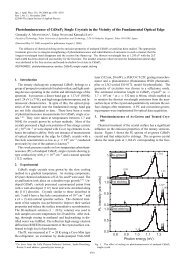
3. Results and Discussion<br />
Figure 1 shows experimental spectra for samples implanted<br />
with phosphorus atoms at a density <strong>of</strong> 2.5×10 15 cm −2 , which<br />
were fabricated by multiple-step laser energy irradiation with<br />
four final laser energies and five laser pulses at each laser energy<br />
density step. Although no crystallization <strong>of</strong> the silicon<br />
films and no activation <strong>of</strong> the phosphorus dopant atoms were<br />
observed in the lowest energy irradiation case, the crystallization<br />
and the reduction <strong>of</strong> electrical resistivity associated with<br />
dopant activation occurred in the other three cases <strong>of</strong> higher<br />
laser energy density. The reflectivity was reduced in the wave<br />
number range from 2000 to 4000 cm −1 as the laser energy<br />
density increased, as shown in Fig. 1. On the other hand, it<br />
increased in the wave number range from 500 to 800 cm −1 .<br />
These reflectivity changes resulted from changes in refractive<br />
index and extinction coefficient caused by free carrier optical<br />
absorption due to activation <strong>of</strong> the dopant atoms.<br />
Figure 2 shows the calculated reflectivity spectra <strong>of</strong> 50-
1894 Jpn. J. Appl. Phys. Vol. 38 (1999) Pt. 1, No. 4A T. SAMESHIMA et al.<br />
Reflectivity(%)<br />
70<br />
60<br />
40<br />
20<br />
0<br />
373<br />
286<br />
162<br />
111<br />
laser energy density(mJ/cm 2 )<br />
111<br />
162<br />
286<br />
373<br />
1000 2000 3000 4000<br />
Wave number(cm -1 )<br />
Fig. 1. Experimental reflectivity spectra for 50-nm-thick silicon films implanted<br />
with phosphorus atoms at a density <strong>of</strong> 2.5×10 15 cm −2 , which were<br />
fabricated by the multiple-step laser energy density irradiation method<br />
with four final laser energies and five laser pulses at each laser energy density<br />
step. The final laser energy is presented in the figure. The substrate<br />
was quartz glass.<br />
Reflectivity(%)<br />
Reflectivity(%)<br />
70<br />
60<br />
40<br />
20<br />
0<br />
70<br />
60<br />
40<br />
20<br />
0<br />
3.0<br />
2.5<br />
2.0<br />
1.5<br />
1.0<br />
carrier mobility : 40cm2/Vs<br />
carrier density(x1020cm -3 )<br />
0<br />
0.5<br />
1.0<br />
2.0 1.5<br />
2.5<br />
3.0<br />
0<br />
0.5<br />
1000 2000 3000 4000<br />
Wave number(cm -1 )<br />
(a)<br />
60<br />
20<br />
10<br />
5<br />
1 2<br />
carrier density : 2x1020cm -3<br />
carrier mobility(cm2/Vs)<br />
1<br />
2<br />
5<br />
10<br />
20<br />
60<br />
1000 2000 3000 4000<br />
Wave number(cm -1 )<br />
Fig. 2. Calculated reflectivity spectra <strong>of</strong> 50-nm-thick silicon/quartz substrates<br />
(a) with a carrier mobility <strong>of</strong> 40 cm 2 /Vs and different carrier densities<br />
from zero to 3 × 10 20 cm −3 , and (b) with a carrier density <strong>of</strong><br />
2×10 20 cm −3 and different carrier mobilities from 1 cm 2 /Vs to 60 cm 2 /Vs.<br />
nm-thick silicon/quartz substrates using eqs. (2) and (3) with<br />
a carrier mobility <strong>of</strong> 40 cm 2 /Vs and different carrier densities<br />
from zero to 3 × 10 20 cm −3 [Fig. 2(a)], and with a carrier<br />
density <strong>of</strong> 2 × 10 20 cm −3 and different carrier mobilities<br />
from 1 to 60 cm 2 /Vs [Fig. 2(b)]. The low carrier density and<br />
the low carrier mobility resulted in a monotonous increase<br />
in the reflectivity with increasing wave number from 1300 to<br />
4000 cm −1 and a low reflectivity at wave numbers between<br />
500 and 800 cm −1 . Reduction in the reflectivity was observed<br />
for wave numbers between 1300 and 4000 cm −1 as the carrier<br />
density and carrier mobility increased because the substantial<br />
free carrier optical absorption reduced the refractive<br />
index <strong>of</strong> silicon films (n f ). On the other hand, the reflectivity<br />
increased for wave numbers between 500 and 800 cm −1 as the<br />
(b)<br />
Carrier density(cm -3 )<br />
5x10²⁰<br />
4x10²⁰<br />
3x10²⁰<br />
2x10²⁰<br />
1x10²⁰<br />
Carrier mobility(cm 2 /Vs)<br />
free carrier absorption : 1pulse<br />
free carrier absorption : 5pulses<br />
Hall effect : 1pulse<br />
Hall effect : 5pulses<br />
0<br />
100 150 200 250 300 350 400<br />
<strong>Laser</strong> energy density(mJ/cm 2 )<br />
(a)<br />
50<br />
40<br />
30<br />
20<br />
10<br />
free carrier absorption : 5pulses<br />
free carrier absorption<br />
: 1pulse<br />
Hall effect : 5pulses<br />
Hall effect : 1pulse<br />
0<br />
100 150 200 250 300 350 400<br />
<strong>Laser</strong> energy density(mJ/cm 2 )<br />
(b)<br />
Fig. 3. (a) Carrier density and (b) carrier mobility obtained by analyses<br />
<strong>of</strong> free carrier optical absorption and by Hall effect measurements with<br />
the assumption <strong>of</strong> a Hall scattering factor <strong>of</strong> unity for phosphorus-doped<br />
50-nm-thick silicon films crystallized by laser irradiation, by increasing<br />
the laser energy density stepwise with one pulse and five pulses at each<br />
laser energy density step.<br />
carrier density and carrier mobility increased because the free<br />
carrier optical absorption causes an increase in the extinction<br />
coefficient <strong>of</strong> the silicon films (k f ) in that wave number range.<br />
Because the dependence <strong>of</strong> the refractive index or the extinction<br />
coefficient on the carrier density and the carrier mobility<br />
differs as shown in eq. (3), the calculation <strong>of</strong> reflectivity spectra<br />
most similar to experimental ones gives the carrier density<br />
and the carrier mobility.<br />
Figure 3 shows (a) the carrier density and (b) the carrier<br />
mobility obtained by analyses <strong>of</strong> free carrier optical absorption<br />
with best coincident fitting <strong>of</strong> calculated reflectivity spectra<br />
to experimental spectra for samples crystallized by laser irradiation<br />
by increasing the laser energy density stepwise one<br />
and five pulses at each laser energy density step. Figure 3<br />
also shows (a) the carrier density and (b) the carrier mobility<br />
obtained by Hall effect measurements when the Hall scattering<br />
factor was assumed to be equal to unity. Both analyses<br />
<strong>of</strong> free carrier optical absorption and Hall effect gave approximately<br />
the same carrier density, as shown in Fig. 3(a). The<br />
carrier density was slightly increased to 2.5×10 20 cm −3 as the<br />
laser energy density increased from 160 to 280 mJ/cm 2 , and it<br />
leveled <strong>of</strong>f at laser energy densities higher than 280 mJ/cm 2 .<br />
Dopant atoms were effectively activated and a high density<br />
<strong>of</strong> carriers was generated. An increase in carrier density with<br />
increasing laser energy density probably means that the activation<br />
was not completed over the entire film thickness in<br />
the low laser energy density region. The analysis <strong>of</strong> free<br />
carrier optical absorption gave a large carrier mobility about<br />
20 cm 2 /Vs at laser energy densities immediately above the<br />
crystallization threshold. The carrier mobility increased to<br />
40 cm 2 /Vs as the laser energy density increased. Irradiation<br />
with a single pulse and five pulses at each laser energy density<br />
step resulted in approximately the same carrier mobilities.
Jpn. J. Appl. Phys. Vol. 38 (1999) Pt. 1, No. 4A T. SAMESHIMA et al. 1895<br />
These results indicate that laser irradiation let to the formation<br />
<strong>of</strong> crystalline grains with good electrical characteristics<br />
even for lower laser energy densities near the crystallization<br />
threshold, although transmission electron microscopy (TEM)<br />
revealed that very fine crystalline grains with an average size<br />
<strong>of</strong> about 10 nm were formed by laser irradiation at the laser<br />
energy density <strong>of</strong> the crystallization threshold. 23) A gradual<br />
increase in the carrier mobility with increasing laser energy<br />
density probably resulted from the improvement <strong>of</strong> the crystalline<br />
properties; such as an increase in the average grain size<br />
or a reduction in the density <strong>of</strong> defect states. On the other<br />
hand, no change in the carrier mobility with number <strong>of</strong> laser<br />
pulses means that the number <strong>of</strong> laser pulses did not play an<br />
important role in the improvement <strong>of</strong> crystalline grain properties.<br />
The Hall effect measurements resulted in lower carrier<br />
mobilities than those obtained by the free carrier optical<br />
absorption analysis especially for samples treated with low<br />
laser energy densities. The carrier mobility obtained by the<br />
Hall effect measurements markedly increased as the laser energy<br />
density increased from 3 to 28 cm 2 /Vs. The degree <strong>of</strong><br />
increase in carrier mobility obtained by Hall effect measurements<br />
was much larger than that obtained by the free carrier<br />
optical absorption analysis. This large increase is interpreted<br />
as improvement in the grain boundary properties by laser irradiation<br />
with a high energy density, because the Hall mobility<br />
strongly depends on carrier trap states and a high potential<br />
energy barrier height at grain boundaries. Disordered states<br />
with a high density <strong>of</strong> dangling bonds at grain boundaries<br />
are reduced by high-energy irradiation because <strong>of</strong> the long<br />
melt duration and the low quenching rate. Moreover, the carrier<br />
mobility obtained by Hall effect measurements for samples<br />
crystallized with five pulses at each laser energy density<br />
step was higher than that for samples crystallized with single<br />
pulses at each laser energy density step for high final laser<br />
energy densities <strong>of</strong> 300–375 mJ/cm 2 .<br />
Figure 4 gives the carrier mobility as a function <strong>of</strong> the number<br />
<strong>of</strong> laser pulses from one to twenty at a final laser energy<br />
density <strong>of</strong> 360 mJ/cm 2 . Prior to the final laser energy density,<br />
five laser pulses were irradiated at each laser energy density<br />
step. Although the carrier mobility obtained by free carrier<br />
optical absorption analysis was 50 cm 2 /Vs, which did not<br />
depend on the number <strong>of</strong> laser pulses, the carrier mobility<br />
obtained by Hall effect measurements increased from 15 to<br />
25 mJ/cm 2 as the laser pulse number increased. This means<br />
that irradiation with multiple laser pulses is important to im-<br />
prove electrical properties at grain boundaries; the reformation<br />
<strong>of</strong> grain boundaries through melting followed by solidification<br />
might effectively reduce the density <strong>of</strong> carrier trap<br />
states and energy barrier heights. The maximum carrier mobility,<br />
∼50cm 2 /Vs, obtained by analysis <strong>of</strong> free carrier optical<br />
absorption was close to that <strong>of</strong> single crystalline doped silicon<br />
given by Irvin. 24) The crystalline grains have approximately<br />
the same electrical properties as doped single crystalline silicon.<br />
The crystalline state was investigated by measuring heights<br />
<strong>of</strong> the normalized E 2 peaks (R/R) at the top surface and<br />
the bottom interface for samples crystallized by laser irradiation<br />
by increasing the laser energy density stepwise with five<br />
pulses at each laser energy density step; the carrier density<br />
and carrier mobility are presented in Fig. 3. A smallE 2 peak<br />
was observed at both surfaces <strong>of</strong> silicon films for energies<br />
higher than the threshold energy. Low normalized E 2 peak<br />
height for irradiation at low laser energy density means that<br />
there are serious disordered amorphous states among the crystalline<br />
grains. The normalized E 2 peak heights (R/R) at<br />
both surfaces increased as the laser energy density increased.<br />
The crystallization occurred throughout the film thickness for<br />
energies immediately above the threshold energy density, and<br />
the crystalline volume fraction increased as the laser energy<br />
density increased. The normalized heights <strong>of</strong> the E 2 peak<br />
at the top surface were almost the same as the normalized<br />
height <strong>of</strong> the E 2 peak <strong>of</strong> single crystalline silicon for laser energy<br />
densities higher than 320 mJ/cm 2 . The crystalline state<br />
is dominant at the top surface region for those conditions <strong>of</strong><br />
high energy density.<br />
Changes in the heights <strong>of</strong> the E 2 peaks with the laser<br />
energy density correlated well with changes in the carrier<br />
mobility obtained by the analysis <strong>of</strong> free carrier optical absorption<br />
with the laser energy density, as shown in Figs. 3<br />
and 5. The improvement in crystalline state results in high<br />
carrier mobility. However, the normalized heights <strong>of</strong> the E 2<br />
peaks did not change substantially for laser energy densities<br />
above 320 mJ/cm 2 , while there was a marked increase<br />
in the Hall mobility with increasing laser energy densities<br />
above 320 mJ/cm 2 . Irradiation with high laser energy densities<br />
increased crystalline grain size and induced the formation<br />
<strong>of</strong> grain boundaries with almost zero thickness among crystalline<br />
grains with different orientation angles, as TEM observations<br />
suggested. 9, 10, 25) Moreover, irradiation with high<br />
laser energy densities and multiple pulses reduces the densi-<br />
Carrier mobility(cm 2 /Vs)<br />
70<br />
60<br />
50<br />
40<br />
30<br />
20<br />
laser energy density: 360 mJ/cm2<br />
free carrier absorption<br />
Hall effect<br />
10<br />
0 5 10 15 20 25<br />
<strong>Laser</strong> pulse number<br />
Fig. 4. Carrier mobilities obtained by analyses <strong>of</strong> free carrier absorption<br />
and by Hall effect measurements assuming a Hall scattering factor <strong>of</strong> unity<br />
as a function <strong>of</strong> number <strong>of</strong> pulses at a final energy density <strong>of</strong> 360 mJ/cm 2<br />
in the method <strong>of</strong> multiple-step laser energy density irradiation.<br />
Normalized E peak<br />
height (∆R/R)<br />
2<br />
0.20<br />
0.15<br />
0.10<br />
0.05<br />
single crystalline<br />
top surface<br />
bottom interface<br />
R<br />
r ∆R<br />
0<br />
λ<br />
100 150 200 250 300 350 400<br />
<strong>Laser</strong> energy density(mJ/cm 2 )<br />
Fig. 5. E 2 peak heights normalized by the peak reflectivity (R/R) at the<br />
top surface and the bottom interface for phosphorus-doped 50-nm-thick<br />
silicon films crystallized by laser irradiation by increasing the laser energy<br />
density stepwise with five pulses at each energy density step. The normalized<br />
E 2 peak height <strong>of</strong> single crystalline silicon, 0.172, is also shown.
1896 Jpn. J. Appl. Phys. Vol. 38 (1999) Pt. 1, No. 4A T. SAMESHIMA et al.<br />
ties <strong>of</strong> dangling bonds and weak bonds and reduces the average<br />
energy barrier heights via the formation <strong>of</strong> stable grain<br />
boundaries such as the coincident boundaries <strong>of</strong> the lattice<br />
sites that are electrically inactive, as suggested by various observations<br />
and theoretical calculations. 26–28) Defect states and<br />
potential energy barrier heights at grain boundaries can cause<br />
scattering <strong>of</strong> carriers and reduce the Hall scattering factor to<br />
be lower than unity. Although the Hall scattering factor was<br />
not determined in this study, Shirai and Serikawa reported<br />
a Hall scattering factor <strong>of</strong> 0.87 for laser crystallized silicon<br />
films, which was estimated experimentally from the Hall mobility<br />
and the field effect mobility <strong>of</strong> poly-Si TFTs. 29) Because<br />
similar field effect mobilities to that <strong>of</strong> Shirai and Serikawa’s<br />
TFTs was obtained for TFTs fabricated in poly-Si films by<br />
pulsed XeCl excimer laser irradiation with high laser energy<br />
densities near the amorphization threshold, 5) we deduce that<br />
the drift mobility was about 10% higher than the Hall mobility<br />
shown in Figs. 3 and 4 for cases <strong>of</strong> irradiation with high laser<br />
energy densities (> 300 mJ/cm 2 ). Because Le Bihan et al. reported<br />
a Hall scattering factor <strong>of</strong> 0.65 for solid phase crystallized<br />
silicon films with a higher density <strong>of</strong> trap states at grain<br />
boundaries than that <strong>of</strong> Shirai and Serikawa’s laser crystallized<br />
silicon films, 30) the Hall scattering factor might be lower<br />
than 0.87 for irradiation with lower laser energy densities near<br />
the crystallization threshold. According to this discussion, the<br />
average energy barrier height at grain boundaries (E) can be<br />
roughly estimated by assuming a simple relation between the<br />
drift mobility and the carrier mobility in crystalline grains,<br />
× µ H = µ A exp(−E/kT), where µ A , k and T<br />
are the average carrier mobility in crystalline grains obtained<br />
by the free carrier optical absorption, the Boltzmann constant<br />
and the absolute temperature, respectively. The minimum average<br />
energy barrier height was 11 meV under these laser irradiation<br />
conditions when the maximum average carrier mobility<br />
in crystalline grains, the maximum average Hall mobility<br />
and the Hall scattering factor were 50 cm 2 /Vs, 28 cm 2 /Vs and<br />
0.87, respectively.<br />
Figure 6 shows (a) the carrier density and (b) the carrier<br />
mobility for samples crystallized by laser irradiation with<br />
only one pulse. Both the analyses <strong>of</strong> free carrier optical absorption<br />
and Hall effect measurements assuming a Hall scattering<br />
factor <strong>of</strong> unity gave approximately the same carrier<br />
density, 1.7–2.5 × 10 20 cm −3 , for each laser energy density.<br />
The phosphorus atoms were effectively activated by a single<br />
laser pulse for laser energy densities from 165 to 400 mJ/cm 2 .<br />
The carrier mobility obtained by free carrier optical absorption<br />
analysis was larger than that obtained by Hall effect measurements.<br />
It had a maximum value <strong>of</strong> 38 cm 2 /Vs at laser energy<br />
densities <strong>of</strong> 260–80 mJ/cm 2 , which was approximately<br />
the same as the maximum mobility resulting from multiple-<br />
µ D = r −1<br />
H<br />
laser-pulse crystallization, as shown in Fig. 3. The highquality<br />
crystalline grains are formed by annealing with a single<br />
laser pulse. On the other hand, the maximum Hall mobility<br />
was 15 cm 2 /Vs, which was lower than the maximum<br />
carrier mobility for multiple-pulse irradiation. Single laser<br />
irradiation might not be sufficient to form a grain boundary<br />
with a low energy barrier. Carrier mobility decreased as the<br />
laser energy density increased from 280 to 400 mJ/cm 2 in<br />
contrast to the monotonous increase in the carrier mobility<br />
in the multiple-laser-pulse crystallization case, as shown in<br />
Figs. 3 and 6.<br />
Carrier density(cm-3)<br />
Normalized E peak<br />
height (∆R/R)<br />
2<br />
5x10 20<br />
4x10 20<br />
3x10 20<br />
2x10 20<br />
1x10 20<br />
Carrier mobility(cm 2 /Vs)<br />
0<br />
100 150 200 250 300 350 400<br />
<strong>Laser</strong> energy density(mJ/cm 2 )<br />
(a)<br />
50<br />
40<br />
30<br />
20<br />
10<br />
0.20<br />
0.15<br />
0.10<br />
0.05<br />
free carrier absorption<br />
Hall effect<br />
free carrier absorption<br />
Hall effect<br />
0<br />
100 150 200 250 300 350 400<br />
<strong>Laser</strong> energy density (mJ/cm 2 )<br />
Fig. 6. (a) Carrier density and (b) carrier mobility obtained by analyses <strong>of</strong><br />
free carrier optical absorption and by Hall effect measurements assuming<br />
a Hall scattering factor <strong>of</strong> unity for phosphorus-doped 50-nm-thick silicon<br />
films crystallized by laser irradiation with only one pulse.<br />
single crystalline<br />
top surface<br />
bottom interface<br />
0<br />
100 150 200 250 300 350 400<br />
<strong>Laser</strong> energy density(mJ/cm 2 )<br />
Fig. 7. E 2 peak heights normalized by the peak reflectivity (R/R) at the<br />
top surface and the bottom interface for phosphorus-doped 50-nm-thick<br />
silicon films crystallized by laser irradiation with only one pulse.<br />
The E 2 peak heights normalized by the peak reflectivity<br />
(R/R) at the top surface and the bottom interface were also<br />
measured for the single pulse crystallization case, and the results<br />
are shown in Fig. 7. The normalized E 2 peak heights<br />
at the both silicon surfaces increased as the laser energy density<br />
increased above the crystallization threshold, and reached<br />
a maximum at laser energy densities <strong>of</strong> 260–280 mJ/cm 2 ,<br />
which were coincident energy densities that gave a maximum<br />
value for carrier mobility, as shown in Fig. 6. The maximum<br />
value <strong>of</strong> the normalized peak heights (R/R) at both<br />
silicon surfaces was close to that <strong>of</strong> single crystalline silicon.<br />
The 50-nm-thick amorphous silicon films were crystallized<br />
entirely by a single laser pulse at laser energy densities<br />
<strong>of</strong> 260–280 mJ/cm 2 . The normalized heights <strong>of</strong> E 2<br />
peak at both silicon surfaces decreased as the laser energy<br />
density increased above 300 mJ/cm 2 . Disordered amorphous<br />
states are formed substantially above 300 mJ/cm 2 . The normalized<br />
heights <strong>of</strong> E 2 peak at the bottom interface decreased<br />
(b)
Jpn. J. Appl. Phys. Vol. 38 (1999) Pt. 1, No. 4A T. SAMESHIMA et al. 1897<br />
to smaller values than that at the top surface. The decrease<br />
in the carrier mobility and the normalized heights <strong>of</strong>E 2 peak<br />
with increasing laser energy density above 280 mJ/cm 2 shown<br />
in Figs. 6 and 7 was probably caused by microcrystallization,<br />
31) which occurs through rapid solidification <strong>of</strong> deepundercooled<br />
molten silicon induced by complete melting <strong>of</strong><br />
the silicon films. Very small ∼10 nm crystalline grains are<br />
formed through rapid crystallization, and disordered amorphous<br />
states are also formed. The microcrystalline state<br />
would dominate at the bottom interface because <strong>of</strong> small normalized<br />
E 2 peak heights at the bottom surface. Because<br />
amorphous silicon has a higher internal energy and a lower<br />
melting point than crystalline silicon, single pulse irradiation<br />
can melt a silicon film completely at lower laser energy densities<br />
compared with multiple-laser-pulse crystallization, which<br />
changes the films from amorphous to crystalline during the<br />
stepwise increase <strong>of</strong> laser energy density. Microcrystallization<br />
was not observed for laser energy densities lower than<br />
400 mJ/cm 2 in multiple-laser-pulse crystallization, as shown<br />
in Figs. 3 and 5.<br />
4. Summary<br />
The electrical properties <strong>of</strong> phosphorus-doped pulsed laser<br />
crystallized silicon films were investigated by analyses <strong>of</strong> free<br />
carrier optical absorption and Hall effect measurements. The<br />
analysis <strong>of</strong> free carrier optical absorption revealed that the<br />
carrier mobility increased from 20 to 40 cm 2 /Vs as the laser<br />
energy density increased from 160 to 375 mJ/cm 2 by XeCl excimer<br />
laser irradiation by increasing the laser energy density<br />
stepwise in vacuum for silicon films 50 nm thick implanted<br />
with phosphorus atoms at a density <strong>of</strong> 2.5 × 10 15 cm −2 . The<br />
mobility did not depend on number <strong>of</strong> laser pulses, and its<br />
maximum was close to that <strong>of</strong> doped single crystalline silicon.<br />
On the other hand, the carrier mobility obtained by Hall<br />
effect measurements markedly increased from 3 to 28 cm 2 /Vs<br />
as the laser energy density increased or the number <strong>of</strong> laser<br />
pulses increased. The E 2 peak height normalized by the peak<br />
reflectivity (R/R) at the top silicon surface and the bottom<br />
Si/substrate interface increased as the laser energy density<br />
increased. From these results, we interpret that crystalline<br />
grains formed by irradiation at laser energy densities above<br />
the crystallization threshold have good properties and high<br />
carrier mobility, but high laser energy densities as well as<br />
numbers <strong>of</strong> multiple pulses are required to reduce disordered<br />
amorphous states and improve grain boundary properties to<br />
increase the carrier mobility <strong>of</strong> electrical current traversing<br />
through grain boundaries. The energy barrier height was estimated<br />
to be 11 meV from the difference in the maximum<br />
mobilities obtained by these two methods. Single pulse irradiation<br />
caused crystallization <strong>of</strong> doped silicon films entirely,<br />
but the maximum carrier mobility was 15 cm 2 /Vs, which was<br />
lower than that obtained by multiple-pulse irradiation. In the<br />
case <strong>of</strong> single pulse irradiation, degradation <strong>of</strong> the crystalline<br />
state and reduction <strong>of</strong> carrier mobility probably caused by<br />
microcrystallization were observed for laser energy densities<br />
from 300–400 mJ/cm 2 , which were realized under cooling because<br />
<strong>of</strong> the low melting point <strong>of</strong> initial amorphous silicon.<br />
Acknowledgements<br />
The authors would like to thank H. Oshima, S.Inoue, T.<br />
Saitoh and T. Mohri for their support.<br />
1) T. Sameshima, S.Usui and M.Sekiya: IEEE Electron Device. Lett. 7<br />
(1986) 276.<br />
2) K. Sera, F. Okumura, H. Uchida, S, Itoh, S. Kaneko and K. Hotta: IEEE<br />
Trans. Electron Devices 36 (1989) 2868.<br />
3) T. Serikawa, S. Shirai, A. Okamoto and S.Suyama: Jpn. J. Appl. Phys.<br />
28 (1989) L1871.<br />
4) H. Kuriyama, T. Kuwahara, S. Ishida, T. Nohda, K. Sano, H. Iwata, S.<br />
Noguchi, S. Kiyama, S. Tsuda, S. Nakano, M. Osumi and Y. Kuwano:<br />
Jpn. J. Appl. Phys. 31 (1992) 4550.<br />
5) A. Kohno, T. Sameshima, N. Sano, M. Sekiya and M. Hara: IEEE Trans.<br />
Electron Devices 42 (1995) 251.<br />
6) M. Miyasaka, T. Komatsu, A. Shimodaira, I. Yudasaka and H. Ohshima:<br />
Jpn. J. Appl. Phys. 34 (1995) 921.<br />
7) A. Matsuda: J. Non-Cryst.Solids 56–60 (1983) 767.<br />
8) Y. Chida, M. Kondo and A. Matsuda: J. Non-Cryst. Solids 198–200<br />
(1996) 1121<br />
9) E. Fogarassy, B. Prevot, S. De Unamuno, E. Elliq, H. Pattyn, E. L. Mathe<br />
and A. Naudon: Appl. Phys. A 56 (1993) 365.<br />
10) P. Mei, J. B. Boyce, M. Hack, R. A. Lujan, R. I. Johnson, G. B. Anderson,<br />
D. K. Fork and S. E. Ready: Appl. Phys. Lett. 64 (1994) 1132.<br />
11) T. Sameshima, N. Takashima, K. Saitoh and N. Betsuda: Proc. Third<br />
Symp. Thin Film Transistor Technologies, ed. Y. Kuo (Electrochemical<br />
Society, Pennington, New Jersey, 1996) Vol. 96-23, p. 296<br />
12) T. Sameshima, K. Saitoh, M. Satoh, A. Tajima and N. Takashima: Jpn.<br />
J. Appl. Phys. 36 (1997) L1360.<br />
13) D. H. Lowndes, G. E. Jellison, Jr. and R. F. Wood: Phys. Rev. B 26<br />
(1982) 6747.<br />
14) T. Sameshima, M. Hara and S. Usui: Jpn. J. Appl. Phys. 28 (1989)<br />
L2131.<br />
15) G. J. Galvin, M. O. Thompson, J. W. Mayer, R. B. Hammond, N. Paulter<br />
and P. S. Peercy: Phys. Rev. Lett. 48 (1982) 33.<br />
16) V. M. Glazov, S. N. Chizhenvskaya and N. N. Glagoleva: Liquid Semiconductor<br />
(Plenum Press, New York, 1969) p. 60.<br />
17) T. Sameshima, M.Hara and S.Usui: Jpn. J. Appl. Phys. 28 (1989) 1789.<br />
18) R. F.Wood, J. R. Kirkpatrick and G. E. Giles: Phys. Rev. B 23 (1981)<br />
5555.<br />
19) M. Born and E.Wolf: Principles <strong>of</strong> Optics (Pergamon, New York, 1974)<br />
Chaps. 1 and 13.<br />
20) H. Engstrom; J. Appl. Phys. 51 (1980) 5245.<br />
21) M. Miyao, T. Motooda, N. Natuaki and T. Tokuyama: Proceeding in<br />
<strong>Laser</strong> and Electron-Beam Solid Interactions and Materials Processing<br />
(Elsevier, North Holland, Amsterdam, 1981) p. 163.<br />
22) J. R. Chelikowsky and M. L. Cohen: Phys. Rev. B 10 (1974) 5095.<br />
23) T. Sameshima and S. Usui: Mater. Res. Soc. Symp. Proc. 71 (1986) 435.<br />
24) J. C. Irvin: Bell Syst. Tech. J. 41 (1962) 387.<br />
25) J. S. Im, H. J. Kim and M. O. Thompson: Appl. Phys. Lett. 63 (1993)<br />
1969<br />
26) A. Bourret and J. J. Bacmann: Surf. Sci. 162 (1985) 495.<br />
27) A. T. Paxton and A. P. Sutton: J. Phys. C 21 (1988) L481.<br />
28) M. Koyama, R. Yamamoto R. Ebata and M. Kinoshita: J. Phys. C 21<br />
(1988) 3205.<br />
29) S. Shirai and T. Serikawa: IEEE Trans. Electron Devices 39 (1992) 450.<br />
30) F. Le Bihan, B. Fortin, H. Lhermite, O.Bonnaud and D. Briand: Polycrystalline<br />
Semiconductors III, eds H. P. Strunk, J. H. Werner, B. Fortin<br />
and O. Bonnaud (Scitec Publications, Zuerich-Uetikon, 1994) p. 379.<br />
31) T. Sameshima and S. Usui: Appl. Phys. Lett. 59 (1991) 2724.

![J. Magn. Magn. Mater.304 [1]](https://img.yumpu.com/36362486/1/184x260/j-magn-magn-mater304-1.jpg?quality=85)