Improvement of SiO2 Properties and Silicon Surface Passivation by ...
Improvement of SiO2 Properties and Silicon Surface Passivation by ...
Improvement of SiO2 Properties and Silicon Surface Passivation by ...

Create successful ePaper yourself
Turn your PDF publications into a flip-book with our unique Google optimized e-Paper software.
Jpn. J. Appl. Phys. Vol. 37 (1998) pp. L 1452–L 1454<br />
Part 2, No. 12A, 1 December 1998<br />
c○1998 Publication Board, Japanese Journal <strong>of</strong> Applied Physics<br />
<strong>Improvement</strong> <strong>of</strong> SiO 2 <strong>Properties</strong> <strong>and</strong> <strong>Silicon</strong> <strong>Surface</strong> <strong>Passivation</strong><br />
<strong>by</strong> Heat Treatment with High-Pressure H 2 O Vapor<br />
Toshiyuki SAMESHIMA, Keiji SAKAMOTO, Yoshiyuki TSUNODA <strong>and</strong> Tadashi SAITOH<br />
Tokyo University <strong>of</strong> Agriculture <strong>and</strong> Technology, 2-24-16 Nakamachi, Koganei, Tokyo 184-8588, Japan<br />
(Received August 28, 1998; accepted for publication October 7, 1998)<br />
Heat treatment with high-pressure H 2 O vapor was applied to improve the properties <strong>of</strong> SiO x (x < 2) films formed <strong>by</strong><br />
vacuum evaporation, for passivation <strong>of</strong> the silicon surface. Heat treatment at 340–420 ◦ C changed SiO x films into SiO 2 films<br />
with an Si–O–Si bonding network similar to that <strong>of</strong> thermally grown SiO 2 films. The densities <strong>of</strong> interface trap states <strong>and</strong> fixed<br />
positive charges were reduced to 6.5×10 10 cm −2 eV −1 <strong>and</strong> 2.5×10 11 cm −2 , respectively, after heat treatment at 340 ◦ C with<br />
2.4×10 6 -Pa–H 2 O vapor for 3 h. The heat treatment reduced the recombination velocity for the electron minority carriers from<br />
1200 cm/s (as fabricated) to 140 cm/s.<br />
KEYWORDS: SiO x , Si–O–Si bonding network, density <strong>of</strong> fixed positive charges, density <strong>of</strong> interface trap states, recombination<br />
velocity <strong>of</strong> minority carrier<br />
Although conventional solar cell passivation using thermal<br />
oxides requires temperatures between 850 ◦ C <strong>and</strong> 1050 ◦ C,<br />
many methods have been developed to establish low-cost,<br />
simple fabrication technologies. For example, plasmaenhanced<br />
chemical vapor deposition (PECVD) has become<br />
a promising technology for low temperature passivation <strong>of</strong><br />
solar cells. 1–3) Substrate temperatures during PECVD typically<br />
range between 250 ◦ C <strong>and</strong> 350 ◦ C. Recombination velocities<br />
lower than 100 cm/s have been reported for passivation<br />
using silicon oxide or silicon nitride films prepared<br />
<strong>by</strong> PECVD. Hydrogenation using hydrogen plasma or hydrogen<br />
radicals has also been widely investigated for the reduction<br />
<strong>of</strong> defects at the interface between insulator <strong>and</strong> silicon.<br />
4–6) We have reported simple heat treatment at approximately<br />
300 ◦ C with high-pressure H 2 O vapor, which improves<br />
the bulk properties <strong>of</strong> SiO 2 fabricated <strong>by</strong> PECVD,<br />
7, 8)<br />
as well as SiO 2 /single-crystalline Si interface properties.<br />
Heat treatment markedly reduces the density <strong>of</strong> the fixed oxide<br />
charges in SiO 2 films as well as the density <strong>of</strong> trap states<br />
<strong>of</strong> SiO 2 /Si, <strong>and</strong> reduces bonding strain at the SiO 2 /Si interfaces.<br />
In this paper, we propose a simple passivation method<br />
<strong>of</strong> the silicon surface using high-pressure H 2 O vapor annealing<br />
<strong>and</strong> SiO x -film evaporation. SiO x (x < 2) films are formed<br />
on silicon surfaces at room temperature <strong>by</strong> vacuum evaporation.<br />
9) Although they are defective, heat treatment with highpressure<br />
H 2 O vapor oxidizes SiO x films <strong>and</strong> improves the<br />
SiO x /Si interfaces. Increase in the minority carrier lifetime<br />
<strong>and</strong> decrease in the recombination velocity after the annealing<br />
are reported.<br />
SiO x films were formed on the silicon surface using a thermal<br />
evaporation method. A powder <strong>of</strong> SiO with a purity <strong>of</strong><br />
99.99 % was put in a Ta boat connected to electrodes placed<br />
in a vacuum chamber. A silicon substrate was placed above<br />
the boat. There was a shutter between the boat <strong>and</strong> the sample.<br />
The chamber was evacuated to a pressure <strong>of</strong> 3×10 −6 Torr.<br />
With the shutter closed, a voltage was applied to the Ta boat<br />
in order to heat it to just below the evaporation threshold for<br />
the desorption <strong>of</strong> gases adsorbed in the SiO powder, such as<br />
H 2 O as well as H 2 . After the pressure decreased to less than<br />
1×10 −5 Torr, the applied voltage was increased to realize a<br />
deposition rate <strong>of</strong> 40 nm/min. The shutter was then opened<br />
<strong>and</strong> the SiO evaporation initiated. The substrate temperature<br />
increased from room temperature to about 50 ◦ C owing to radiation<br />
emitted from the heated Ta boat.<br />
For heat treatment with high-pressure H 2 O vapor, samples<br />
were placed in a pressure-pro<strong>of</strong> stainless-steel chamber with<br />
a volume <strong>of</strong> 60 cm 3 using a metal seal. 7) Pure water was also<br />
put into the chamber. The samples were heated <strong>by</strong> placing<br />
the chamber on a heater plate. The H 2 O evaporated during<br />
heating <strong>and</strong> the gas pressure increased. Optical absorption<br />
spectra <strong>of</strong> SiO x films were measured using Fourier transform<br />
infrared spectrometry (FTIR) to investigate Si–O–Si bonding<br />
states. In order to investigate the electrical properties <strong>of</strong> the<br />
SiO 2 /Si interface, metal-oxide-semiconductor (MOS) capacitors<br />
were fabricated on p-type Si with an orientation <strong>of</strong> (100)<br />
<strong>and</strong> a resistivity <strong>of</strong> 10 cm −1 . Al was evaporated in vacuum<br />
<strong>and</strong> 100-nm-thick Al gate electrodes were formed at room<br />
temperature on the SiO x films just after deposition or after<br />
heat treatment with high-pressure H 2 O vapor. Capacitance<br />
responses at a frequency <strong>of</strong> 1 MHz were measured. The effective<br />
lifetime <strong>of</strong> excess minority carriers was also investigated<br />
for p-type Si with an orientation <strong>of</strong> (100) <strong>and</strong> a resistivity<br />
<strong>of</strong> 5000 cm, <strong>by</strong> measuring the decay in the reflectivity<br />
<strong>of</strong> a 14-GHz-microwave-probe when the excess minority carriers<br />
were induced <strong>by</strong> 200-ns-pulsed-laser irradiation with a<br />
wavelength <strong>of</strong> 940 nm, in order to estimate the recombination<br />
velocity at the silicon surface coated with 100-nm-thick SiO x<br />
10, 11)<br />
films.<br />
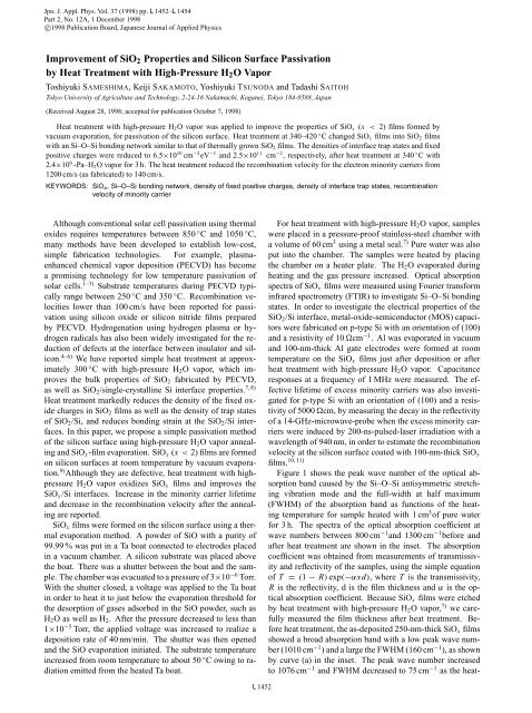
Figure 1 shows the peak wave number <strong>of</strong> the optical absorption<br />
b<strong>and</strong> caused <strong>by</strong> the Si–O–Si antisymmetric stretching<br />
vibration mode <strong>and</strong> the full-width at half maximum<br />
(FWHM) <strong>of</strong> the absorption b<strong>and</strong> as functions <strong>of</strong> the heating<br />
temperature for sample heated with 1 cm 3 <strong>of</strong> pure water<br />
for 3 h. The spectra <strong>of</strong> the optical absorption coefficient at<br />
wave numbers between 800 cm −1 <strong>and</strong> 1300 cm −1 before <strong>and</strong><br />
after heat treatment are shown in the inset. The absorption<br />
coefficient was obtained from measurements <strong>of</strong> transmissivity<br />
<strong>and</strong> reflectivity <strong>of</strong> the samples, using the simple equation<br />
<strong>of</strong> T = (1 − R) exp(−αxd), where T is the transmissivity,<br />
R is the reflectivity, d is the film thickness <strong>and</strong> α is the optical<br />
absorption coefficient. Because SiO x films were etched<br />
<strong>by</strong> heat treatment with high-pressure H 2 O vapor, 7) we carefully<br />
measured the film thickness after heat treatment. Before<br />
heat treatment, the as-deposited 250-nm-thick SiO x films<br />
showed a broad absorption b<strong>and</strong> with a low peak wave number<br />
(1010 cm −1 ) <strong>and</strong> a large the FWHM (160 cm −1 ), as shown<br />
<strong>by</strong> curve (a) in the inset. The peak wave number increased<br />
to 1076 cm −1 <strong>and</strong> FWHM decreased to 75 cm −1 as the heat-<br />
L 1452
Jpn. J. Appl. Phys. Vol. 37 (1998) Pt. 2, No. 12A T. SAMESHIMA et al. L 1453<br />
Fig. 1. The peak wave number <strong>of</strong> the optical absorption b<strong>and</strong> caused <strong>by</strong><br />
the Si–O–Si antisymmetric stretching vibration mode <strong>and</strong> its full-width at<br />
half maximum (FWHM) <strong>of</strong> the absorption b<strong>and</strong> as functions <strong>of</strong> the heating<br />
temperature when SiO x samples were heated with 1-cm 3 <strong>of</strong> pure water<br />
for 3 h. Inset shows optical absorption coefficient per unit film thickness<br />
for SiO x samples as-deposited (a) <strong>and</strong> annealed at 340 ◦ C (b). Dashed<br />
curve (c) is the spectrum <strong>of</strong> thermally grown SiO 2 at 1000 ◦ C, which was<br />
drawn with a maximum absorbance coincident with that <strong>of</strong> SiO x annealed<br />
at 340 ◦ C.<br />
Fig. 2. The total optical absorbance caused <strong>by</strong> the Si–O–Si antisymmetric<br />
stretching vibration mode per unit film thickness, which was obtained <strong>by</strong><br />
integration <strong>of</strong> the absorption coefficient from <strong>of</strong> 850 cm −1 to 1300 cm −1<br />
as a function <strong>of</strong> the reciprocal annealing temperature. Because 1 cm 3 <strong>of</strong><br />
pure water was used under every annealing condition, the H 2 O pressure<br />
was 1.4×10 6 Pa, 4.1×10 6 Pa, 4.7×10 6 Pa <strong>and</strong> 5.3×10 6 Pa for annealing<br />
temperatures <strong>of</strong> 180 ◦ C, 270 ◦ C, 340 ◦ C <strong>and</strong> 420 ◦ C, respectively. The total<br />
optical absorbances per unit film thickness <strong>of</strong> as-deposited SiO x <strong>and</strong><br />
thermally grown SiO 2 are also shown.<br />
1x10 13<br />
1x10 13<br />
1x10 12<br />
1x10 12<br />
1x10 11<br />
1x10 11<br />
1x10 10 1x10 10<br />
initial<br />
1.0 2.0 3.0 4.0 5.0<br />
Fig. 3. The densities <strong>of</strong> fixed positive charges <strong>and</strong> interface trap states<br />
as functions <strong>of</strong> H 2 O-vapor pressure. The SiO x samples were annealed<br />
at 340 ◦ C for 3 h. The experimental errors were 3×10 10 cm −2 <strong>and</strong><br />
5×10 10 cm −2 eV −1 for minimum densities <strong>of</strong> fixed positive charges <strong>and</strong><br />
interface trap states, respectively.<br />
ing temperature increased from 180 ◦ C to 420 ◦ C for highpressure<br />
H 2 O vapor annealing. The spectral line shape was<br />
markedly changed <strong>and</strong> became almost the same as that <strong>of</strong><br />
thermally grown SiO 2 films after heat treatment at temperatures<br />
<strong>of</strong> 340 ◦ C <strong>and</strong> 420 ◦ C, as shown <strong>by</strong> curves (b) <strong>and</strong> (c) in<br />
the inset. These optical changes mean that the annealed films<br />
had an Si–O–Si bonding network similar to that <strong>of</strong> thermally<br />
grown SiO 2 films. Figure 2 shows a total optical absorbance<br />
per unit film thickness, which was obtained <strong>by</strong> integration<br />
<strong>of</strong> the absorption coefficient from 850 cm −1 to 1300 cm −1 ,<br />
which corresponds to the volume density <strong>of</strong> Si–O bonds in<br />
the films, as a reciprocal function <strong>of</strong> annealing temperature.<br />
The initial SiO x films had a low total opticl absorbance per<br />
unit film thickness <strong>of</strong> 1.35×10 6 cm −2 , which is 0.49 times<br />
that <strong>of</strong> thermally grown SiO 2 films, because thermally evaporated<br />
SiO x films had many oxygen defects. The total optical<br />
absorbance per unit film thickness increased as the annealing<br />
temperature increased. The activation energy <strong>of</strong> increase<br />
in the total optical absorbance per unit film thickness<br />
was 0.064 eV, as shown in Fig. 2. This low activation energy<br />
means that the SiO x films can be easily oxidized <strong>by</strong> the heat<br />
treatment with high-pressure H 2 O vapor. The total optical<br />
absorbance per unit film thickness had a maximum value <strong>of</strong><br />
2.61×10 6 cm −2 when SiO x film was annealed at 340 ◦ C. It<br />
was 0.94 times that <strong>of</strong> thermally grown SiO 2 films. Because<br />
the absorption spectral line shape resulting from the Si–O–<br />
Si antisymmetric stretching vibration mode after annealing at<br />
340 ◦ C was almost the same as that <strong>of</strong> thermally grown SiO 2<br />
films, we hypothesize the existence <strong>of</strong> voids in the film, which<br />
reduce the average volume density <strong>of</strong> Si–O bonds. The thermal<br />
evaporation would not result in films as dense as thermally<br />
grown films. The total optical absorbance per unit film<br />
thickness for annealing at 420 ◦ C was lower than that for an-<br />
nealing at 340 ◦ C. Annealing at 420 ◦ C would cause substantial<br />
etching <strong>of</strong> Si–O bonds, especially weak bonds in the films,<br />
so that the density <strong>of</strong> voids would increase <strong>and</strong> the density <strong>of</strong><br />
Si–O bonds would decrease.<br />
Figure 3 shows the densities <strong>of</strong> interface trap states <strong>and</strong><br />
fixed positive charges as functions <strong>of</strong> H 2 O vapor pressure,<br />
obtained from the data <strong>of</strong> capacitance vs voltage applied to<br />
the MOS capacitors when the sample was annealed at 340 ◦ C<br />
for 3 h. The density <strong>of</strong> fixed positive charges was markedly<br />
reduced from 1.6×10 12 cm −2 to 5.6×10 10 cm −2 because the<br />
number <strong>of</strong> Si dangling bonds caused <strong>by</strong> oxygen defects was<br />
reduced through oxidization in high-pressure H 2 O vapor, so<br />
that the density <strong>of</strong> positive-charge-trapped states, for example
L 1454 Jpn. J. Appl. Phys. Vol. 37 (1998) Pt. 2, No. 12A T SAMESHIMA et al.<br />
.<br />
Fig. 4. The effective lifetime <strong>of</strong> electron excess minority carriers for p-type<br />
CZ silicon with a resistivity <strong>of</strong> 5000 cm, whose surfaces were coated<br />
with SiO x film, <strong>and</strong> the recombination velocity estimated from the effective<br />
lifetime as functions <strong>of</strong> H 2 O-vapor pressure. The samples were annealed<br />
at 340 ◦ C for 3 h. The experimental error <strong>of</strong> the maximum carrier<br />
lifetime was 50 µs so that the experimental error <strong>of</strong> the recombination<br />
velocity was 15 cm/s.<br />
the E’ center, was reduced. Although the density <strong>of</strong> interface<br />
trap states was high at 1.7×10 12 cm −2 eV −1 for as-deposited<br />
samples, it was reduced to 1.5×10 10 cm −2 eV −1 as H 2 O-vapor<br />
pressure was increased to 4.7×10 6 Pa. This result means that<br />
the Si dangling bonds at SiO 2 /Si interfaces were effectively<br />
reduced in number through low- temperature annealing with<br />
high-pressure H 2 O vapor. The effective lifetime <strong>of</strong> electronexcess<br />
minority carriers for p-type CZ silicon, whose surface<br />
was coated with SiO x films, was increased <strong>by</strong> heat treatment<br />
with high-pressure H 2 O vapor. The sample coated with asdeposited<br />
SiO x films had a low lifetime <strong>of</strong> 80 µs, as shown<br />
in Fig. 4, although it had a long lifetime <strong>of</strong> 2.8 ms when both<br />
bare surfaces were passivated with ethyl-alcohol liquid containing<br />
3 weight % iodine. 12) This means that there was a<br />
high density <strong>of</strong> trap states for electron minority carriers at<br />
the interfaces <strong>of</strong> as-deposited SiO x /Si. Heat treatment with<br />
high-pressure H 2 O vapor increased the lifetime <strong>of</strong> the minority<br />
carriers. The maximum lifetime was 580 µs, which<br />
was obtained after 2.4×10 6 Pa–H 2 O-vapor heat treatment, as<br />
shown in Fig. 4. The maximum lifetime gave the minimum<br />
carrier recombination velocity <strong>of</strong> 140 cm/s, although the recombination<br />
velocity was high, 1200 cm/s, for the case <strong>of</strong> asdeposited<br />
SiO x /Si, as shown in Fig. 4. An interesting result is<br />
that heat treatment with high-pressure H 2 O vapor reduced the<br />
carrier recombination velocity as well as the density <strong>of</strong> fixed<br />
positive charges. The field effect passivation caused <strong>by</strong> positive<br />
charges fixed in insulators is well known. 13) A high density<br />
<strong>of</strong> positive charges can cause an increase in the density<br />
<strong>of</strong> minority electron carriers at SiO 2 /Si interfaces <strong>and</strong> reduce<br />
their recombination velocity. The reduction in the density <strong>of</strong><br />
fixed positive charges means that the reduction in the recombination<br />
velocity results not from field effect passivation, but<br />
mainly from reduction in the density <strong>of</strong> the carrier trap states<br />
at the SiO 2 /Si interfaces.<br />
A simple method for passivation <strong>of</strong> the silicon surface was<br />
proposed. SiO x (x < 2) films were formed on silicon surfaces<br />
at room temperature <strong>by</strong> vacuum evaporation. Although<br />
they are defective <strong>and</strong> their Si–O bonding network was far<br />
different from that <strong>of</strong> thermally grown SiO 2 films, heat treatment<br />
with high-pressure H 2 O vapor oxidized SiO x films <strong>and</strong><br />
changed film properties so that they became similar to those<br />
<strong>of</strong> thermally grown SiO 2 films. The peak wave number <strong>of</strong> the<br />
optical absorption b<strong>and</strong> caused <strong>by</strong> the Si–O–Si antisymmetric<br />
stretching vibration mode was increased from 1010 cm −1<br />
(initial) to 1076 cm −1 after heat treatment at 420 ◦ C with<br />
4.7×10 6 Pa H 2 O vapor for 3 h, <strong>and</strong> the FWHM <strong>of</strong> the absorption<br />
b<strong>and</strong> was reduced from 160 cm −1 to 75 cm −1 . The<br />
volume density <strong>of</strong> Si–O bonds was increased with a thermal<br />
activation energy <strong>of</strong> 0.064 eV. The densities <strong>of</strong> interface<br />
trap states <strong>and</strong> fixed positive charges were reduced to<br />
6.5×10 10 cm −2 eV −1 <strong>and</strong> 2.5×10 11 cm −2 , respectively, after<br />
heat treatment at 340 ◦ C with 2.4×10 6 -Pa–H 2 O vapor for 3<br />
h. The effective lifetime <strong>of</strong> electron-excess minority carriers<br />
for p-type CZ silicon was increased from 80 µs to 580 µs after<br />
the heat treatment. This means that the recombination velocity<br />
was reduced from 1200 cm/s (as fabricated) to 140 cm/s.<br />
These results suggest that the present method will be useful<br />
for fabricating solar cells at a low temperature <strong>and</strong> at low cost.<br />
1) Z. Chen, S. K. Pang, K. Yasukake <strong>and</strong> A. Rohatigi: J. Appl. Phys. 74<br />
(1993) 2856.<br />
2) A. G. Aberle, T. Lauinger, J. Schmidt <strong>and</strong> R. Hezel: J. Appl. Phys. Lett.<br />
66 (1995) 2828.<br />
3) C. Leguijt, P. Loelgen, J. A. Eickelboom, A. S. H. van der Heide, R.<br />
A. Steeman, W. C. Sinke, P. M. Sarrp, L.A. Verhoef, P.-P. Michiels, Z.<br />
H. Chen <strong>and</strong> A. Rohatgi: Proc. in 12th Europ. Photovolt. Solar Energy<br />
Conf. (H. S. Stephens, Bedford, 1994) p. 720.<br />
4) S. J. Pertron, J. W. Corbett <strong>and</strong> T. S. Shi: Appl. Phys. A43 (1987) 153.<br />
5) H. Nagayoshi, Y. Onozawa, M. Ikeda, M. Yamaguchi, Y. Yamamoto,<br />
T. Uematsu, T.Saitoh <strong>and</strong> K. Kamisako: Jpn. J. Appl. Phys. 35 (1996)<br />
L1047.<br />
6) H. E. Elgamel, A. Rohatgi, Z. Chen, C. Vinckier, J. Nijs <strong>and</strong> R. Mertens:<br />
Proc. <strong>of</strong> 1st World Conference on Photovoltaic Energy Conversion,<br />
Hawaii, 1994 (IEEE, Salem) p. 1323.<br />
7) T. Sameshima <strong>and</strong> M. Satoh: Jpn. J. Appl. Phys. 36 (1997) L687.<br />
8) T. Sameshima, K. Sakamoto <strong>and</strong> M. Satoh: to be published in Thin<br />
Solid Films (1998).<br />
9) T. Sameshima, A. Kohno, M. Sekiya, M. Hara <strong>and</strong> N. Sano: Appl. Phys.<br />
Lett. 64 (1994) 1018.<br />
10) J. M. Borrego, R. J. Gutmann, N. Jensen <strong>and</strong> O. Paz: Solid-State Electron.<br />
30 (1987) 195.<br />
11) G. S. Kousik, Z. G. Ling <strong>and</strong> P. K. Ajmera: J. Appl. Phys. 72 (1992)<br />
141.<br />
12) T. S. Horanyi, T. Pavelka <strong>and</strong> P. Tuettoe: Appl. Surf. Sci. 63 (1993) 306.<br />
13) K. Yasutake, Z. Chen, S. K. Pang <strong>and</strong> A. Rohatgi: J. Appl. Phys. 75<br />
(1994) 2048.

![J. Magn. Magn. Mater.304 [1]](https://img.yumpu.com/36362486/1/184x260/j-magn-magn-mater304-1.jpg?quality=85)