Improvement of SiO2 Properties and Silicon Surface Passivation by ...
Improvement of SiO2 Properties and Silicon Surface Passivation by ...
Improvement of SiO2 Properties and Silicon Surface Passivation by ...

Create successful ePaper yourself
Turn your PDF publications into a flip-book with our unique Google optimized e-Paper software.
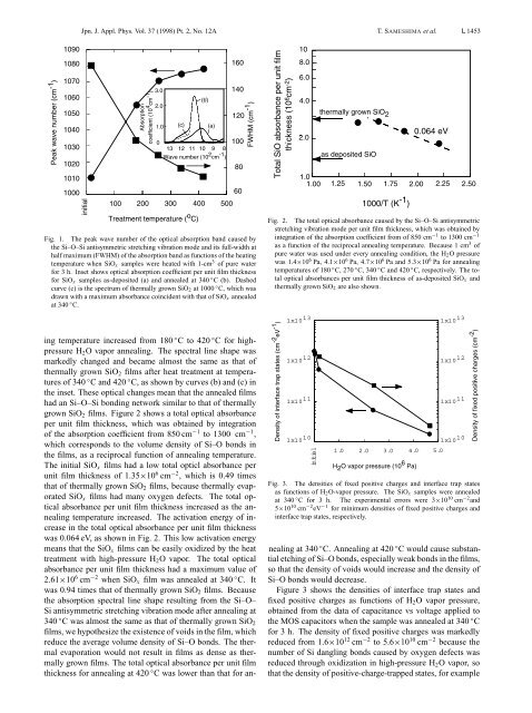
Jpn. J. Appl. Phys. Vol. 37 (1998) Pt. 2, No. 12A T. SAMESHIMA et al. L 1453<br />
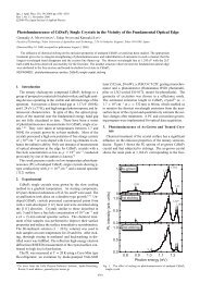
Fig. 1. The peak wave number <strong>of</strong> the optical absorption b<strong>and</strong> caused <strong>by</strong><br />
the Si–O–Si antisymmetric stretching vibration mode <strong>and</strong> its full-width at<br />
half maximum (FWHM) <strong>of</strong> the absorption b<strong>and</strong> as functions <strong>of</strong> the heating<br />
temperature when SiO x samples were heated with 1-cm 3 <strong>of</strong> pure water<br />
for 3 h. Inset shows optical absorption coefficient per unit film thickness<br />
for SiO x samples as-deposited (a) <strong>and</strong> annealed at 340 ◦ C (b). Dashed<br />
curve (c) is the spectrum <strong>of</strong> thermally grown SiO 2 at 1000 ◦ C, which was<br />
drawn with a maximum absorbance coincident with that <strong>of</strong> SiO x annealed<br />
at 340 ◦ C.<br />
Fig. 2. The total optical absorbance caused <strong>by</strong> the Si–O–Si antisymmetric<br />
stretching vibration mode per unit film thickness, which was obtained <strong>by</strong><br />
integration <strong>of</strong> the absorption coefficient from <strong>of</strong> 850 cm −1 to 1300 cm −1<br />
as a function <strong>of</strong> the reciprocal annealing temperature. Because 1 cm 3 <strong>of</strong><br />
pure water was used under every annealing condition, the H 2 O pressure<br />
was 1.4×10 6 Pa, 4.1×10 6 Pa, 4.7×10 6 Pa <strong>and</strong> 5.3×10 6 Pa for annealing<br />
temperatures <strong>of</strong> 180 ◦ C, 270 ◦ C, 340 ◦ C <strong>and</strong> 420 ◦ C, respectively. The total<br />
optical absorbances per unit film thickness <strong>of</strong> as-deposited SiO x <strong>and</strong><br />
thermally grown SiO 2 are also shown.<br />
1x10 13<br />
1x10 13<br />
1x10 12<br />
1x10 12<br />
1x10 11<br />
1x10 11<br />
1x10 10 1x10 10<br />
initial<br />
1.0 2.0 3.0 4.0 5.0<br />
Fig. 3. The densities <strong>of</strong> fixed positive charges <strong>and</strong> interface trap states<br />
as functions <strong>of</strong> H 2 O-vapor pressure. The SiO x samples were annealed<br />
at 340 ◦ C for 3 h. The experimental errors were 3×10 10 cm −2 <strong>and</strong><br />
5×10 10 cm −2 eV −1 for minimum densities <strong>of</strong> fixed positive charges <strong>and</strong><br />
interface trap states, respectively.<br />
ing temperature increased from 180 ◦ C to 420 ◦ C for highpressure<br />
H 2 O vapor annealing. The spectral line shape was<br />
markedly changed <strong>and</strong> became almost the same as that <strong>of</strong><br />
thermally grown SiO 2 films after heat treatment at temperatures<br />
<strong>of</strong> 340 ◦ C <strong>and</strong> 420 ◦ C, as shown <strong>by</strong> curves (b) <strong>and</strong> (c) in<br />
the inset. These optical changes mean that the annealed films<br />
had an Si–O–Si bonding network similar to that <strong>of</strong> thermally<br />
grown SiO 2 films. Figure 2 shows a total optical absorbance<br />
per unit film thickness, which was obtained <strong>by</strong> integration<br />
<strong>of</strong> the absorption coefficient from 850 cm −1 to 1300 cm −1 ,<br />
which corresponds to the volume density <strong>of</strong> Si–O bonds in<br />
the films, as a reciprocal function <strong>of</strong> annealing temperature.<br />
The initial SiO x films had a low total opticl absorbance per<br />
unit film thickness <strong>of</strong> 1.35×10 6 cm −2 , which is 0.49 times<br />
that <strong>of</strong> thermally grown SiO 2 films, because thermally evaporated<br />
SiO x films had many oxygen defects. The total optical<br />
absorbance per unit film thickness increased as the annealing<br />
temperature increased. The activation energy <strong>of</strong> increase<br />
in the total optical absorbance per unit film thickness<br />
was 0.064 eV, as shown in Fig. 2. This low activation energy<br />
means that the SiO x films can be easily oxidized <strong>by</strong> the heat<br />
treatment with high-pressure H 2 O vapor. The total optical<br />
absorbance per unit film thickness had a maximum value <strong>of</strong><br />
2.61×10 6 cm −2 when SiO x film was annealed at 340 ◦ C. It<br />
was 0.94 times that <strong>of</strong> thermally grown SiO 2 films. Because<br />
the absorption spectral line shape resulting from the Si–O–<br />
Si antisymmetric stretching vibration mode after annealing at<br />
340 ◦ C was almost the same as that <strong>of</strong> thermally grown SiO 2<br />
films, we hypothesize the existence <strong>of</strong> voids in the film, which<br />
reduce the average volume density <strong>of</strong> Si–O bonds. The thermal<br />
evaporation would not result in films as dense as thermally<br />
grown films. The total optical absorbance per unit film<br />
thickness for annealing at 420 ◦ C was lower than that for an-<br />
nealing at 340 ◦ C. Annealing at 420 ◦ C would cause substantial<br />
etching <strong>of</strong> Si–O bonds, especially weak bonds in the films,<br />
so that the density <strong>of</strong> voids would increase <strong>and</strong> the density <strong>of</strong><br />
Si–O bonds would decrease.<br />
Figure 3 shows the densities <strong>of</strong> interface trap states <strong>and</strong><br />
fixed positive charges as functions <strong>of</strong> H 2 O vapor pressure,<br />
obtained from the data <strong>of</strong> capacitance vs voltage applied to<br />
the MOS capacitors when the sample was annealed at 340 ◦ C<br />
for 3 h. The density <strong>of</strong> fixed positive charges was markedly<br />
reduced from 1.6×10 12 cm −2 to 5.6×10 10 cm −2 because the<br />
number <strong>of</strong> Si dangling bonds caused <strong>by</strong> oxygen defects was<br />
reduced through oxidization in high-pressure H 2 O vapor, so<br />
that the density <strong>of</strong> positive-charge-trapped states, for example

![J. Magn. Magn. Mater.304 [1]](https://img.yumpu.com/36362486/1/184x260/j-magn-magn-mater304-1.jpg?quality=85)