Device Simulation of Grain Boundaries in Lightly Doped Polysilicon ...
Device Simulation of Grain Boundaries in Lightly Doped Polysilicon ...
Device Simulation of Grain Boundaries in Lightly Doped Polysilicon ...

Create successful ePaper yourself
Turn your PDF publications into a flip-book with our unique Google optimized e-Paper software.
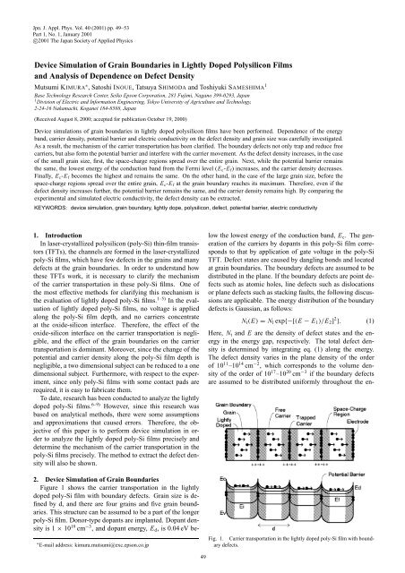
Jpn. J. Appl. Phys. Vol. 40 (2001) pp. 49–53Part 1, No. 1, January 2001c○2001 The Japan Society <strong>of</strong> Applied Physics<strong>Device</strong> <strong>Simulation</strong> <strong>of</strong> <strong>Gra<strong>in</strong></strong> <strong>Boundaries</strong> <strong>in</strong> <strong>Lightly</strong> <strong>Doped</strong> <strong>Polysilicon</strong> Filmsand Analysis <strong>of</strong> Dependence on Defect DensityMutsumi KIMURA ∗ , Satoshi INOUE, Tatsuya SHIMODA and Toshiyuki SAMESHIMA 1Base Technology Research Center, Seiko Epson Corporation, 281 Fujimi, Nagano 399-0293, Japan1 Division <strong>of</strong> Electric and Information Eng<strong>in</strong>eer<strong>in</strong>g, Tokyo University <strong>of</strong> Agriculture and Technology,2-24-16 Nakamachi, Koganei 184-8588, Japan(Received August 8, 2000; accepted for publication October 19, 2000)<strong>Device</strong> simulations <strong>of</strong> gra<strong>in</strong> boundaries <strong>in</strong> lightly doped polysilicon films have been performed. Dependence <strong>of</strong> the energyband, carrier density, potential barrier and electric conductivity on the defect density and gra<strong>in</strong> size was carefully <strong>in</strong>vestigated.As a result, the mechanism <strong>of</strong> the carrier transportation has been clarified. The boundary defects not only trap and reduce freecarriers, but also form the potential barrier and <strong>in</strong>terfere with the carrier movement. As the defect density <strong>in</strong>creases, <strong>in</strong> the case<strong>of</strong> the small gra<strong>in</strong> size, first, the space-charge regions spread over the entire gra<strong>in</strong>. Next, while the potential barrier rema<strong>in</strong>sthe same, the lowest energy <strong>of</strong> the conduction band from the Fermi level (E c -E f ) <strong>in</strong>creases, and the carrier density decreases.F<strong>in</strong>ally, E c -E f becomes the highest and rema<strong>in</strong>s the same. On the other hand, <strong>in</strong> the case <strong>of</strong> the large gra<strong>in</strong> size, before thespace-charge regions spread over the entire gra<strong>in</strong>, E c -E f at the gra<strong>in</strong> boundary reaches its maximum. Therefore, even if thedefect density <strong>in</strong>creases further, the potential barrier rema<strong>in</strong>s the same, and the carrier density rema<strong>in</strong>s high. By compar<strong>in</strong>g theexperimental and simulated electric conductivity, the defect density can be extracted.KEYWORDS: device simulation, gra<strong>in</strong> boundary, lightly dope, polysilicon, defect, potential barrier, electric conductivity1. IntroductionIn laser-crystallized polysilicon (poly-Si) th<strong>in</strong>-film transistors(TFTs), the channels are formed <strong>in</strong> the laser-crystallizedpoly-Si films, which have few defects <strong>in</strong> the gra<strong>in</strong>s and manydefects at the gra<strong>in</strong> boundaries. In order to understand howthese TFTs work, it is necessary to clarify the mechanism<strong>of</strong> the carrier transportation <strong>in</strong> these poly-Si films. One <strong>of</strong>the most effective methods for clarify<strong>in</strong>g this mechanism isthe evaluation <strong>of</strong> lightly doped poly-Si films. 1–5) In the evaluation<strong>of</strong> lightly doped poly-Si films, no voltage is appliedalong the poly-Si film depth, and no carriers concentrateat the oxide-silicon <strong>in</strong>terface. Therefore, the effect <strong>of</strong> theoxide-silicon <strong>in</strong>terface on the carrier transportation is negligible,and the effect <strong>of</strong> the gra<strong>in</strong> boundaries on the carriertransportation is dom<strong>in</strong>ant. Moreover, s<strong>in</strong>ce the change <strong>of</strong> thepotential and carrier density along the poly-Si film depth isnegligible, a two dimensional subject can be reduced to a onedimensional subject. Furthermore, with respect to the experiment,s<strong>in</strong>ce only poly-Si films with some contact pads arerequired, it is easy to fabricate them.To date, research has been conducted to analyze the lightlydoped poly-Si films. 6–9) However, s<strong>in</strong>ce this research wasbased on analytical methods, there were some assumptionsand approximations that caused errors. Therefore, the objective<strong>of</strong> this paper is to perform device simulation <strong>in</strong> orderto analyze the lightly doped poly-Si films precisely anddeterm<strong>in</strong>e the mechanism <strong>of</strong> the carrier transportation <strong>in</strong> thepoly-Si films precisely. The method to extract the defect densitywill also be shown.∗ E-mail address: kimura.mutsumi@exc.epson.co.jp2. <strong>Device</strong> <strong>Simulation</strong> <strong>of</strong> <strong>Gra<strong>in</strong></strong> <strong>Boundaries</strong>Figure 1 shows the carrier transportation <strong>in</strong> the lightlydoped poly-Si film with boundary defects. <strong>Gra<strong>in</strong></strong> size is def<strong>in</strong>edby d, and there are four gra<strong>in</strong>s and five gra<strong>in</strong> boundaries.This structure can be assumed to be a part <strong>of</strong> the longerpoly-Si film. Donor-type dopants are implanted. Dopant densityis 1 × 10 19 cm −3 , and dopant energy, E d , is 0.04 eV belowthe lowest energy <strong>of</strong> the conduction band, E c . The generation<strong>of</strong> the carriers by dopants <strong>in</strong> this poly-Si film correspondsto that by application <strong>of</strong> gate voltage <strong>in</strong> the poly-SiTFT. Defect states are caused by dangl<strong>in</strong>g bonds and locatedat gra<strong>in</strong> boundaries. The boundary defects are assumed to bedistributed <strong>in</strong> the plane. If the boundary defects are po<strong>in</strong>t defectssuch as atomic holes, l<strong>in</strong>e defects such as dislocationsor plane defects such as stack<strong>in</strong>g faults, the follow<strong>in</strong>g discussionsare applicable. The energy distribution <strong>of</strong> the boundarydefects is Gaussian, as follows:N t (E) = N l exp{−[(E − E 1 )/E 2 ] 2 }. (1)Here, N t and E are the density <strong>of</strong> defect states and the energy<strong>in</strong> the energy gap, respectively. The total defect densityis determ<strong>in</strong>ed by <strong>in</strong>tegrat<strong>in</strong>g eq. (1) along the energy.The defect density varies <strong>in</strong> the plane density <strong>of</strong> the order<strong>of</strong> 10 11 –10 14 cm −2 , which corresponds to the volume density<strong>of</strong> the order <strong>of</strong> 10 17 –10 20 cm −3 if the boundary defectsare assumed to be distributed uniformly throughout the en-Fig. 1. Carrier transportation <strong>in</strong> the lightly doped poly-Si film with boundarydefects.49
50 Jpn. J. Appl. Phys. Vol. 40 (2001) Pt. 1, No. 1 M. KIMURA et al.tire poly-Si film. For the as-crystallized poly-Si film, the defectdensity is very high. E 1 = 0 eV, which means that theboundary defects are distributed around the midgap <strong>in</strong> the energyband, and E 2 = 0.15 eV, which means that the Gaussianwidth is 0.3 eV. The boundary defects distributed around themidgap can be confirmed by the high potential barrier measured<strong>in</strong> an experiment. 5) The acceptor-like state is def<strong>in</strong>ed asa trap state that is neutral or negatively charged accord<strong>in</strong>g tothe Fermi level. The donor-like state is def<strong>in</strong>ed as a trap statethat is neutral or positively charged accord<strong>in</strong>g to the Fermilevel. It is assumed that the defect density <strong>of</strong> the acceptorlikestates and donor-like states are the same. This leads toa flat-band condition without the application <strong>of</strong> voltage. Thevoltage applied to both sides <strong>of</strong> the poly-Si film is 0.1 V.The donor-type dopants are ionized and generate free electroncarriers <strong>in</strong> the conduction band. The free carriers aretrapped at the boundary defects and decrease. On the otherhand, the boundary defects are charged negatively. In order topreserve charge neutrality, positive charges equal to negativecharges at the boundary defects are <strong>in</strong>duced on both sides <strong>of</strong>the gra<strong>in</strong> boundary. That is, the free carriers decreases on bothsides <strong>of</strong> the boundary, and space-charge regions are created bythe positive charges <strong>of</strong> the dopant ions. These space-chargeregions form a potential barrier at the boundary. The potentialbarrier <strong>in</strong>fluences the occupation probability <strong>of</strong> the boundarydefects, and the potential barrier and occupation probabilityare decided self-consistently. As a result, the boundarydefects <strong>in</strong>fluence the carrier transportation us<strong>in</strong>g two mechanisms.First, the boundary defects trap the free carriers andreduce them. Second, the boundary defects form the potentialbarrier and <strong>in</strong>terfere with the movement <strong>of</strong> the free carriers.Only the thermally activated free carriers can travel throughthe potential barrier.The device simulation can handle all the above-mentionedphenomena without any approximations. 10–12) In the devicesimulation, generally, the follow<strong>in</strong>g equations are utilized:ψ =−ρ/ε (2)∇·(−n n µ n E − D n ∇n n ) − G = 0 (3)∇·(n p µ p E − D p ∇n p ) − G = 0. (4)Equation (2) is the Poisson equation to calculate the potential.Equations (3) and (4) are the cont<strong>in</strong>uous equations for electronsand holes, respectively. These equations are based onthe drift-diffusion model and utilized to calculate the carriertransportation. The follow<strong>in</strong>g equations are also utilized:n n = N c exp[−(E c − E f )/(kT)] (5)n p = N v exp[−(E f − E v )/(kT)]. (6)Equations (5) and (6) are the carrier density equations forelectrons and holes, respectively. These equations are utilizedto relate the carrier density with the quasi Fermi level. Inthese equations, <strong>in</strong>stead <strong>of</strong> the Fermi-Dirac distribution, theMaxwell-Boltzmann distribution is utilized. Therefore, <strong>in</strong> thecase that the lowest energy <strong>of</strong> the conduction band or the highestenergy <strong>of</strong> the valence band is similar to the Fermi level,these equations are not valid. This occurs <strong>in</strong> the middle <strong>of</strong> thegra<strong>in</strong> for large gra<strong>in</strong> size and low defect density. However,s<strong>in</strong>ce the electric conductivity is high <strong>in</strong> this region, the effecton the total electric conductivity is not significant. Therefore,these equations can be utilized. In this paper, the follow<strong>in</strong>gequations are utilized:n d = N d (1/{1 + exp[(E f − E d )/(kT)]}) (7)∫n ta = N ta (E)(1/{1 + exp[(E − E f )/(kT)]})dE (8)∫n td = N td (E)(1/{1 + exp[(E f − E)/(kT)]})dE. (9)Equations (7), (8) and (9) are the occupation probability equationsfor donors, acceptor-like states and donor-like states, respectively.The follow<strong>in</strong>g equation is also utilized and substituted<strong>in</strong>to eq. (2):ρ = q(−n n + n p + n d − n ta + n td ). (10)In the device simulation, the structure is divided <strong>in</strong>to manymeshes, and eqs. (2)–(10) are formulated at each mesh. Byiterat<strong>in</strong>g to solve these equations and achiev<strong>in</strong>g convergence,the carrier density and potential can be calculated. F<strong>in</strong>ally, theenergy band, carrier density, potential barrier, electric conductivity,etc. can be calculated.3. Dependence on the Defect DensityDependence <strong>of</strong> the energy band, carrier density, potentialbarrier and electric conductivity on the defect density andFig. 2. Dependence <strong>of</strong> the (a) energy band and (b) carrier density with variations<strong>in</strong> the defect density for a gra<strong>in</strong> size <strong>of</strong> 10 nm.
Jpn. J. Appl. Phys. Vol. 40 (2001) Pt. 1, No. 1 M. KIMURA et al. 53portation has been clarified. The boundary defects not onlytrap and reduce free carriers, but also form the potential barrierand <strong>in</strong>terfere with the carrier movement. As the defectdensity <strong>in</strong>creases, <strong>in</strong> the case <strong>of</strong> the small gra<strong>in</strong> size, first,the space-charge regions spread over the entire gra<strong>in</strong>. Next,while the potential barrier rema<strong>in</strong>s the same, E c –E f <strong>in</strong>creases,and the carrier density decreases. F<strong>in</strong>ally, E c –E f becomes thehighest and rema<strong>in</strong>s the same. On the other hand, <strong>in</strong> the case<strong>of</strong> the large gra<strong>in</strong> size, before the space-charge regions spreadover the entire gra<strong>in</strong>, E c –E f at the gra<strong>in</strong> boundary reachesits maximum. Therefore, even if the defect density <strong>in</strong>creasesfurther, the potential barrier rema<strong>in</strong>s the same, and the carrierdensity rema<strong>in</strong>s high. By compar<strong>in</strong>g the experimentaland simulated electric conductivity, the defect density can beextracted.AcknowledgementsThe authors wish to thank Seiichiro Higashi <strong>of</strong> the SeikoEpson Corporation and Pr<strong>of</strong>essor Piero Migliorato <strong>of</strong> the University<strong>of</strong> Cambridge. The authors also wish to thank themembers <strong>of</strong> the Base Technology Research Center <strong>of</strong> theSeiko Epson Corporation, the Epson Cambridge Laboratory,Pr<strong>of</strong>essor Migliorato’s group at the University <strong>of</strong> Cambridgeand the LT Bus<strong>in</strong>ess Development Center <strong>of</strong> the Seiko EpsonCorporation.1) T. Sameshima, K. Saito, M. Sato, A. Tajima and N. Takashima: Jpn. J.Appl. Phys. 36 (1997) L1360.2) S. Higashi, K. Ozaki, K. Sakamoto, Y. Kano and T. Sameshima: Jpn. J.Appl. Phys. 38 (1999) L857.3) T. Sameshima, K. Saitoh, N. Aoyama, S. Higashi, M. Kondo and A.Matsuda: Jpn. J. Appl. Phys. 38 (1999) 1892.4) S. Higashi: Dig. AM-LCD ’99, Tokyo, 1999, p. 225.5) K. Sakamoto, Y. Tsunoda, T. Watanabe, K. Asada, T. Mohri, T.Sameshima and S. Higashi: Ext. Abstr. (60th Autumn Meet. 1999);The Japan Society <strong>of</strong> Applied Physics, Tokyo, p. 804 [<strong>in</strong> Japanese].6) J. Y. W. Seto: J. Appl. Phys. 46 (1975) 5247.7) G. Baccarani, B. Ricco and G. Spad<strong>in</strong>i: J. Appl. Phys. 49 (1978) 5565.8) P. V. Evans and S. F. Nelson: J. Appl. Phys. 69 (1991) 3605.9) T. Kam<strong>in</strong>s: Polycrystall<strong>in</strong>e Silicon for Integrated Circuits and Displays(Kluwer Academic Publishers, Boston, 1998) 2nd ed., Chap. 5, p. 199.10) S. Selberherr: Analysis and <strong>Simulation</strong> <strong>of</strong> Semiconductor <strong>Device</strong>s(Spr<strong>in</strong>ger-Verlag, Heidelberg, 1984).11) K. Taniguchi: Latest Semiconductor Process and <strong>Device</strong> <strong>Simulation</strong>Technology (Realize Inc., Tokyo, 1990).12) Silvaco International: <strong>Device</strong> Simulator Atlas.13) S. Higashi: private communication (2000).

![J. Magn. Magn. Mater.304 [1]](https://img.yumpu.com/36362486/1/184x260/j-magn-magn-mater304-1.jpg?quality=85)