Device Simulation of Grain Boundaries in Lightly Doped Polysilicon ...
Device Simulation of Grain Boundaries in Lightly Doped Polysilicon ...
Device Simulation of Grain Boundaries in Lightly Doped Polysilicon ...

Create successful ePaper yourself
Turn your PDF publications into a flip-book with our unique Google optimized e-Paper software.
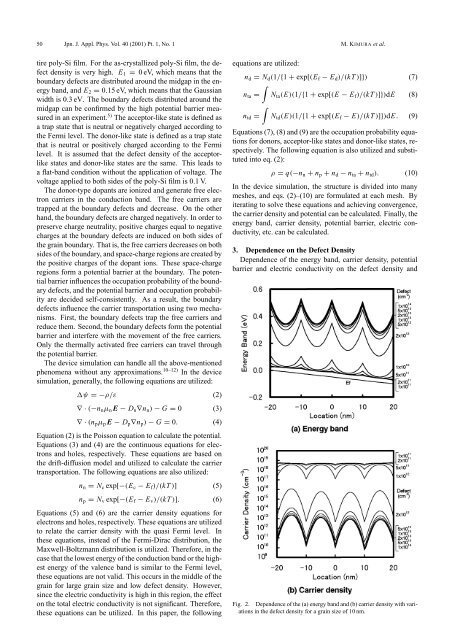
50 Jpn. J. Appl. Phys. Vol. 40 (2001) Pt. 1, No. 1 M. KIMURA et al.tire poly-Si film. For the as-crystallized poly-Si film, the defectdensity is very high. E 1 = 0 eV, which means that theboundary defects are distributed around the midgap <strong>in</strong> the energyband, and E 2 = 0.15 eV, which means that the Gaussianwidth is 0.3 eV. The boundary defects distributed around themidgap can be confirmed by the high potential barrier measured<strong>in</strong> an experiment. 5) The acceptor-like state is def<strong>in</strong>ed asa trap state that is neutral or negatively charged accord<strong>in</strong>g tothe Fermi level. The donor-like state is def<strong>in</strong>ed as a trap statethat is neutral or positively charged accord<strong>in</strong>g to the Fermilevel. It is assumed that the defect density <strong>of</strong> the acceptorlikestates and donor-like states are the same. This leads toa flat-band condition without the application <strong>of</strong> voltage. Thevoltage applied to both sides <strong>of</strong> the poly-Si film is 0.1 V.The donor-type dopants are ionized and generate free electroncarriers <strong>in</strong> the conduction band. The free carriers aretrapped at the boundary defects and decrease. On the otherhand, the boundary defects are charged negatively. In order topreserve charge neutrality, positive charges equal to negativecharges at the boundary defects are <strong>in</strong>duced on both sides <strong>of</strong>the gra<strong>in</strong> boundary. That is, the free carriers decreases on bothsides <strong>of</strong> the boundary, and space-charge regions are created bythe positive charges <strong>of</strong> the dopant ions. These space-chargeregions form a potential barrier at the boundary. The potentialbarrier <strong>in</strong>fluences the occupation probability <strong>of</strong> the boundarydefects, and the potential barrier and occupation probabilityare decided self-consistently. As a result, the boundarydefects <strong>in</strong>fluence the carrier transportation us<strong>in</strong>g two mechanisms.First, the boundary defects trap the free carriers andreduce them. Second, the boundary defects form the potentialbarrier and <strong>in</strong>terfere with the movement <strong>of</strong> the free carriers.Only the thermally activated free carriers can travel throughthe potential barrier.The device simulation can handle all the above-mentionedphenomena without any approximations. 10–12) In the devicesimulation, generally, the follow<strong>in</strong>g equations are utilized:ψ =−ρ/ε (2)∇·(−n n µ n E − D n ∇n n ) − G = 0 (3)∇·(n p µ p E − D p ∇n p ) − G = 0. (4)Equation (2) is the Poisson equation to calculate the potential.Equations (3) and (4) are the cont<strong>in</strong>uous equations for electronsand holes, respectively. These equations are based onthe drift-diffusion model and utilized to calculate the carriertransportation. The follow<strong>in</strong>g equations are also utilized:n n = N c exp[−(E c − E f )/(kT)] (5)n p = N v exp[−(E f − E v )/(kT)]. (6)Equations (5) and (6) are the carrier density equations forelectrons and holes, respectively. These equations are utilizedto relate the carrier density with the quasi Fermi level. Inthese equations, <strong>in</strong>stead <strong>of</strong> the Fermi-Dirac distribution, theMaxwell-Boltzmann distribution is utilized. Therefore, <strong>in</strong> thecase that the lowest energy <strong>of</strong> the conduction band or the highestenergy <strong>of</strong> the valence band is similar to the Fermi level,these equations are not valid. This occurs <strong>in</strong> the middle <strong>of</strong> thegra<strong>in</strong> for large gra<strong>in</strong> size and low defect density. However,s<strong>in</strong>ce the electric conductivity is high <strong>in</strong> this region, the effecton the total electric conductivity is not significant. Therefore,these equations can be utilized. In this paper, the follow<strong>in</strong>gequations are utilized:n d = N d (1/{1 + exp[(E f − E d )/(kT)]}) (7)∫n ta = N ta (E)(1/{1 + exp[(E − E f )/(kT)]})dE (8)∫n td = N td (E)(1/{1 + exp[(E f − E)/(kT)]})dE. (9)Equations (7), (8) and (9) are the occupation probability equationsfor donors, acceptor-like states and donor-like states, respectively.The follow<strong>in</strong>g equation is also utilized and substituted<strong>in</strong>to eq. (2):ρ = q(−n n + n p + n d − n ta + n td ). (10)In the device simulation, the structure is divided <strong>in</strong>to manymeshes, and eqs. (2)–(10) are formulated at each mesh. Byiterat<strong>in</strong>g to solve these equations and achiev<strong>in</strong>g convergence,the carrier density and potential can be calculated. F<strong>in</strong>ally, theenergy band, carrier density, potential barrier, electric conductivity,etc. can be calculated.3. Dependence on the Defect DensityDependence <strong>of</strong> the energy band, carrier density, potentialbarrier and electric conductivity on the defect density andFig. 2. Dependence <strong>of</strong> the (a) energy band and (b) carrier density with variations<strong>in</strong> the defect density for a gra<strong>in</strong> size <strong>of</strong> 10 nm.

![J. Magn. Magn. Mater.304 [1]](https://img.yumpu.com/36362486/1/184x260/j-magn-magn-mater304-1.jpg?quality=85)