Device Simulation of Grain Boundaries in Lightly Doped Polysilicon ...
Device Simulation of Grain Boundaries in Lightly Doped Polysilicon ...
Device Simulation of Grain Boundaries in Lightly Doped Polysilicon ...

You also want an ePaper? Increase the reach of your titles
YUMPU automatically turns print PDFs into web optimized ePapers that Google loves.
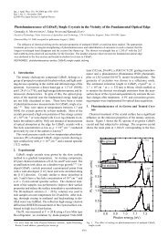
Jpn. J. Appl. Phys. Vol. 40 (2001) Pt. 1, No. 1 M. KIMURA et al. 53portation has been clarified. The boundary defects not onlytrap and reduce free carriers, but also form the potential barrierand <strong>in</strong>terfere with the carrier movement. As the defectdensity <strong>in</strong>creases, <strong>in</strong> the case <strong>of</strong> the small gra<strong>in</strong> size, first,the space-charge regions spread over the entire gra<strong>in</strong>. Next,while the potential barrier rema<strong>in</strong>s the same, E c –E f <strong>in</strong>creases,and the carrier density decreases. F<strong>in</strong>ally, E c –E f becomes thehighest and rema<strong>in</strong>s the same. On the other hand, <strong>in</strong> the case<strong>of</strong> the large gra<strong>in</strong> size, before the space-charge regions spreadover the entire gra<strong>in</strong>, E c –E f at the gra<strong>in</strong> boundary reachesits maximum. Therefore, even if the defect density <strong>in</strong>creasesfurther, the potential barrier rema<strong>in</strong>s the same, and the carrierdensity rema<strong>in</strong>s high. By compar<strong>in</strong>g the experimentaland simulated electric conductivity, the defect density can beextracted.AcknowledgementsThe authors wish to thank Seiichiro Higashi <strong>of</strong> the SeikoEpson Corporation and Pr<strong>of</strong>essor Piero Migliorato <strong>of</strong> the University<strong>of</strong> Cambridge. The authors also wish to thank themembers <strong>of</strong> the Base Technology Research Center <strong>of</strong> theSeiko Epson Corporation, the Epson Cambridge Laboratory,Pr<strong>of</strong>essor Migliorato’s group at the University <strong>of</strong> Cambridgeand the LT Bus<strong>in</strong>ess Development Center <strong>of</strong> the Seiko EpsonCorporation.1) T. Sameshima, K. Saito, M. Sato, A. Tajima and N. Takashima: Jpn. J.Appl. Phys. 36 (1997) L1360.2) S. Higashi, K. Ozaki, K. Sakamoto, Y. Kano and T. Sameshima: Jpn. J.Appl. Phys. 38 (1999) L857.3) T. Sameshima, K. Saitoh, N. Aoyama, S. Higashi, M. Kondo and A.Matsuda: Jpn. J. Appl. Phys. 38 (1999) 1892.4) S. Higashi: Dig. AM-LCD ’99, Tokyo, 1999, p. 225.5) K. Sakamoto, Y. Tsunoda, T. Watanabe, K. Asada, T. Mohri, T.Sameshima and S. Higashi: Ext. Abstr. (60th Autumn Meet. 1999);The Japan Society <strong>of</strong> Applied Physics, Tokyo, p. 804 [<strong>in</strong> Japanese].6) J. Y. W. Seto: J. Appl. Phys. 46 (1975) 5247.7) G. Baccarani, B. Ricco and G. Spad<strong>in</strong>i: J. Appl. Phys. 49 (1978) 5565.8) P. V. Evans and S. F. Nelson: J. Appl. Phys. 69 (1991) 3605.9) T. Kam<strong>in</strong>s: Polycrystall<strong>in</strong>e Silicon for Integrated Circuits and Displays(Kluwer Academic Publishers, Boston, 1998) 2nd ed., Chap. 5, p. 199.10) S. Selberherr: Analysis and <strong>Simulation</strong> <strong>of</strong> Semiconductor <strong>Device</strong>s(Spr<strong>in</strong>ger-Verlag, Heidelberg, 1984).11) K. Taniguchi: Latest Semiconductor Process and <strong>Device</strong> <strong>Simulation</strong>Technology (Realize Inc., Tokyo, 1990).12) Silvaco International: <strong>Device</strong> Simulator Atlas.13) S. Higashi: private communication (2000).

![J. Magn. Magn. Mater.304 [1]](https://img.yumpu.com/36362486/1/184x260/j-magn-magn-mater304-1.jpg?quality=85)