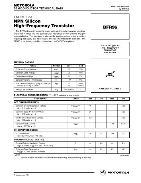
NPN Silicon High-Frequency Transistor BFR96
NPN Silicon High-Frequency Transistor BFR96
NPN Silicon High-Frequency Transistor BFR96

You also want an ePaper? Increase the reach of your titles
YUMPU automatically turns print PDFs into web optimized ePapers that Google loves.
SEMICONDUCTOR TECHNICAL DATA<br />
Order this document<br />
by <strong>BFR96</strong>/D<br />
The RF Line<br />
<br />
<br />
The <strong>BFR96</strong> transistor uses the same state–of–the–art microwave transistor<br />
chip which features fine–line geometry, ion–implanted arsenic emitters and gold<br />
top metallization. This transistor is intended for low–to–medium power amplifiers<br />
requiring high gain, low noise figure, and low intermodulation distortion. The<br />
<strong>BFR96</strong> is particularly suitable for broadband MATV/CATV amplifiers.<br />
<br />
fT = 4.5 GHz @ 50 mA<br />
HIGH–FREQUENCY<br />
TRANSISTOR<br />
<strong>NPN</strong> SILICON<br />
MAXIMUM RATINGS<br />
Rating Symbol Value Unit<br />
Collector–Emitter Voltage VCEO 15 Vdc<br />
Collector–Base Voltage VCBO 20 Vdc<br />
Emitter–Base Voltage VEBO 3.0 Vdc<br />
Collector Current — Continuous IC 100 mAdc<br />
Total Device Dissipation @ TC = 100°C (1)<br />
Derate above TC = 100°C<br />
PD 0.5<br />
10<br />
Watts<br />
mW/°C<br />
Storage Temperature Tstg –65 to +150 °C<br />
CASE 317A–01, STYLE 2<br />
ELECTRICAL CHARACTERISTICS (TC = 25°C unless otherwise noted.)<br />
OFF CHARACTERISTICS<br />
Collector–Emitter Breakdown Voltage<br />
(IC = 1.0 mAdc, IB = 0)<br />
Characteristic Symbol Min Typ Max Unit<br />
V(BR)CEO 15 — — Vdc<br />
Collector–Base Breakdown Voltage<br />
(IC = 100 µAdc, IE = 0)<br />
Emitter–Base Breakdown Voltage<br />
(IE = 100 µAdc, IC = 0)<br />
Collector Cutoff Current<br />
(VCB = 10 Vdc, IE = 0)<br />
ON CHARACTERISTICS<br />
DC Current Gain<br />
(IC = 50 mAdc, VCE = 10 Vdc)<br />
DYNAMIC CHARACTERISTICS<br />
Current–Gain — Bandwidth Product<br />
(IC = 50 mAdc, VCE = 10 Vdc, f = 0.5 GHz)<br />
Collector–Base Capacitance<br />
(VCB = 10 Vdc, Emitter Guarded)<br />
V(BR)CBO 20 — — Vdc<br />
V(BR)EBO 3.0 — — Vdc<br />
ICBO — — 100 nAdc<br />
hFE 30 — 200 —<br />
fT — 4.5 — GHz<br />
Ccb — 1.2 1.5 pF<br />
NOTE:<br />
1. Case temperature measured on collector lead immediately adjacent to body of package.<br />
(continued)<br />
© MOTOROLA Motorola, Inc. 1994 RF DEVICE DATA<br />
<strong>BFR96</strong><br />
1
ELECTRICAL CHARACTERISTICS — continued (TC = 25°C unless otherwise noted.)<br />
FUNCTIONAL TESTS<br />
Characteristic<br />
Noise Figure<br />
(IC = 10 mAdc, VCE = 10 Vdc, f = 0.5 GHz)<br />
Symbol<br />
Min<br />
Typ<br />
Max<br />
Unit<br />
NF — 2.0 — dB<br />
Maximum Unilateral Gain/Insertion Gain (2)<br />
(IC = 50 mAdc, VCE = 10 Vdc, f = 0.5 GHz)<br />
|S21| 2<br />
NOTE: 2. GU(max) =<br />
(I –|S11| 2 )(I –|S22| 2 )<br />
GU(max)/<br />
|S21|2<br />
—/12 14.5/13 — dB<br />
GU (max), MAXIMUM UNILATERAL GAIN (dB)<br />
28<br />
24<br />
20<br />
16<br />
12<br />
8<br />
4<br />
VCE = 10 V<br />
IC = 50 mA<br />
0 0<br />
0.2 0.3 0.5 0.7 1 1.5 0.2 0.3 0.5 0.7 1 1.5<br />
f, FREQUENCY (GHz)<br />
f, FREQUENCY (GHz)<br />
⎪ S 21 ⎪ 2 , INSERTION GAIN (dB)<br />
28<br />
24<br />
20<br />
16<br />
12<br />
8<br />
4<br />
VCE = 10 V<br />
IC = 50 mA<br />
Figure 1. Maximum Unilateral Gain<br />
versus <strong>Frequency</strong><br />
Figure 2. |S21|2 versus <strong>Frequency</strong><br />
GU (max), MAXIMUM UNILATERAL GAIN (dB)<br />
22<br />
20<br />
18<br />
14<br />
f = 0.5 GHz<br />
VCE = 10 V<br />
12 0 20 40 60 80<br />
IC, COLLECTOR CURRENT (mA)<br />
Figure 3. Maximum Unilateral Gain versus<br />
Collector Current<br />
f T, GAIN-BANDWIDTH PRODUCT (GHz)<br />
6<br />
5<br />
4<br />
3<br />
f = 0.5 GHz<br />
2 0 20 40 60 80 100<br />
IC, COLLECTOR CURRENT (mA)<br />
VCE = 5 V<br />
10 V<br />
Figure 4. Gain–Bandwidth Product versus<br />
Collector Current<br />
<strong>BFR96</strong><br />
2<br />
MOTOROLA RF DEVICE DATA
NF, NOISE FIGURE (dB)<br />
4<br />
4<br />
1<br />
0.1 0.2 0.3 0.5<br />
1<br />
1 0 20 40 60 80<br />
VCE = 10 V<br />
f = 0.5 GHz<br />
VCE = 10 V<br />
3<br />
3<br />
IC = 50 mA<br />
2<br />
2<br />
10 mA<br />
f, FREQUENCY (GHz)<br />
IC, COLLECTOR CURRENT (mA)<br />
NF, NOISE FIGURE (dB)<br />
Figure 5. Noise Figure versus <strong>Frequency</strong><br />
Figure 6. Noise Figure versus<br />
Collector Current<br />
Ccb, COLLECTOR-BASE CAPACITANCE (pF)<br />
4<br />
3<br />
2<br />
1<br />
0<br />
0 2 4 6 8 10 12 14<br />
VCB, COLLECTOR–BASE VOLTAGE (Vdc)<br />
Figure 7. Collector–Base Capacitance versus<br />
Collector–Base Voltage<br />
MOTOROLA RF DEVICE DATA<br />
<strong>BFR96</strong><br />
3
+j10<br />
0<br />
– j10<br />
+j50<br />
+j25<br />
+j100<br />
+j150<br />
+j250<br />
1.5<br />
1<br />
+j500<br />
0.5<br />
10 25 50 100 150 250 500<br />
1<br />
1.5 0.5<br />
0.2<br />
0.2<br />
– j500<br />
f = 0.1 GHz<br />
f = 0.1 GHz S11 S22<br />
– j250<br />
– j150<br />
180°<br />
+150°<br />
–150°<br />
+90°<br />
+120°<br />
+60°<br />
0.2<br />
1.5<br />
S21<br />
0.3<br />
1<br />
S12<br />
0.7<br />
0.5 0.5<br />
f = 0.1 GHz<br />
1<br />
1.5<br />
12 8 4 0.1 0.2 0.3<br />
S21<br />
S12<br />
+30°<br />
– 30°<br />
0°<br />
– j25 – j100<br />
– j50<br />
–120°<br />
– 90°<br />
– 60°<br />
Figure 8. Input/Output Reflection<br />
Coefficients versus <strong>Frequency</strong><br />
(VCE = 10 V, IC = 50 mA)<br />
Figure 9. Forward/Reverse Transmission<br />
Coefficients versus <strong>Frequency</strong><br />
(VCE = 10 V, IC = 50 mA)<br />
V CE<br />
(Volts)<br />
I C<br />
(mA)<br />
S 11 S 21 S 12 S<br />
f<br />
22<br />
(MHz) |S 11 | φ |S 21 | φ |S 12 | φ |S 22 | φ<br />
5.0 10 100<br />
300<br />
500<br />
700<br />
1000<br />
1500<br />
0.51<br />
0.43<br />
0.46<br />
0.48<br />
0.48<br />
0.54<br />
– 95<br />
– 163<br />
– 174<br />
– 162<br />
– 146<br />
– 121<br />
15.04<br />
5.87<br />
3.61<br />
2.65<br />
1.92<br />
1.40<br />
121<br />
92<br />
79<br />
68<br />
57<br />
43<br />
0.047<br />
0.082<br />
0.120<br />
0.161<br />
0.220<br />
0.320<br />
54<br />
58<br />
63<br />
63<br />
63<br />
58<br />
0.58<br />
0.26<br />
0.19<br />
0.15<br />
0.12<br />
0.13<br />
– 48<br />
– 63<br />
– 63<br />
– 64<br />
– 79<br />
– 118<br />
25 100<br />
300<br />
500<br />
700<br />
1000<br />
1500<br />
0.39<br />
0.39<br />
0.42<br />
0.44<br />
0.44<br />
0.49<br />
– 122<br />
– 176<br />
– 166<br />
– 156<br />
– 142<br />
– 118<br />
19.41<br />
6.81<br />
4.11<br />
3.05<br />
2.20<br />
1.62<br />
112<br />
89<br />
78<br />
69<br />
59<br />
45<br />
0.037<br />
0.079<br />
0.129<br />
0.176<br />
0.244<br />
0.348<br />
60<br />
68<br />
70<br />
68<br />
64<br />
57<br />
0.42<br />
0.16<br />
0.10<br />
0.06<br />
0.06<br />
0.10<br />
– 68<br />
– 94<br />
– 103<br />
– 119<br />
– 159<br />
– 177<br />
50 100<br />
300<br />
500<br />
700<br />
1000<br />
1500<br />
0.35<br />
0.38<br />
0.42<br />
0.43<br />
0.42<br />
0.47<br />
– 140<br />
– 176<br />
– 162<br />
– 153<br />
– 140<br />
– 116<br />
21.10<br />
7.11<br />
4.28<br />
3.16<br />
2.28<br />
1.66<br />
106<br />
88<br />
78<br />
70<br />
60<br />
47<br />
0.032<br />
0.081<br />
0.133<br />
0.183<br />
0.252<br />
0.357<br />
64<br />
72<br />
72<br />
69<br />
65<br />
57<br />
0.33<br />
0.13<br />
0.09<br />
0.07<br />
0.08<br />
0.12<br />
– 81<br />
– 116<br />
– 136<br />
– 163<br />
– 165<br />
– 155<br />
10 10 100<br />
300<br />
500<br />
700<br />
1000<br />
1500<br />
0.53<br />
0.38<br />
0.41<br />
0.42<br />
0.42<br />
0.49<br />
– 83<br />
– 154<br />
– 179<br />
– 166<br />
– 151<br />
– 125<br />
15.96<br />
6.44<br />
3.98<br />
2.94<br />
2.12<br />
1.50<br />
124<br />
94<br />
81<br />
70<br />
60<br />
44<br />
0.039<br />
0.070<br />
0.102<br />
0.138<br />
0.191<br />
0.278<br />
58<br />
59<br />
64<br />
65<br />
66<br />
63<br />
0.65<br />
0.35<br />
0.30<br />
0.27<br />
0.24<br />
0.22<br />
– 36<br />
– 41<br />
– 39<br />
– 39<br />
– 47<br />
– 72<br />
25 100<br />
300<br />
500<br />
700<br />
1000<br />
1500<br />
0.38<br />
0.32<br />
0.35<br />
0.37<br />
0.37<br />
0.43<br />
– 104<br />
– 169<br />
– 170<br />
– 160<br />
– 146<br />
– 121<br />
20.85<br />
7.54<br />
4.61<br />
3.37<br />
2.43<br />
1.73<br />
115<br />
91<br />
80<br />
70<br />
61<br />
47<br />
0.032<br />
0.070<br />
0.109<br />
0.152<br />
0.210<br />
0.304<br />
60<br />
68<br />
71<br />
69<br />
67<br />
61<br />
0.48<br />
0.23<br />
0.19<br />
0.16<br />
0.13<br />
0.10<br />
– 48<br />
– 48<br />
– 43<br />
– 39<br />
– 44<br />
– 74<br />
50 100<br />
300<br />
500<br />
700<br />
1000<br />
1500<br />
0.33<br />
0.30<br />
0.34<br />
0.36<br />
0.36<br />
0.42<br />
– 119<br />
– 176<br />
– 166<br />
– 158<br />
– 144<br />
– 119<br />
22.59<br />
7.74<br />
4.70<br />
3.45<br />
2.46<br />
1.75<br />
109<br />
88<br />
79<br />
70<br />
61<br />
47<br />
0.029<br />
0.069<br />
0.113<br />
0.156<br />
0.217<br />
0.310<br />
63<br />
72<br />
73<br />
70<br />
66<br />
60<br />
0.39<br />
0.19<br />
0.16<br />
0.14<br />
0.11<br />
0.08<br />
– 51<br />
– 47<br />
– 40<br />
– 35<br />
– 39<br />
– 72<br />
Table 1. Common–Emitter S–Parameters<br />
<strong>BFR96</strong><br />
4<br />
MOTOROLA RF DEVICE DATA
PACKAGE DIMENSIONS<br />
A<br />
1<br />
3<br />
2<br />
D<br />
N 3 PL<br />
L<br />
K<br />
NOTES:<br />
1. DIMENSION D NOT APPLICABLE IN ZONE N.<br />
MILLIMETERS INCHES<br />
DIM MIN MAX MIN MAX<br />
A 4.44 5.21 0.175 0.205<br />
C 1.90 2.54 0.075 0.100<br />
D 0.84 0.99 0.033 0.039<br />
F 0.20 0.30 0.008 0.012<br />
G 0.76 1.14 0.030 0.045<br />
K 7.24 8.13 0.285 0.320<br />
L 10.54 11.43 0.415 0.450<br />
N ––– 1.65 ––– 0.065<br />
F<br />
G<br />
C<br />
STYLE 2:<br />
PIN 1. COLLECTOR<br />
2. EMITTER<br />
3. BASE<br />
CASE 317A–01<br />
ISSUE B<br />
MOTOROLA RF DEVICE DATA<br />
<strong>BFR96</strong><br />
5
Motorola reserves the right to make changes without further notice to any products herein. Motorola makes no warranty, representation or guarantee regarding<br />
the suitability of its products for any particular purpose, nor does Motorola assume any liability arising out of the application or use of any product or circuit,<br />
and specifically disclaims any and all liability, including without limitation consequential or incidental damages. “Typical” parameters can and do vary in different<br />
applications. All operating parameters, including “Typicals” must be validated for each customer application by customer’s technical experts. Motorola does<br />
not convey any license under its patent rights nor the rights of others. Motorola products are not designed, intended, or authorized for use as components in<br />
systems intended for surgical implant into the body, or other applications intended to support or sustain life, or for any other application in which the failure of<br />
the Motorola product could create a situation where personal injury or death may occur. Should Buyer purchase or use Motorola products for any such<br />
unintended or unauthorized application, Buyer shall indemnify and hold Motorola and its officers, employees, subsidiaries, affiliates, and distributors harmless<br />
against all claims, costs, damages, and expenses, and reasonable attorney fees arising out of, directly or indirectly, any claim of personal injury or death<br />
associated with such unintended or unauthorized use, even if such claim alleges that Motorola was negligent regarding the design or manufacture of the part.<br />
Motorola and are registered trademarks of Motorola, Inc. Motorola, Inc. is an Equal Opportunity/Affirmative Action Employer.<br />
Literature Distribution Centers:<br />
USA: Motorola Literature Distribution; P.O. Box 20912; Phoenix, Arizona 85036.<br />
EUROPE: Motorola Ltd.; European Literature Centre; 88 Tanners Drive, Blakelands, Milton Keynes, MK14 5BP, England.<br />
JAPAN: Nippon Motorola Ltd.; 4–32–1, Nishi–Gotanda, Shinagawa–ku, Tokyo 141, Japan.<br />
ASIA PACIFIC: Motorola Semiconductors H.K. Ltd.; <strong>Silicon</strong> Harbour Center, No. 2 Dai King Street, Tai Po Industrial Estate, Tai Po, N.T., Hong Kong.<br />
<strong>BFR96</strong><br />
6<br />
◊<br />
MOTOROLA RF DEVICE <strong>BFR96</strong>/D DATA