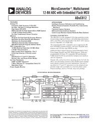
ADuC812 MicroConverter Parallel Programming Specification
ADuC812 MicroConverter Parallel Programming Specification
ADuC812 MicroConverter Parallel Programming Specification

Create successful ePaper yourself
Turn your PDF publications into a flip-book with our unique Google optimized e-Paper software.
a<br />
<strong>ADuC812</strong> <strong>MicroConverter</strong> ®<br />
<strong>Parallel</strong> <strong>Programming</strong> <strong>Specification</strong><br />
Version 1.3<br />
10 July 2001<br />
This document details device configuration and timing specifications required to program the Flash/EE<br />
Memory of the <strong>ADuC812</strong> <strong>MicroConverter</strong> in parallel programming mode. The <strong>ADuC812</strong> datasheet<br />
includes other necessary product information not offered in this document. It can be found at<br />
http://www.analog.com/microconverter.<br />
Note that parallel programming mode is only one of two methods to program the <strong>ADuC812</strong>. For details<br />
on the in-circuit serial download mode, refer to the <strong>ADuC812</strong> datasheet and tech note uC004, both<br />
available at http://www.analog.com/microconverter.<br />
Rise & Fall times on all timing diagrams in this document are specified as 10ns min / 100ns max.<br />
All timing parameters are measured from the 50% level on a given signal.<br />
CONTENTS:<br />
Section:<br />
Page:<br />
Pin Configuration 2<br />
Power-Up & Power-Down Sequences 3<br />
Memory Map 4<br />
Command Functions 4<br />
Read Device Signature 5<br />
Read Byte 6<br />
Erase All 7<br />
Program Byte 8<br />
Program Page 9<br />
<strong>ADuC812</strong> <strong>Parallel</strong> <strong>Programming</strong> Spec. V1.3 Page 1 of 9
Pin Configuration<br />
The basic pin configuration for parallel programming is shown in Figure 1. The specific function of each<br />
pin and port is outlined below.<br />
• Port 0: 8-bit bi-directional DATA BUS for programming and reading bytes<br />
• Ports 1 & 2: 16-bit ADDRESS BUS input (Port 1 is the high-byte, Port 2 is the low-byte)<br />
• P3.1-P3.7: 7-bit COMMAND input, for specifying erase, program, read, etc.<br />
• P3.0: active-low ENABLE COMMAND input for strobing a command on P3.1-P3.7<br />
• ALE: active-low WRITE ENABLE input, used in programming functions<br />
• EA : active-high ENABLE HV input, enables on-chip high-voltage charge-pump when high<br />
• XTAL1: STROBE CONFIG input, used to latch the chip into parallel programming mode<br />
• PSEN : MODE SELECT input, used with XTAL1 to select parallel programming mode<br />
• RESET: this pin must remain at the same potential as the VDD pins at all times<br />
+5V<br />
+5V<br />
5<br />
20<br />
34<br />
48<br />
ENABLE HV<br />
WRITE ENABLE<br />
15<br />
40<br />
42<br />
RESET<br />
EA<br />
ALE<br />
AVDD<br />
DVDD<br />
DVDD<br />
DVDD<br />
PORT 0<br />
43<br />
44<br />
45<br />
46<br />
49<br />
50<br />
51<br />
52<br />
LSB<br />
MSB<br />
DATA<br />
ENABLE CMD<br />
LSB<br />
COMMAND<br />
MSB<br />
STROBE CONFIG<br />
MODE SELECT<br />
16<br />
17<br />
18<br />
19<br />
22<br />
23<br />
24<br />
25<br />
41<br />
P3.0<br />
32 XTAL1<br />
PSEN<br />
P3.1 - P3.7<br />
AGND<br />
<strong>ADuC812</strong><br />
28<br />
29<br />
30<br />
31<br />
36<br />
37<br />
38<br />
39<br />
1<br />
2<br />
3<br />
4<br />
11<br />
12<br />
13<br />
14<br />
6<br />
21<br />
35<br />
47<br />
DGND<br />
DGND<br />
DGND<br />
PORT 2<br />
PORT 1<br />
LSB<br />
ADDRESS<br />
MSB<br />
Figure 1: Pin Configuration for <strong>Parallel</strong> <strong>Programming</strong><br />
<strong>ADuC812</strong> <strong>Parallel</strong> <strong>Programming</strong> Spec. V1.3 Page 2 of 9
Power-Up & Power-Down Sequences<br />
There are a number of requirements for correct application and removal of power for parallel<br />
programming mode. They are outlined in the below bullets and further details are illustrated in Figure 2.<br />
• All four ground pins (DGND & AGND) must be treated as a single node.<br />
• All four VDD pins (AVDD & DVDD) plus the RESET pin must all be treated as a single node.<br />
• The voltage applied to any pin must never be greater than VDD or less than ground.<br />
• Any time power is applied to the chip all signals must meet the requirements of Figure 2.<br />
• During the “Command Sequences” section of Figure 2, the following reqirements must be met....<br />
− VDD and RESET must remain high.<br />
− PSEN must remain low.<br />
− XTAL1 must remain low.<br />
− ALE and P3.0 must remain high, except when pulsed low during specific command sequences.<br />
− EA must remain low, except when pulsed high during specific command sequences.<br />
Power-Up<br />
Sequence<br />
any number of<br />
Command Sequences<br />
(on following pages)<br />
Power-Down<br />
Sequence<br />
AVDD / DVDD / RESET (I)<br />
PSEN = MODE SELECT (I)<br />
1µs min<br />
1µs min<br />
ALE = WRITE ENABLE (I)<br />
10µs min<br />
EA = ENABLE HV (I)<br />
P3.0 = ENABLE CMD (I)<br />
P3.7-P3.1 = COMMAND (I)<br />
50ms min<br />
20µs<br />
min<br />
20µs<br />
min<br />
XTAL1 = STROBE CONFIG * (I)<br />
* The <strong>ADuC812</strong> enters parallel programming mode on the 1st rising edge of STROBE CONFIG (XTAL1) in the above diagram.<br />
Figure 2: Power-Up & Power-Down Sequences for <strong>Parallel</strong> <strong>Programming</strong><br />
<strong>ADuC812</strong> <strong>Parallel</strong> <strong>Programming</strong> Spec. V1.3 Page 3 of 9
Memory Map<br />
In parallel programming mode, the various areas of the <strong>ADuC812</strong>’s internal Flash/EE memory are<br />
mapped into portions of the 64K byte addressable space as shown in Figure 3.<br />
FFFF hex<br />
3-byte Device Signature<br />
F8FD hex<br />
F8FC hex<br />
F8FB hex<br />
64K bytes<br />
Total Addressable<br />
in <strong>Parallel</strong><br />
<strong>Programming</strong> Mode<br />
640 bytes<br />
On-Chip Flash/EE<br />
Data Memory<br />
F680 hex<br />
F67F hex<br />
F400 hex<br />
F3FF hex<br />
2000 hex<br />
1FFF hex<br />
8K bytes<br />
On-Chip Flash/EE<br />
Program Memory<br />
0000 hex<br />
Figure 3: <strong>Parallel</strong> <strong>Programming</strong> Memory Map<br />
Command Functions<br />
The commands used to carry out various parallel programming functions are listed below.<br />
P3.7 P3.6 P3.5 P3.4 P3.3 P3.2 P3.1 Function Page<br />
1 1 1 1 1 1 1 default pullups – do nothing –<br />
1 1 1 1 0 0 0 ERASE ALL (code/data plus security bits) 7<br />
1 1 1 1 0 0 1 READ DEVICE SIGNATURE 5<br />
1 1 1 1 0 1 0 PROGRAM BYTE 8<br />
1 1 1 1 0 1 1 READ BYTE 6<br />
all others reserved –<br />
Each of the above command functions is described in detail on the following pages.<br />
<strong>ADuC812</strong> <strong>Parallel</strong> <strong>Programming</strong> Spec. V1.3 Page 4 of 9
Read Device Signature<br />
Command Key:<br />
P3.7 P3.6 P3.5 P3.4 P3.3 P3.2 P3.1 Function<br />
1 1 1 1 0 0 1 READ DEVICE SIGNATURE<br />
You can read the device signature to ensure that the device inserted in the programmer is in fact an<br />
<strong>ADuC812</strong>. To do so, follow the timing shown in Figure 4, and read back addresses F8FB, F8FC, and<br />
F8FD hex. They should read back as the ASCII characters ‘8’, ‘1’, and ‘2’ respectively, as shown in the<br />
below table. Using this command to read any addresses other than the three given below will return<br />
undefined results.<br />
Device Signature Read-Back Values:<br />
Address (hex) Value (hex/dec/ASCII)<br />
F8FB hex 38 hex / 56 dec / ‘8’<br />
F8FC hex 31 hex / 49 dec / ‘1’<br />
F8FD hex 32 hex / 50 dec / ‘2’<br />
P3.7 - P3.1 = COMMAND (I)<br />
COMMAND<br />
Ports 1 & 2 = ADDRESS (I)<br />
BYTE ADDRESS<br />
Port 0 = DATA (O)<br />
DATA<br />
ALE = WRITE ENABLE (I)<br />
(high)<br />
EA = ENABLE HV (I)<br />
(low)<br />
0µs min<br />
P3.0 = ENABLE CMD (I)<br />
1µs min 1µs max<br />
100ns min<br />
Figure 4: Read Device Signature Timing<br />
<strong>ADuC812</strong> <strong>Parallel</strong> <strong>Programming</strong> Spec. V1.3 Page 5 of 9
Read Byte<br />
Command Key:<br />
P3.7 P3.6 P3.5 P3.4 P3.3 P3.2 P3.1 Function<br />
1 1 1 1 0 1 1 READ BYTE<br />
To read data, one byte at a time, from the <strong>ADuC812</strong>, follow the timing shown in Figure 5.<br />
P3.7 - P3.1 = COMMAND (I)<br />
COMMAND<br />
Ports 1 & 2 = ADDRESS (I)<br />
BYTE ADDRESS<br />
Port 0 = DATA (O)<br />
DATA<br />
ALE = WRITE ENABLE (I)<br />
(high)<br />
EA = ENABLE HV (I)<br />
(low)<br />
0µs min<br />
P3.0 = ENABLE CMD (I)<br />
1µs min 1µs max<br />
100ns min<br />
Figure 5: Read Byte Timing<br />
<strong>ADuC812</strong> <strong>Parallel</strong> <strong>Programming</strong> Spec. V1.3 Page 6 of 9
Erase All<br />
Command Key:<br />
P3.7 P3.6 P3.5 P3.4 P3.3 P3.2 P3.1 Function<br />
1 1 1 1 0 0 0 ERASE ALL (code/data memory)<br />
To erase the Flash/EE memory of the <strong>ADuC812</strong>, follow the timing given in Figure 6. This will erase the<br />
following areas....<br />
• 8K byte Program Space<br />
• 640 byte Data Space<br />
P3.7 - P3.1 = COMMAND (I)<br />
COMMAND<br />
ALE = WRITE ENABLE (I)<br />
(high)<br />
10µs min<br />
10µs min<br />
EA = ENABLE HV (I)<br />
10µs min<br />
P3.0 = ENABLE CMD (I)<br />
20ms±1ms<br />
30µs min<br />
Figure 6: Erase All Timing<br />
<strong>ADuC812</strong> <strong>Parallel</strong> <strong>Programming</strong> Spec. V1.3 Page 7 of 9
Program Byte<br />
Command Key:<br />
P3.7 P3.6 P3.5 P3.4 P3.3 P3.2 P3.1 Function<br />
1 1 1 1 0 1 0 PROGRAM BYTE<br />
To program the <strong>ADuC812</strong>’s program or data memory, one byte at a time, follow the timing shown in<br />
Figure 7.<br />
P3.7 - P3.1 = COMMAND (I)<br />
COMMAND<br />
Ports 1 & 2 = ADDRESS (I)<br />
BYTE ADDRESS<br />
Port 0 = DATA (I)<br />
DATA<br />
30µs±5µs<br />
ALE = WRITE ENABLE (I)<br />
1µs min<br />
1µs min<br />
EA = ENABLE HV (I)<br />
10µs±1µs<br />
P3.0 = ENABLE CMD (I)<br />
10µs±1µs<br />
60µs±10µs<br />
10µs min<br />
Figure 7: Program Byte Timing<br />
<strong>ADuC812</strong> <strong>Parallel</strong> <strong>Programming</strong> Spec. V1.3 Page 8 of 9
Program Page<br />
Command Key:<br />
P3.7 P3.6 P3.5 P3.4 P3.3 P3.2 P3.1 Function<br />
1 1 1 1 0 1 0 PROGRAM BYTE<br />
As an alternative to programming the <strong>ADuC812</strong> a single byte at a time as in Figure 7, you can instead<br />
choose to utilise the page-programming function by following the timing shown in Figure 8. Note that<br />
the command byte is exactly the same as for a byte programming function, and in fact the page<br />
programming function is little more than a series of consecutive single bytes programmed in quick<br />
succession within strict timing constraints. If for any reason you cannot meet all the timing requirements<br />
of Figure 8, then use byte programming instead.<br />
A page of program memory is 32 bytes in size, whereas a page of data memory is only 2 bytes in size*.<br />
For program memory, the first address of a page ends in the bits 00000, and the last address of a page<br />
ends in the bits 11111. For data memory, the first address of a page ends in a 0 bit, and the second (i.e.<br />
last) address in a page ends in a 1 bit. This is illustrated in the tables below. Page programming of the<br />
<strong>ADuC812</strong> requires that all addresses in the page be programmed sequentially within a single sequence,<br />
starting with Address 0 and ending with Address 31 (or Address 1 for data memory).<br />
One Page of Program Memory<br />
One Page of Data Memory*<br />
Address 0 XXXXXXXXXX00000 Address 0 XXXXXXXXXXXXXXX0<br />
Address 1 XXXXXXXXXX00001 Address 1 XXXXXXXXXXXXXXX1<br />
Address 2 XXXXXXXXXX00010<br />
... ...<br />
* In <strong>Parallel</strong> <strong>Programming</strong> Mode a page<br />
Address 31 XXXXXXXXXX11111<br />
of Data Memory is 2 bytes, whereas in<br />
User Mode each page is 4 bytes.<br />
P3.7 - P3.1 = COMMAND (I)<br />
COMMAND<br />
Ports 1 & 2 = ADDRESS (I)<br />
ADDRESS 0<br />
5µs min<br />
1 2 31<br />
5µs min<br />
Port 0 = DATA (I)<br />
DATA 0<br />
1 2<br />
31<br />
30µs±5µs<br />
ALE = WRITE ENABLE (I)<br />
10µs±1µs<br />
10µs±1µs<br />
1µs min<br />
EA = ENABLE HV (I)<br />
P3.0 = ENABLE CMD (I)<br />
1µs min<br />
60µs±10µs<br />
10µs±1µs<br />
10µs min<br />
Figure 8: Program Page Timing<br />
<strong>ADuC812</strong> <strong>Parallel</strong> <strong>Programming</strong> Spec. V1.3 Page 9 of 9