ADuC812 MicroConverter, Multichannel 12-bit ADC with Embedded ...
ADuC812 MicroConverter, Multichannel 12-bit ADC with Embedded ...
ADuC812 MicroConverter, Multichannel 12-bit ADC with Embedded ...

Create successful ePaper yourself
Turn your PDF publications into a flip-book with our unique Google optimized e-Paper software.
a<br />
FEATURES<br />
Analog I/O<br />
8-Channel, High Accuracy <strong>12</strong>-Bit <strong>ADC</strong><br />
On-Chip, 100 ppm/C Voltage Reference<br />
High Speed 200 kSPS<br />
DMA Controller for High Speed <strong>ADC</strong>-to-RAM Capture<br />
2 <strong>12</strong>-Bit Voltage Output DACs<br />
On-Chip Temperature Sensor Function<br />
Memory<br />
8K Bytes On-Chip Flash/EE Program Memory<br />
640 Bytes On-Chip Flash/EE Data Memory<br />
256 Bytes On-Chip Data RAM<br />
16M Bytes External Data Address Space<br />
64K Bytes External Program Address Space<br />
8051 Compatible Core<br />
<strong>12</strong> MHz Nominal Operation (16 MHz Max)<br />
3 16-Bit Timer/Counters<br />
High Current Drive Capability—Port 3<br />
9 Interrupt Sources, 2 Priority Levels<br />
Power<br />
Specified for 3 V and 5 V Operation<br />
Normal, Idle, and Power-Down Modes<br />
On-Chip Peripherals<br />
UART and SPI ® Serial I/O<br />
2-Wire (400 kHz I 2 C ® Compatible) Serial I/O<br />
Watchdog Timer<br />
Power Supply Monitor<br />
<strong>MicroConverter</strong> ® , <strong>Multichannel</strong><br />
<strong>12</strong>-Bit <strong>ADC</strong> <strong>with</strong> <strong>Embedded</strong> Flash MCU<br />
<strong>ADuC8<strong>12</strong></strong><br />
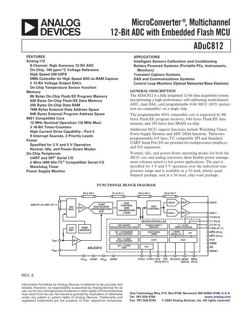
FUNCTIONAL BLOCK DIAGRAM<br />
APPLICATIONS<br />
Intelligent Sensors Calibration and Conditioning<br />
Battery-Powered Systems (Portable PCs, Instruments,<br />
Monitors)<br />
Transient Capture Systems<br />
DAS and Communications Systems<br />
Control Loop Monitors (Optical Networks/Base Stations)<br />
GENERAL DESCRIPTION<br />
The <strong>ADuC8<strong>12</strong></strong> is a fully integrated <strong>12</strong>-<strong>bit</strong> data acquisition system<br />
incorporating a high performance self-calibrating multichannel<br />
<strong>ADC</strong>, dual DAC, and programmable 8-<strong>bit</strong> MCU (8051 instruction<br />
set compatible) on a single chip.<br />
The programmable 8051 compatible core is supported by 8K<br />
bytes Flash/EE program memory, 640 bytes Flash/EE data<br />
memory, and 256 bytes data SRAM on-chip.<br />
Additional MCU support functions include Watchdog Timer,<br />
Power Supply Monitor, and <strong>ADC</strong> DMA functions. Thirty-two<br />
programmable I/O lines, I 2 C compatible SPI and Standard<br />
UART Serial Port I/O are provided for multiprocessor interfaces<br />
and I/O expansion.<br />
Normal, idle, and power-down operating modes for both the<br />
MCU core and analog converters allow flexible power management<br />
schemes suited to low power applications. The part is<br />
specified for 3 V and 5 V operation over the industrial temperature<br />
range and is available in a 52-lead, plastic quad<br />
flatpack package, and in a 56-lead, chip scale package.<br />
P0.0–P0.7<br />
P1.0–P1.7<br />
P2.0–P2.7<br />
P3.0–P3.7<br />
AIN0 (P1.0)–AIN7 (P1.7)<br />
AIN<br />
MUX<br />
T/H<br />
<strong>12</strong>-BIT<br />
SUCCESSIVE<br />
APPROXIMATION<br />
<strong>ADC</strong><br />
<strong>ADC</strong><br />
CONTROL<br />
AND<br />
CALIBRATION<br />
LOGIC<br />
DAC<br />
CONTROL<br />
DAC0<br />
DAC1<br />
BUF<br />
BUF<br />
DAC0<br />
DAC1<br />
T0 (P3.4)<br />
V REF<br />
C REF<br />
2.5V<br />
REF<br />
BUF<br />
TEMP<br />
SENSOR<br />
<strong>ADuC8<strong>12</strong></strong><br />
8051 BASED<br />
MICROCONTROLLER CORE<br />
8K 8 PROGRAM<br />
FLASH EEPROM<br />
640 8 USER<br />
FLASH EEPROM<br />
256 8 USER<br />
RAM<br />
MICROCONTROLLER<br />
POWER SUPPLY<br />
MONITOR<br />
OSC<br />
WATCHDOG<br />
TIMER<br />
UART<br />
3 16-BIT<br />
TIMER/COUNTERS<br />
2-WIRE<br />
SERIAL I/O<br />
MUX<br />
SPI<br />
T1 (P3.5)<br />
T2 (P1.0)<br />
T2EX (P1.1)<br />
INT0 (P3.2)<br />
INT1 (P3.3)<br />
ALE<br />
PSEN<br />
EA<br />
RESET<br />
AV DD<br />
AGND<br />
DV DD<br />
DGND<br />
XTAL1 XTAL2 RxD TxD<br />
(P3.0) (P3.1)<br />
SCLOCK MOSI/<br />
SDATA<br />
MISO<br />
(P3.3)<br />
REV. E<br />
Information furnished by Analog Devices is believed to be accurate and<br />
reliable. However, no responsibility is assumed by Analog Devices for its<br />
use, nor for any infringements of patents or other rights of third parties that<br />
may result from its use. No license is granted by implication or otherwise<br />
under any patent or patent rights of Analog Devices. Trademarks and<br />
registered trademarks are the property of their respective companies.<br />
One Technology Way, P.O. Box 9106, Norwood, MA 02062-9106, U.S.A.<br />
Tel: 781/329-4700<br />
www.analog.com<br />
Fax: 781/326-8703 © 2003 Analog Devices, Inc. All rights reserved.
<strong>ADuC8<strong>12</strong></strong><br />
TABLE OF CONTENTS<br />
FEATURES . . . . . . . . . . . . . . . . . . . . . . . . . . . . . . . . . . . . . . . . 1<br />
APPLICATONS . . . . . . . . . . . . . . . . . . . . . . . . . . . . . . . . . . . . . 1<br />
GENERAL DESCRIPTION . . . . . . . . . . . . . . . . . . . . . . . . . . . 1<br />
SPECIFICATIONS . . . . . . . . . . . . . . . . . . . . . . . . . . . . . . . . . . 3<br />
ABSOLUTE MAXIMUM RATINGS . . . . . . . . . . . . . . . . . . . . 6<br />
PIN CONFIGURATIONS . . . . . . . . . . . . . . . . . . . . . . . . . . . . . 6<br />
ORDERING GUIDE . . . . . . . . . . . . . . . . . . . . . . . . . . . . . . . . . 6<br />
PIN FUNCTION DESCRIPTIONS . . . . . . . . . . . . . . . . . . . . . 7<br />
TERMINOLOGY . . . . . . . . . . . . . . . . . . . . . . . . . . . . . . . . . . . . 8<br />
<strong>ADC</strong> SPECIFICATIONS . . . . . . . . . . . . . . . . . . . . . . . . . . . . . . 8<br />
Integral Nonlinearity . . . . . . . . . . . . . . . . . . . . . . . . . . . . . . . . 8<br />
Differential Nonlinearity . . . . . . . . . . . . . . . . . . . . . . . . . . . . . 8<br />
Offset Error . . . . . . . . . . . . . . . . . . . . . . . . . . . . . . . . . . . . . . . 8<br />
Full-Scale Error . . . . . . . . . . . . . . . . . . . . . . . . . . . . . . . . . . . . 8<br />
Signal to (Noise + Distortion) Ratio . . . . . . . . . . . . . . . . . . . . 8<br />
Total Harmonic Distortion . . . . . . . . . . . . . . . . . . . . . . . . . . . 8<br />
DAC SPECIFICATIONS . . . . . . . . . . . . . . . . . . . . . . . . . . . . . . 8<br />
Relative Accuracy . . . . . . . . . . . . . . . . . . . . . . . . . . . . . . . . . . . 8<br />
Voltage Output Settling Time . . . . . . . . . . . . . . . . . . . . . . . . . 8<br />
Digital-to-Analog Glitch Impulse . . . . . . . . . . . . . . . . . . . . . . . 8<br />
ARCHITECTURE, MAIN FEATURES . . . . . . . . . . . . . . . . . . 9<br />
MEMORY ORGANIZATION . . . . . . . . . . . . . . . . . . . . . . . . . . 9<br />
OVERVIEW OF MCU-RELATED SFRs . . . . . . . . . . . . . . . . . 10<br />
Accumulator SFR . . . . . . . . . . . . . . . . . . . . . . . . . . . . . . . . . 10<br />
B SFR . . . . . . . . . . . . . . . . . . . . . . . . . . . . . . . . . . . . . . . . . . 10<br />
Stack Pointer SFR . . . . . . . . . . . . . . . . . . . . . . . . . . . . . . . . . 10<br />
Data Pointer . . . . . . . . . . . . . . . . . . . . . . . . . . . . . . . . . . . . . 10<br />
Program Status Word SFR . . . . . . . . . . . . . . . . . . . . . . . . . . . 10<br />
Power Control SFR . . . . . . . . . . . . . . . . . . . . . . . . . . . . . . . . 10<br />
SPECIAL FUNCTION REGISTERS . . . . . . . . . . . . . . . . . . . 11<br />
<strong>ADC</strong> CIRCUIT INFORMATION . . . . . . . . . . . . . . . . . . . . . . <strong>12</strong><br />
General Overview . . . . . . . . . . . . . . . . . . . . . . . . . . . . . . . . . . <strong>12</strong><br />
<strong>ADC</strong> Transfer Function . . . . . . . . . . . . . . . . . . . . . . . . . . . . . <strong>12</strong><br />
Typical Operation . . . . . . . . . . . . . . . . . . . . . . . . . . . . . . . . . <strong>12</strong><br />
<strong>ADC</strong>CON1—(<strong>ADC</strong> Control SFR #1) . . . . . . . . . . . . . . . . . 13<br />
<strong>ADC</strong>CON2—(<strong>ADC</strong> Control SFR #2) . . . . . . . . . . . . . . . . . 14<br />
<strong>ADC</strong>CON3—(<strong>ADC</strong> Control SFR #3) . . . . . . . . . . . . . . . . . 14<br />
Driving the <strong>ADC</strong> . . . . . . . . . . . . . . . . . . . . . . . . . . . . . . . . . . 15<br />
Voltage Reference Connections . . . . . . . . . . . . . . . . . . . . . . . 16<br />
Configuring the <strong>ADC</strong> . . . . . . . . . . . . . . . . . . . . . . . . . . . . . . . 16<br />
<strong>ADC</strong> DMA Mode . . . . . . . . . . . . . . . . . . . . . . . . . . . . . . . . . 16<br />
DMA Mode Configuration Example . . . . . . . . . . . . . . . . . . . 17<br />
Micro Operation during <strong>ADC</strong> DMA Mode . . . . . . . . . . . . . . 17<br />
Offset and Gain Calibration Coefficients . . . . . . . . . . . . . . . . 17<br />
Calibration . . . . . . . . . . . . . . . . . . . . . . . . . . . . . . . . . . . . . . . 18<br />
NONVOLATILE FLASH MEMORY . . . . . . . . . . . . . . . . . . . 18<br />
Flash Memory Overview . . . . . . . . . . . . . . . . . . . . . . . . . . . . 18<br />
Flash/EE Memory and the <strong>ADuC8<strong>12</strong></strong> . . . . . . . . . . . . . . . . . . 18<br />
<strong>ADuC8<strong>12</strong></strong> Flash/EE Memory Reliability . . . . . . . . . . . . . . . . 18<br />
Using the Flash/EE Program Memory . . . . . . . . . . . . . . . . . . 19<br />
Using the Flash/EE Data Memory . . . . . . . . . . . . . . . . . . . . . 19<br />
ECON—Flash/EE Memory Control SFR . . . . . . . . . . . . . . . 20<br />
Flash/EE Memory Timing . . . . . . . . . . . . . . . . . . . . . . . . . . . 20<br />
Using the Flash/EE Memory Interface . . . . . . . . . . . . . . . . . . 20<br />
Erase-All . . . . . . . . . . . . . . . . . . . . . . . . . . . . . . . . . . . . . . . . 20<br />
Program a Byte . . . . . . . . . . . . . . . . . . . . . . . . . . . . . . . . . . . 20<br />
USER INTERFACE TO OTHER ON-CHIP<br />
<strong>ADuC8<strong>12</strong></strong> PERIPHERALS . . . . . . . . . . . . . . . . . . . . . . . . . . . . 21<br />
Using the DAC . . . . . . . . . . . . . . . . . . . . . . . . . . . . . . . . . . . 22<br />
WATCHDOG TIMER . . . . . . . . . . . . . . . . . . . . . . . . . . . . . . . 24<br />
POWER SUPPLY MONITOR . . . . . . . . . . . . . . . . . . . . . . . . . 24<br />
SERIAL PERIPHERAL INTERFACE . . . . . . . . . . . . . . . . . . . 25<br />
MISO (Master In, Slave Out Data I/O Pin) . . . . . . . . . . . . . . 25<br />
MOSI (Master Out, Slave In Pin) . . . . . . . . . . . . . . . . . . . . . 26<br />
SCLOCK (Serial Clock I/O Pin) . . . . . . . . . . . . . . . . . . . . . . 26<br />
SS (Slave Select Input Pin) . . . . . . . . . . . . . . . . . . . . . . . . . . 26<br />
Using the SPI Interface . . . . . . . . . . . . . . . . . . . . . . . . . . . . . 27<br />
SPI Interface—Master Mode . . . . . . . . . . . . . . . . . . . . . . . . . 27<br />
SPI Interface—Slave Mode . . . . . . . . . . . . . . . . . . . . . . . . . . 27<br />
I 2 C COMPATIBLE INTERFACE . . . . . . . . . . . . . . . . . . . . . . 28<br />
8051 COMPATIBLE ON-CHIP PERIPHERALS . . . . . . . . . . 29<br />
Parallel I/O Ports 0–3 . . . . . . . . . . . . . . . . . . . . . . . . . . . . . . . 29<br />
Timers/Counters . . . . . . . . . . . . . . . . . . . . . . . . . . . . . . . . . . 29<br />
Timer/Counters 0 and 1 Data Registers . . . . . . . . . . . . . . . . . 31<br />
TH0 and TL0 . . . . . . . . . . . . . . . . . . . . . . . . . . . . . . . . . . . . 31<br />
TH1 and TL1 . . . . . . . . . . . . . . . . . . . . . . . . . . . . . . . . . . . . 31<br />
TIMER/COUNTERS 0 AND 1 OPERATING MODES . . . . . 32<br />
Mode 0 (13-Bit Timer/Counter) . . . . . . . . . . . . . . . . . . . . . . 32<br />
Mode 1 (16-Bit Timer/Counter) . . . . . . . . . . . . . . . . . . . . . . 32<br />
Mode 2 (8-Bit Timer/Counter <strong>with</strong> Auto Reload) . . . . . . . . . 32<br />
Mode 3 (Two 8-Bit Timer/Counters) . . . . . . . . . . . . . . . . . . 32<br />
Timer/Counter 2 Data Registers . . . . . . . . . . . . . . . . . . . . . . 33<br />
TH2 and TL2 . . . . . . . . . . . . . . . . . . . . . . . . . . . . . . . . . . . . 33<br />
RCAP2H and RCAP2L . . . . . . . . . . . . . . . . . . . . . . . . . . . . . 33<br />
Timer/Counter Operation Modes . . . . . . . . . . . . . . . . . . . . . 34<br />
16-Bit Autoreload Mode . . . . . . . . . . . . . . . . . . . . . . . . . . . . 34<br />
16-Bit Capture Mode . . . . . . . . . . . . . . . . . . . . . . . . . . . . . . . 34<br />
UART SERIAL INTERFACE . . . . . . . . . . . . . . . . . . . . . . . . . 35<br />
Mode 0 (8-Bit Shift Register Mode) . . . . . . . . . . . . . . . . . . . 36<br />
Mode 1 (8-Bit UART, Variable Baud Rate) . . . . . . . . . . . . . . 36<br />
Mode 2 (9-Bit UART <strong>with</strong> Fixed Baud Rate) . . . . . . . . . . . . 36<br />
Mode 3 (9-Bit UART <strong>with</strong> Variable Baud Rate) . . . . . . . . . . 36<br />
UART Serial Port Baud Rate Generation . . . . . . . . . . . . . . . 36<br />
Timer 1 Generated Baud Rates . . . . . . . . . . . . . . . . . . . . . . . 37<br />
Timer 2 Generated Baud Rates . . . . . . . . . . . . . . . . . . . . . . . 37<br />
INTERRUPT SYSTEM . . . . . . . . . . . . . . . . . . . . . . . . . . . . . . 38<br />
Interrupt Priority . . . . . . . . . . . . . . . . . . . . . . . . . . . . . . . . . . 39<br />
Interrupt Vectors . . . . . . . . . . . . . . . . . . . . . . . . . . . . . . . . . . 39<br />
<strong>ADuC8<strong>12</strong></strong> HARDWARE DESIGN CONSIDERATIONS . . . . 40<br />
Clock Oscillator . . . . . . . . . . . . . . . . . . . . . . . . . . . . . . . . . . . 40<br />
External Memory Interface . . . . . . . . . . . . . . . . . . . . . . . . . . 40<br />
Power-On Reset Operation . . . . . . . . . . . . . . . . . . . . . . . . . . 41<br />
Power Supplies . . . . . . . . . . . . . . . . . . . . . . . . . . . . . . . . . . . . 41<br />
Power Consumption . . . . . . . . . . . . . . . . . . . . . . . . . . . . . . . 42<br />
Grounding and Board Layout Recommendations . . . . . . . . . 43<br />
OTHER HARDWARE CONSIDERATIONS . . . . . . . . . . . . . 44<br />
In-Circuit Serial Download Access . . . . . . . . . . . . . . . . . . . . 44<br />
<strong>Embedded</strong> Serial Port Debugger . . . . . . . . . . . . . . . . . . . . . . 44<br />
Single-Pin Emulation Mode . . . . . . . . . . . . . . . . . . . . . . . . . . 45<br />
Enhanced-Hooks Emulation Mode . . . . . . . . . . . . . . . . . . . . 45<br />
Typical System Configuration . . . . . . . . . . . . . . . . . . . . . . . . 45<br />
QUICKSTART DEVELOPMENT SYSTEM . . . . . . . . . . . . . 45<br />
Download—In-Circuit Serial Downloader . . . . . . . . . . . . . . . 45<br />
DeBug—In-Circuit Debugger . . . . . . . . . . . . . . . . . . . . . . . . 45<br />
ADSIM—Windows Simulator . . . . . . . . . . . . . . . . . . . . . . . . 45<br />
TIMING SPECIFICATIONS . . . . . . . . . . . . . . . . . . . . . . . . . 46<br />
OUTLINE DIMENSIONS . . . . . . . . . . . . . . . . . . . . . . . . . . . . 56<br />
Revision History . . . . . . . . . . . . . . . . . . . . . . . . . . . . . . . . . . . . 57<br />
–2–<br />
REV. E
<strong>ADuC8<strong>12</strong></strong><br />
SPECIFICATIONS 1, 2 (AV DD = DV DD = 3.0 V or 5.0 V 10%, REF IN /REF OUT = 2.5 V Internal Reference, MCLKIN = 11.0592 MHz,<br />
f SAMPLE = 200 kHz, DAC V OUT Load to AGND; R L = 2 k, C L = 100 pF. All specifications T A = T MIN to T MAX , unless otherwise noted.)<br />
<strong>ADuC8<strong>12</strong></strong>BS<br />
Parameter V DD = 5 V V DD = 3 V Unit Test Conditions/Comments<br />
<strong>ADC</strong> CHANNEL SPECIFICATIONS<br />
DC ACCURACY 3, 4<br />
Resolution <strong>12</strong> <strong>12</strong> Bits<br />
Integral Nonlinearity ±1/2 ±1/2 LSB typ f SAMPLE = 100 kHz<br />
±1.5 ±1.5 LSB max f SAMPLE = 100 kHz<br />
±1.5 ±1.5 LSB typ f SAMPLE = 200 kHz<br />
Differential Nonlinearity ±1 ±1 LSB typ f SAMPLE = 100 kHz. Guaranteed No<br />
Missing Codes at 5 V<br />
CALIBRATED ENDPOINT ERRORS 5, 6<br />
Offset Error ±5 ±5 LSB max<br />
±1 ±1 LSB typ<br />
Offset Error Match 1 1 LSB typ<br />
Gain Error ±6 ±6 LSB max<br />
±1 ±1 LSB typ<br />
Gain Error Match 1.5 1.5 LSB typ<br />
USER SYSTEM CALIBRATION 7<br />
Offset Calibration Range ±5 ±5 % of V REF typ<br />
Gain Calibration Range ±2.5 ±2.5 % of V REF typ<br />
DYNAMIC PERFORMANCE<br />
Signal-to-Noise Ratio (SNR) 8 70 70 dB typ<br />
Total Harmonic Distortion (THD) –78 –78 dB typ<br />
Peak Harmonic or Spurious Noise –78 –78 dB typ<br />
ANALOG INPUT<br />
Input Voltage Ranges 0 to V REF 0 to V REF V<br />
Leakage Current ±1 ±1 µA max<br />
±0.1 ±0.1 µA typ<br />
Input Capacitance 9 20 20 pF max<br />
f IN = 10 kHz Sine Wave<br />
f SAMPLE = 100 kHz<br />
TEMPERATURE SENSOR 10<br />
Voltage Output at 25°C 600 600 mV typ Can vary significantly (> ±20%)<br />
Voltage TC –3.0 –3.0 mV/°C typ from device to device<br />
DAC CHANNEL SPECIFICATIONS<br />
DC ACCURACY 11<br />
Resolution <strong>12</strong> <strong>12</strong> Bits<br />
Relative Accuracy ±3 ±3 LSB typ<br />
Differential Nonlinearity ±0.5 ±1 LSB typ Guaranteed <strong>12</strong>-Bit Monotonic<br />
Offset Error ±60 ±60 mV max<br />
±15 ±15 mV typ<br />
Full-Scale Error ±30 ±30 mV max<br />
±10 ±10 mV typ<br />
Full-Scale Mismatch ±0.5 ±0.5 % typ % of Full-Scale on DAC1<br />
ANALOG OUTPUTS<br />
Voltage Range_0 0 to V REF 0 to V REF V typ<br />
Voltage Range_1 0 to V DD 0 to V DD V typ<br />
Resistive Load 10 10 kΩ typ<br />
Capacitive Load 100 100 pF typ<br />
Output Impedance 0.5 0.5 Ω typ<br />
I SINK 50 50 µA typ<br />
REV. E –3–
<strong>ADuC8<strong>12</strong></strong><br />
SPECIFICATIONS 1, 2 (continued)<br />
<strong>ADuC8<strong>12</strong></strong>BS<br />
Parameter V DD = 5 V V DD = 3 V Unit Test Conditions/Comments<br />
DAC AC CHARACTERISTICS<br />
Voltage Output Settling Time 15 15 µs typ Full-Scale Settling Time to<br />
<strong>with</strong>in 1/2 LSB of Final Value<br />
Digital-to-Analog Glitch Energy 10 10 nV sec typ 1 LSB Change at Major Carry<br />
REFERENCE INPUT/OUTPUT<br />
REF IN Input Voltage Range 9 2.3/V DD 2.3/V DD V min/max<br />
Input Impedance 150 150 kΩ typ<br />
REF OUT Output Voltage 2.5 ± 2.5% 2.5 ± 2.5% V min/max Initial Tolerance @ 25°C<br />
2.5 2.5 V typ<br />
REF OUT Tempco 100 100 ppm/°C typ<br />
FLASH/EE MEMORY PERFORMANCE<br />
<strong>12</strong>, 13<br />
CHARACTERISTICS<br />
Endurance 10,000 Cycles min<br />
50,000 50,000 Cycles typ<br />
Data Retention 10 Years min<br />
WATCHDOG TIMER<br />
CHARACTERISTICS<br />
Oscillator Frequency 64 64 kHz typ<br />
POWER SUPPLY MONITOR<br />
CHARACTERISTICS<br />
Power Supply Trip Point Accuracy ±2.5 ±2.5 % of Selected<br />
Nominal Trip<br />
Point Voltage<br />
max<br />
±1.0 ±1.0 % of Selected<br />
Nominal Trip<br />
Point Voltage<br />
typ<br />
DIGITAL INPUTS<br />
Input High Voltage (V INH ) 2.4 2.4 V min<br />
XTAL1 Input High Voltage (V INH ) Only 4 V min<br />
Input Low Voltage (V INL ) 0.8 0.8 V max<br />
Input Leakage Current (Port 0, EA) ±10 ±10 µA max V IN = 0 V or V DD<br />
±1 ±1 µA typ V IN = 0 V or V DD<br />
Logic 1 Input Current<br />
(All Digital Inputs) ±10 ±10 µA max V IN = V DD<br />
±1 ±1 µA typ V IN = V DD<br />
Logic 0 Input Current (Port 1, 2, 3) –80 –40 µA max<br />
–40 –20 µA typ V IL = 450 mV<br />
Logic 1-0 Transition Current (Port 1, 2, 3) –700 –500 µA max V IL = 2 V<br />
–400 –200 µA typ V IL = 2 V<br />
Input Capacitance 10 10 pF typ<br />
–4–<br />
REV. E
<strong>ADuC8<strong>12</strong></strong><br />
<strong>ADuC8<strong>12</strong></strong>BS<br />
Parameter V DD = 5 V V DD = 3 V Unit Test Conditions/Comments<br />
DIGITAL OUTPUTS<br />
Output High Voltage (V OH ) 2.4 2.4 V min V DD = 4.5 V to 5.5 V<br />
I SOURCE = 80 µA<br />
4.0 2.6 V typ V DD = 2.7 V to 3.3 V<br />
I SOURCE = 20 µA<br />
Output Low Voltage (V OL )<br />
ALE, PSEN, Ports 0 and 2 0.4 0.4 V max I SINK = 1.6 mA<br />
0.2 0.2 V typ I SINK = 1.6 mA<br />
Port 3 0.4 0.4 V max I SINK = 8 mA<br />
0.2 0.2 V typ I SINK = 8 mA<br />
Floating State Leakage Current ±10 ±10 µA max<br />
±1 ±1 µA typ<br />
Floating State Output Capacitance 10 10 pF typ<br />
14, 15, 16<br />
POWER REQUIREMENTS<br />
I DD Normal Mode 17 43 25 mA max MCLKIN = 16 MHz<br />
32 16 mA typ MCLKIN = 16 MHz<br />
26 <strong>12</strong> mA typ MCLKIN = <strong>12</strong> MHz<br />
8 3 mA typ MCLKIN = 1 MHz<br />
I DD Idle Mode 25 10 mA max MCLKIN = 16 MHz<br />
18 6 mA typ MCLKIN = 16 MHz<br />
15 6 mA typ MCLKIN = <strong>12</strong> MHz<br />
7 2 mA typ MCLKIN = 1 MHz<br />
I DD Power-Down Mode 18 30 15 µA max<br />
5 5 µA typ<br />
NOTES<br />
1 Specifications apply after calibration.<br />
2 Temperature range –40°C to +85°C.<br />
3 Linearity is guaranteed during normal <strong>MicroConverter</strong> core operation.<br />
4 Linearity may degrade when programming or erasing the 640 byte Flash/EE space during <strong>ADC</strong> conversion times due to on-chip charge pump activity.<br />
5 Measured in production at V DD = 5 V after Software Calibration Routine at 25°C only.<br />
6 User may need to execute Software Calibration Routine to achieve these specifications, which are configuration dependent.<br />
7 The offset and gain calibration spans are defined as the voltage range of user system offset and gain errors that the <strong>ADuC8<strong>12</strong></strong> can compensate.<br />
8 SNR calculation includes distortion and noise components.<br />
9 Specification is not production tested, but is supported by characterization data at initial product release.<br />
10 The temperature sensor will give a measure of the die temperature directly; air temperature can be inferred from this result.<br />
11 DAC linearity is calculated using:<br />
Reduced code range of 48 to 4095, 0 to V REF range<br />
Reduced code range of 48 to 3995, 0 to V DD range<br />
DAC output load = 10 kΩ and 50 pF.<br />
<strong>12</strong> Flash/EE Memory Performance Specifications are qualified as per JEDEC Specification (Data Retention) and JEDEC Draft Specification A117 (Endurance).<br />
13 Endurance Cycling is evaluated under the following conditions:<br />
Mode<br />
= Byte Programming, Page Erase Cycling<br />
Cycle Pattern = 00H to FFH<br />
Erase Time = 20 ms<br />
Program Time = 100 µs<br />
14 I DD at other MCLKIN frequencies is typically given by:<br />
Normal Mode (V DD = 5 V): I DD = (1.6 nAs × MCLKIN) + 6 mA<br />
Normal Mode (V DD = 3 V): I DD = (0.8 nAs × MCLKIN) + 3 mA<br />
Idle Mode (V DD = 5 V): I DD = (0.75 nAs × MCLKIN) + 6 mA<br />
Idle Mode (V DD = 3 V): I DD = (0.25 nAs × MCLKIN) + 3 mA<br />
where MCLKIN is the oscillator frequency in MHz and resultant I DD values are in mA.<br />
15 I DD currents are expressed as a summation of analog and digital power supply currents during normal <strong>MicroConverter</strong> operation.<br />
16 I DD is not measured during Flash/EE program or erase cycles; I DD will typically increase by 10 mA during these cycles.<br />
17 Analog I DD = 2 mA (typ) in normal operation (internal V REF , <strong>ADC</strong>, and DAC peripherals powered on).<br />
18 EA = Port0 = DV DD , XTAL1 (Input) tied to DV DD , during this measurement.<br />
Typical specifications are not production tested, but are supported by characterization data at initial product release.<br />
Timing Specifications—See Pages 46–55.<br />
Specifications subject to change <strong>with</strong>out notice.<br />
Please refer to User Guide, Quick Reference Guide, Application Notes, and Silicon Errata Sheet at www.analog.com/microconverter for additional information.<br />
REV. E –5–
<strong>ADuC8<strong>12</strong></strong><br />
ABSOLUTE MAXIMUM RATINGS*<br />
(T A = 25°C, unless otherwise noted.)<br />
AV DD to DV DD . . . . . . . . . . . . . . . . . . . . . . –0.3 V to +0.3 V<br />
AGND to DGND . . . . . . . . . . . . . . . . . . . . –0.3 V to +0.3 V<br />
DV DD to DGND, AV DD to AGND . . . . . . . . . –0.3 V to +7 V<br />
Digital Input Voltage to DGND . . . –0.3 V to DV DD + 0.3 V<br />
Digital Output Voltage to DGND . . –0.3 V to DV DD + 0.3 V<br />
V REF to AGND . . . . . . . . . . . . . . . . . –0.3 V to AV DD + 0.3 V<br />
Analog Inputs to AGND . . . . . . . . . . –0.3 V to AV DD + 0.3 V<br />
Operating Temperature Range Industrial (B Version)<br />
. . . . . . . . . . . . . . . . . . . . . . . . . . . . . . . . . . –40°C to +85°C<br />
Storage Temperature Range . . . . . . . . . . . . –65°C to +150°C<br />
Junction Temperature . . . . . . . . . . . . . . . . . . . . . . . . . 150°C<br />
θ JA Thermal Impedance . . . . . . . . . . . . . . . . . . . . . . . 90°C/W<br />
Lead Temperature, Soldering<br />
Vapor Phase (60 sec) . . . . . . . . . . . . . . . . . . . . . . . . 215°C<br />
Infrared (15 sec) . . . . . . . . . . . . . . . . . . . . . . . . . . . 220°C<br />
*Stresses above those listed under Absolute Maximum Ratings may cause permanent<br />
damage to the device. This is a stress rating only; functional operation of the<br />
device at these or any other conditions above those listed in the operational<br />
sections of this specification is not implied. Exposure to absolute maximum rating<br />
conditions for extended periods may affect device reliability.<br />
PIN CONFIGURATIONS<br />
52-Lead MQFP<br />
56-Lead LFCSP<br />
P0.7/AD7<br />
P0.6/AD6<br />
P0.5/AD5<br />
P0.4/AD4<br />
DV DD<br />
DGND<br />
P0.3/AD3<br />
P0.2/AD2<br />
P0.1/AD1<br />
P0.0/AD0<br />
ALE<br />
PSEN<br />
EA<br />
52 51 50 49 48 47 46 45 44 43 42 41 40<br />
P1.0/<strong>ADC</strong>0/T2 1<br />
P1.1/<strong>ADC</strong>1/T2EX 2<br />
P1.2/<strong>ADC</strong>2 3<br />
P1.3/<strong>ADC</strong>3 4<br />
AV DD<br />
5<br />
AGND 6<br />
C REF<br />
7<br />
V REF<br />
8<br />
DAC0 9<br />
DAC1 10<br />
P1.4/<strong>ADC</strong>4 11<br />
P1.5/<strong>ADC</strong>5/SS <strong>12</strong><br />
P1.6/<strong>ADC</strong>6 13<br />
PIN 1<br />
IDENTIFIER<br />
<strong>ADuC8<strong>12</strong></strong><br />
TOP VIEW<br />
(Not to Scale)<br />
14 15 16 17 18 19 20 21 22 23 24 25 26<br />
39 P2.7/A15/A23<br />
38 P2.6/A14/A22<br />
37 P2.5/A13/A21<br />
36 P2.4/A<strong>12</strong>/A20<br />
35 DGND<br />
34 DV DD<br />
33 XTAL2<br />
32 XTAL1<br />
31 P2.3/A11/A19<br />
30 P2.2/A10/A18<br />
29 P2.1/A9/A17<br />
28 P2.0/A8/A16<br />
27 SDATA/MOSI<br />
P1.1/<strong>ADC</strong>1/T2EX<br />
P1.2/<strong>ADC</strong>2<br />
P1.3/<strong>ADC</strong>3<br />
AV DD<br />
AV DD<br />
AGND<br />
AGND<br />
AGND<br />
C REF<br />
V REF<br />
DAC0<br />
DAC1<br />
P1.4/<strong>ADC</strong>4<br />
P1.5/<strong>ADC</strong>5/SS<br />
56<br />
1<br />
2<br />
3<br />
4<br />
5<br />
6<br />
7<br />
8<br />
9<br />
10<br />
11<br />
<strong>12</strong><br />
13<br />
14<br />
55<br />
PIN 1<br />
INDENTIFIER<br />
<strong>ADuC8<strong>12</strong></strong><br />
TOP VIEW<br />
(Not to Scale)<br />
P1.7/<strong>ADC</strong>7<br />
RESET<br />
P3.0/RxD<br />
P3.1/TxD<br />
P3.2/INT0<br />
P3.3/INT1/MISO<br />
DV DD<br />
DGND<br />
P3.4/T0<br />
P3.5/T1/CONVST<br />
P3.6/WR<br />
P3.7/RD<br />
SCLOCK<br />
54<br />
53<br />
52<br />
51<br />
50<br />
49<br />
15<br />
16<br />
17<br />
18<br />
19<br />
20<br />
21<br />
22<br />
48<br />
47<br />
23<br />
24<br />
46<br />
25<br />
45<br />
44<br />
43<br />
29<br />
26<br />
27<br />
28<br />
42<br />
41<br />
40<br />
39<br />
38<br />
37<br />
36<br />
35<br />
34<br />
33<br />
32<br />
31<br />
30<br />
P2.7/A15/A23<br />
P2.6/A14/A22<br />
P2.5/A13/A21<br />
P2.4/A<strong>12</strong>/A20<br />
DGND<br />
DGND<br />
DV DD<br />
XTAL2<br />
XTAL1<br />
P2.3/A11/A19<br />
P2.2/A10/A18<br />
P2.1/A9/A17<br />
P2.0/A8/A16<br />
SDATA/ MOSI<br />
P1.6/<strong>ADC</strong>6<br />
P1.7/<strong>ADC</strong>7<br />
RESET<br />
P3.0/RXD<br />
P3.1/TXD<br />
P3.2/INT0<br />
P3.3/INT1/MISO<br />
DV DD<br />
DGND<br />
P3.4/T0<br />
P3.5/T1/CONVST<br />
P3.6/WR<br />
P3.7/RD<br />
SCLOCK<br />
P1.0/<strong>ADC</strong>0/T2<br />
P0.7/AD7<br />
P0.6/AD6<br />
P0.5/AD5<br />
P0.4/AD4<br />
DV DD<br />
DGND<br />
P0.3/AD3<br />
P0.2/AD2<br />
P0.1/AD1<br />
P0.0/AD0<br />
ALE<br />
PSEN<br />
EA<br />
ORDERING GUIDE<br />
Temperature Package Package<br />
Model Range Description Option<br />
<strong>ADuC8<strong>12</strong></strong>BS –40°C to +85°C 52-Lead Metric Quad Flat Package S-52<br />
<strong>ADuC8<strong>12</strong></strong>BS –40°C to +85°C 56-Lead Lead Frame Chip Scale Package CP-56<br />
EVAL-<strong>ADuC8<strong>12</strong></strong>QS<br />
QuickStart Development System<br />
EVAL-<strong>ADuC8<strong>12</strong></strong>QSP<br />
QuickStart Development System Plus<br />
CAUTION<br />
ESD (electrostatic discharge) sensitive device. Electrostatic charges as high as 4000 V readily<br />
accumulate on the human body and test equipment and can discharge <strong>with</strong>out detection. Although<br />
the <strong>ADuC8<strong>12</strong></strong> features proprietary ESD protection circuitry, permanent damage may occur on<br />
devices subjected to high energy electrostatic discharges. Therefore, proper ESD precautions are<br />
recommended to avoid performance degradation or loss of functionality.<br />
–6–<br />
REV. E
<strong>ADuC8<strong>12</strong></strong><br />
PIN FUNCTION DESCRIPTIONS<br />
Mnemonic Type Function<br />
DV DD P Digital Positive Supply Voltage, 3 V or 5 V Nominal.<br />
AV DD P Analog Positive Supply Voltage, 3 V or 5 V Nominal.<br />
C REF I Decoupling Input for On-Chip Reference. Connect 0.1 µF between this pin and AGND.<br />
V REF I/O Reference Input/Output. This pin is connected to the internal reference through a series resistor and is the<br />
reference source for the <strong>ADC</strong>. The nominal internal reference voltage is 2.5 V, which appears at the pin.<br />
This pin can be overdriven by an external reference.<br />
AGND G Analog Ground. Ground reference point for the analog circuitry.<br />
P1.0–P1.7 I Port 1 is an 8-<strong>bit</strong> input port only. Unlike other ports, Port 1 defaults to Analog Input mode. To configure<br />
any of these Port Pins as a digital input, write a 0 to the port <strong>bit</strong>. Port 1 pins are multifunctional and share<br />
the following functionality.<br />
<strong>ADC</strong>0–<strong>ADC</strong>7 I Analog Inputs. Eight single-ended analog inputs. Channel selection is via <strong>ADC</strong>CON2 SFR.<br />
T2 I Timer 2 Digital Input. Input to Timer/Counter 2. When enabled, Counter 2 is incremented in response to a<br />
1 to 0 transition of the T2 input.<br />
T2EX I Digital Input. Capture/Reload trigger for Counter 2; also functions as an Up/Down control input for<br />
Counter 2.<br />
SS I Slave Select Input for the SPI Interface.<br />
SDATA I/O User selectable, I 2 C Compatible or SPI Data Input/Output Pin.<br />
SCLOCK I/O Serial Clock Pin for I 2 C Compatible or SPI Serial Interface Clock.<br />
MOSI I/O SPI Master Output/Slave Input Data I/O Pin for SPI Interface.<br />
MISO I/O SPI Master Input/Slave Output Data I/O Pin for SPI Serial Interface.<br />
DAC0 O Voltage Output from DAC0.<br />
DAC1 O Voltage Output from DAC1.<br />
RESET I Digital Input. A high level on this pin for 24 master clock cycles while the oscillator is running resets the<br />
device. External power-on reset (POR) circuity must be implemented to drive the RESET pin as described<br />
in the Power-On Reset Operation section.<br />
P3.0–P3.7 I/O Port 3 is a bidirectional port <strong>with</strong> internal pull-up resistors. Port 3 pins that have 1s written to them are<br />
pulled high by the internal pull-up resistors; in that state they can be used as inputs. As inputs, Port 3 pins<br />
being pulled externally low will source current because of the internal pull-up resistors. Port 3 pins also<br />
contain various secondary functions that are described below.<br />
RxD I/O Receiver Data Input (Asynchronous) or Data Input/Output (Synchronous) of Serial (UART) Port<br />
TxD O Transmitter Data Output (Asynchronous) or Clock Output (Synchronous) of Serial (UART) Port<br />
INT0 I Interrupt 0, programmable edge or level triggered Interrupt input, INT0 can be programmed to one of two<br />
priority levels. This pin can also be used as a gate control input to Timer 0.<br />
INT1 I Interrupt 1, programmable edge or level triggered Interrupt input, INT1 can be programmed to one of two<br />
priority levels. This pin can also be used as a gate control input to Timer 1.<br />
T0 I Timer/Counter 0 Input.<br />
T1 I Timer/Counter 1 Input.<br />
CONVST I Active Low Convert Start Logic Input for the <strong>ADC</strong> Block when the External Convert Start Function is Enabled.<br />
A low-to-high transition on this input puts the track-and-hold into its hold mode and starts conversion.<br />
WR O Write Control Signal, Logic Output. Latches the data byte from Port 0 into the external data memory.<br />
RD O Read Control Signal, Logic Output. Enables the external data memory to Port 0.<br />
XTAL2 O Output of the Inverting Oscillator Amplifier.<br />
XTAL1 I Input to the Inverting Oscillator Amplifier and to the Internal Clock Generator Circuits.<br />
DGND G Digital Ground. Ground reference point for the digital circuitry.<br />
P2.0–P2.7 I/O Port 2 is a bidirectional port <strong>with</strong> internal pull-up resistors. Port 2 pins that have 1s written to them are<br />
(A8–A15) pulled high by the internal pull-up resistors; in that state they can be used as inputs. As inputs, Port 2<br />
(A16–A23)<br />
pins being pulled externally low will source current because of the internal pull-up resistors. Port 2 emits the<br />
high order address bytes during fetches from external program memory and middle and high order address<br />
bytes during accesses to the external 24-<strong>bit</strong> external data memory space.<br />
REV. E<br />
–7–
<strong>ADuC8<strong>12</strong></strong><br />
PIN FUNCTION DESCRIPTIONS (continued)<br />
Mnemonic Type Function<br />
PSEN O Program Store Enable, Logic Output. This output is a control signal that enables the external program<br />
memory to the bus during external fetch operations. It is active every six oscillator periods except during<br />
external data memory accesses. This pin remains high during internal program execution. PSEN can also be<br />
used to enable serial download mode when pulled low through a resistor on power-up or RESET.<br />
ALE O Address Latch Enable, Logic Output. This output is used to latch the low byte (and page byte for 24-<strong>bit</strong><br />
address space accesses) of the address into external memory during normal operation. It is activated every<br />
six oscillator periods except during an external data memory access.<br />
EA I External Access Enable, Logic Input. When held high, this input enables the device to fetch code from<br />
internal program memory locations 0000H to 1FFFH. When held low, this input enables the device to fetch<br />
all instructions from external program memory.<br />
P0.7–P0.0 I/O Port 0 is an 8-<strong>bit</strong> open-drain bidirectional I/O port. Port 0 pins that have 1s written to them float and in<br />
(A0–A7)<br />
that state can be used as high impedance inputs. Port 0 is also the multiplexed low order address and data<br />
bus during accesses to external program or data memory. In this application, it uses strong internal pull-ups<br />
when emitting 1s.<br />
TERMINOLOGY<br />
<strong>ADC</strong> SPECIFICATIONS<br />
Integral Nonlinearity<br />
This is the maximum deviation of any code from a straight line<br />
passing through the endpoints of the <strong>ADC</strong> transfer function.<br />
The endpoints of the transfer function are zero scale, a point<br />
1/2 LSB below the first code transition, and full scale, a point<br />
1/2 LSB above the last code transition.<br />
Differential Nonlinearity<br />
This is the difference between the measured and the ideal 1 LSB<br />
change between any two adjacent codes in the <strong>ADC</strong>.<br />
Offset Error<br />
This is the deviation of the first code transition (0000 . . . 000)<br />
to (0000 ...001) from the ideal, i.e., +1/2 LSB.<br />
Full-Scale Error<br />
This is the deviation of the last code transition from the ideal<br />
AIN voltage (Full Scale – 1.5 LSB) after the offset error has<br />
been adjusted out.<br />
Signal-to-(Noise + Distortion) Ratio<br />
This is the measured ratio of signal-to-(noise + distortion) at the<br />
output of the <strong>ADC</strong>. The signal is the rms amplitude of the fundamental.<br />
Noise is the rms sum of all nonfundamental signals up<br />
to half the sampling frequency (f S /2), excluding dc. The ratio is<br />
dependent upon the number of quantization levels in the digitization<br />
process; the more levels, the smaller the quantization<br />
noise. The theoretical signal-to-(noise + distortion) ratio for an<br />
ideal N-<strong>bit</strong> converter <strong>with</strong> a sine wave input is given by:<br />
Signal-to-(Noise + Distortion) = (6.02N + 1.76) dB<br />
Thus for a <strong>12</strong>-<strong>bit</strong> converter, this is 74 dB.<br />
Total Harmonic Distortion<br />
Total Harmonic Distortion is the ratio of the rms sum of the<br />
harmonics to the fundamental.<br />
DAC SPECIFICATIONS<br />
Relative Accuracy<br />
Relative accuracy or endpoint linearity is a measure of the<br />
maximum deviation from a straight line passing through the<br />
endpoints of the DAC transfer function. It is measured after<br />
adjusting for zero-scale error and full-scale error.<br />
Voltage Output Settling Time<br />
This is the amount of time it takes for the output to settle to a<br />
specified level for a full-scale input change.<br />
Digital-to-Analog Glitch Impulse<br />
This is the amount of charge injected into the analog output<br />
when the inputs change state. It is specified as the area of the<br />
glitch in nV sec.<br />
–8–<br />
REV. E
<strong>ADuC8<strong>12</strong></strong><br />
ARCHITECTURE, MAIN FEATURES<br />
The <strong>ADuC8<strong>12</strong></strong> is a highly integrated, true <strong>12</strong>-<strong>bit</strong> data acquisition<br />
system. At its core, the <strong>ADuC8<strong>12</strong></strong> incorporates a high<br />
performance 8-<strong>bit</strong> (8052 compatible) MCU <strong>with</strong> on-chip<br />
reprogrammable nonvolatile Flash program memory controlling<br />
a multichannel (eight input channels) <strong>12</strong>-<strong>bit</strong> <strong>ADC</strong>.<br />
The chip incorporates all secondary functions to fully support<br />
the programmable data acquisition core. These secondary<br />
functions include User Flash Memory, Watchdog Timer<br />
(WDT), Power Supply Monitor (PSM), and various industrystandard<br />
parallel and serial interfaces.<br />
9FH<br />
FFFFH<br />
2000H<br />
EA = 1<br />
INTERNAL<br />
8K BYTE<br />
FLASH/EE<br />
PROGRAM<br />
MEMORY<br />
(PAGE 159)<br />
PROGRAM MEMORY SPACE<br />
READ ONLY<br />
EXTERNAL<br />
PROGRAM<br />
MEMORY<br />
SPACE<br />
1FFFH<br />
0000H<br />
DATA MEMORY SPACE<br />
READ/WRITE<br />
EA = 0<br />
EXTERNAL<br />
PROGRAM<br />
MEMORY<br />
SPACE<br />
FFFFFFH<br />
BANKS<br />
SELECTED<br />
VIA<br />
BITS IN PSW<br />
11<br />
10<br />
01<br />
00<br />
20H<br />
18H<br />
10H<br />
08H<br />
00H<br />
7FH<br />
2FH<br />
1FH<br />
17H<br />
0FH<br />
07H<br />
BIT ADDRESSABLE SPACE<br />
(BIT ADDRESSES 0FH–7FH)<br />
4 BANKS OF 8 REGISTERS<br />
R0–R7<br />
RESET VALUE OF<br />
STACK POINTER<br />
Figure 2. Lower <strong>12</strong>8 Bytes of Internal RAM<br />
MEMORY ORGANIZATION<br />
As <strong>with</strong> all 8052 compatible devices, the <strong>ADuC8<strong>12</strong></strong> has separate<br />
address spaces for program and data memory as shown in Figure<br />
1. Also as shown in Figure 1, an additional 640 bytes of<br />
User Data Flash EEPROM are available to the user. The User<br />
Data Flash Memory area is accessed indirectly via a group of<br />
control registers mapped in the Special Function Register (SFR)<br />
area in the Data Memory Space.<br />
The SFR space is mapped in the upper <strong>12</strong>8 bytes of internal data<br />
memory space. The SFR area is accessed by direct addressing<br />
only and provides an interface between the CPU and all on-chip<br />
peripherals. A block diagram showing the programming model<br />
of the <strong>ADuC8<strong>12</strong></strong> via the SFR area is shown in Figure 3.<br />
00H<br />
640 BYTES<br />
FLASH/EE DATA<br />
MEMORY<br />
ACCESSED<br />
INDIRECTLY<br />
VIA SFR<br />
CONTROL REGISTERS<br />
(PAGE 0)<br />
8K BYTE<br />
ELECTRICALLY<br />
REPROGRAMMABLE<br />
NONVOLATILE<br />
FLASH/EE PROGRAM<br />
MEMORY<br />
640-BYTE<br />
ELECTRICALLY<br />
REPROGRAMMABLE<br />
NONVOLATILE<br />
FLASH/EE DATA<br />
MEMORY<br />
UPPER<br />
<strong>12</strong>8<br />
LOWER<br />
<strong>12</strong>8<br />
FFH<br />
80H<br />
7FH<br />
00H<br />
INTERNAL<br />
DATA MEMORY<br />
SPACE<br />
ACCESSIBLE<br />
BY<br />
INDIRECT<br />
ADDRESSING<br />
ONLY<br />
ACCESSIBLE<br />
BY<br />
DIRECT<br />
AND<br />
INDIRECT<br />
ADDRESSING<br />
SPECIAL<br />
FUNCTION<br />
REGISTERS<br />
ACCESSIBLE<br />
BY DIRECT<br />
ADDRESSING<br />
ONLY<br />
FFH<br />
80H<br />
000000H<br />
EXTERNAL<br />
DATA<br />
MEMORY<br />
SPACE<br />
(24-BIT<br />
ADDRESS<br />
SPACE)<br />
8051<br />
COMPATIBLE<br />
CORE<br />
<strong>12</strong>8-BYTE<br />
SPECIAL<br />
FUNCTION<br />
REGISTER<br />
AREA<br />
Figure 3. Programming Model<br />
AUTOCALIBRATING<br />
8-CHANNEL<br />
HIGH SPEED<br />
<strong>12</strong>-BIT <strong>ADC</strong><br />
OTHER ON-CHIP<br />
PERIPHERALS<br />
TEMPERATURE<br />
SENSOR<br />
2 <strong>12</strong>-BIT DACs<br />
SERIAL I/O<br />
PARALLEL I/O<br />
WDT<br />
PSM<br />
Figure 1. Program and Data Memory Maps<br />
The lower <strong>12</strong>8 bytes of internal data memory are mapped as<br />
shown in Figure 2. The lowest 32 bytes are grouped into four<br />
banks of eight registers addressed as R0 through R7. The next<br />
16 bytes (<strong>12</strong>8 <strong>bit</strong>s) above the register banks form a block of<br />
<strong>bit</strong> addressable memory space at <strong>bit</strong> addresses 00H through 7FH.<br />
REV. E<br />
–9–
<strong>ADuC8<strong>12</strong></strong><br />
OVERVIEW OF MCU-RELATED SFRs<br />
Accumulator SFR<br />
ACC is the Accumulator register and is used for math operations<br />
including addition, subtraction, integer multiplication and<br />
division, and Boolean <strong>bit</strong> manipulations. The mnemonics for<br />
accumulator-specific instructions refer to the Accumulator as A.<br />
B SFR<br />
The B register is used <strong>with</strong> the ACC for multiplication and<br />
division operations. For other instructions, it can be treated as a<br />
general-purpose scratch pad register.<br />
Stack Pointer SFR<br />
The SP register is the stack pointer and is used to hold an internal<br />
RAM address that is called the “top of the stack.” The SP register<br />
is incremented before data is stored during PUSH and CALL<br />
executions. While the stack may reside anywhere in on-chip RAM,<br />
the SP register is initialized to 07H after a reset. This causes the<br />
stack to begin at location 08H.<br />
Data Pointer<br />
The Data Pointer is made up of three 8-<strong>bit</strong> registers: DPP (page<br />
byte), DPH (high byte), and DPL (low byte). These are used to<br />
provide memory addresses for internal and external code access<br />
and external data access. It may be manipulated as a 16-<strong>bit</strong><br />
register (DPTR = DPH, DPL), although INC DPTR instructions<br />
will automatically carry over to DPP, or as three independent<br />
8-<strong>bit</strong> registers (DPP, DPH, and DPL).<br />
Program Status Word SFR<br />
The PSW register is the Program Status Word that contains<br />
several <strong>bit</strong>s reflecting the current status of the CPU as detailed<br />
in Table I.<br />
SFR Address<br />
D0H<br />
Power-On Default Value<br />
00H<br />
Bit Addressable<br />
Yes<br />
Power Control SFR<br />
The Power Control (PCON) register contains <strong>bit</strong>s for power<br />
saving options and general-purpose status flags as shown in<br />
Table II.<br />
SFR Address<br />
87H<br />
Power-On Default Value<br />
00H<br />
Bit Addressable<br />
No<br />
SMOD<br />
SERIPD<br />
INTOPD<br />
ALEOFF<br />
GF1<br />
GF0<br />
Table II. PCON SFR Bit Designations<br />
Bit Name Description<br />
7 SMOD Double UART Baud Rate<br />
6 ——— Reserved<br />
5 ——— Reserved<br />
4 ALEOFF Disable ALE Output<br />
3 GF1 General-Purpose Flag Bit<br />
2 GF0 General-Purpose Flag Bit<br />
1 PD Power-Down Mode Enable<br />
0 IDL Idle Mode Enable<br />
PD<br />
IDL<br />
CY<br />
AC<br />
F0<br />
RS1<br />
RS0<br />
OV<br />
F1<br />
P<br />
Table I. PSW SFR Bit Designations<br />
Bit Name Description<br />
7 CY Carry Flag<br />
6 AC Auxiliary Carry Flag<br />
5 F0 General-Purpose Flag<br />
4 RS1 Register Bank Select Bits<br />
3 RS0 RS1 RS0 Selected Bank<br />
0 0 0<br />
0 1 1<br />
1 0 2<br />
1 1 3<br />
2 OV Overflow Flag<br />
1 F1 General-Purpose Flag<br />
0 P Parity Bit<br />
–10–<br />
REV. E
<strong>ADuC8<strong>12</strong></strong><br />
SPECIAL FUNCTION REGISTERS<br />
All registers except the program counter and the four general-purpose register banks reside in the special function register (SFR) area.<br />
The SFR registers include control, configuration, and data registers that provide an interface between the CPU and other on-chip<br />
peripherals.<br />
Figure 4 shows a full SFR memory map and SFR contents on reset. Unoccupied SFR locations are shown dark shaded (NOT USED).<br />
Unoccupied locations in the SFR address space are not implemented, i.e., no register exists at this location. If an unoccupied<br />
location is read, an unspecified value is returned. SFR locations reserved for on-chip testing are shown lighter shaded (RESERVED)<br />
and should not be accessed by user software. Sixteen of the SFR locations are also <strong>bit</strong> addressable and denoted by “1” i.e., the <strong>bit</strong><br />
addressable SFRs are those whose address ends in 0H or 8H.<br />
ISPI<br />
FFH 0<br />
WCOL<br />
FEH 0<br />
SPE<br />
FDH 0<br />
SPIM<br />
FCH 0<br />
CPOL<br />
FBH 0<br />
CPHA<br />
FAH 0<br />
SPR1<br />
F9H 0<br />
SPR0<br />
F8H 0<br />
BITS<br />
SPICON 1<br />
F8H 00H<br />
DAC0L<br />
F9H 00H<br />
DAC0H<br />
FAH 00H<br />
DAC1L<br />
FBH 00H<br />
DAC1H<br />
FCH 00H<br />
DACCON<br />
FDH 04H<br />
RESERVED<br />
NOT USED<br />
F7H 0 F6H 0 F5H 0 F4H 0 F3H 0 F2H 0 F1H 0 F0H 0<br />
BITS<br />
B 1<br />
F0H 00H<br />
<strong>ADC</strong>OFSL 2 <strong>ADC</strong>OFSH 2 <strong>ADC</strong>GAINL 2 <strong>ADC</strong>GAINH 2 <strong>ADC</strong>CON3<br />
F1H 00H F2H 20H F3H 00H F4H 00H F5H 00H<br />
RESERVED<br />
SPIDAT<br />
F7H 00H<br />
MDO<br />
EFH 0<br />
MDE<br />
EEH 0<br />
MCO MDI I2CM I2CRS I2CTX I2CI<br />
EDH 0 ECH 0 EBH 0 EAH 0 E9H 0 E8H 0<br />
BITS<br />
I2CCON 1<br />
E8H 00H<br />
RESERVED<br />
RESERVED<br />
RESERVED<br />
RESERVED<br />
RESERVED<br />
RESERVED<br />
<strong>ADC</strong>CON1<br />
EFH 20H<br />
E7H 0 E6H 0 E5H 0 E4H 0 E3H 0 E2H 0 E1H 0 E0H 0<br />
BITS<br />
ACC 1<br />
E0H 00H<br />
RESERVED<br />
RESERVED<br />
RESERVED<br />
RESERVED<br />
RESERVED<br />
RESERVED<br />
RESERVED<br />
<strong>ADC</strong>I<br />
DFH 0<br />
DMA CCONV SCONV<br />
DEH 0 DDH 0 DCH 0<br />
CS3<br />
DBH 0<br />
CS2<br />
DAH<br />
0<br />
CS1 CS0<br />
D9H 0 D8H 0<br />
BITS<br />
<strong>ADC</strong>CON2 1 <strong>ADC</strong>DATAL <strong>ADC</strong>DATAH<br />
D8H 00H D9H 00H DAH 00H<br />
RESERVED<br />
RESERVED<br />
RESERVED<br />
RESERVED<br />
PSMCON<br />
DFH DEH<br />
CY<br />
D7H 0<br />
AC<br />
D6H 0<br />
F0<br />
D5H 0<br />
RS1<br />
D4H 0<br />
RS0<br />
D3H 0<br />
OV<br />
D2H<br />
FI P<br />
0 D1H 0 D0H 0<br />
BITS<br />
PSW 1<br />
D0H 00H<br />
RESERVED<br />
DMAL<br />
D2H 00H<br />
DMAH<br />
D3H 00H<br />
DMAP<br />
D4H 00H<br />
RESERVED<br />
RESERVED<br />
RESERVED<br />
TF2<br />
CFH 0<br />
EXF2<br />
CEH 0<br />
RCLK<br />
CDH 0<br />
TCLK<br />
CCH 0<br />
EXEN2<br />
CBH 0<br />
TR2<br />
CAH<br />
0<br />
CNT2 CAP2<br />
C9H 0 C8H 0<br />
BITS<br />
T2CON 1<br />
C8H 00H<br />
RESERVED<br />
RCAP2L<br />
CAH 00H<br />
RCAP2H<br />
CBH 00H<br />
TL2<br />
CCH 00H<br />
TH2<br />
CDH 00H<br />
RESERVED<br />
RESERVED<br />
PRE2<br />
C7H 0<br />
PRE1<br />
C6H 0<br />
PRE0<br />
C5H 0 C4H 0<br />
WDR1<br />
WDR2<br />
C3H 0 C2H<br />
WDS<br />
WDE<br />
0 C1H 0 C0H 0<br />
BITS<br />
WDCON 1<br />
C0H 00H<br />
NOT USED<br />
NOT USED<br />
NOT USED<br />
ETIM3<br />
C4H C9H<br />
RESERVED<br />
EDARL<br />
C6H 00H<br />
RESERVED<br />
PSI<br />
BFH 0<br />
P<strong>ADC</strong><br />
BEH 0<br />
PT2<br />
BDH 0<br />
PS<br />
BCH 0<br />
PT1<br />
BBH 0<br />
PX1<br />
BAH<br />
0<br />
PT0 PX0<br />
B9H 0 B8H 0<br />
BITS<br />
IP 1<br />
B8H 00H<br />
ECON<br />
B9H 00H<br />
ETIM1<br />
BAH 52H<br />
ETIM2<br />
BBH 04H<br />
EDATA1<br />
BCH 00H<br />
EDATA2<br />
BDH 00H<br />
EDATA3<br />
BEH 00H<br />
EDATA4<br />
BFH 00H<br />
RD<br />
B7H 1<br />
WR<br />
B6H 1<br />
T1<br />
B5H 1<br />
T0<br />
B4H 1<br />
INT1<br />
B3H 1<br />
INT0<br />
B2H<br />
1<br />
TxD RxD<br />
B1H 1 B0H 1<br />
BITS<br />
P3 1<br />
B0H FFH<br />
NOT USED<br />
NOT USED<br />
NOT USED<br />
NOT USED<br />
NOT USED<br />
NOT USED<br />
NOT USED<br />
EA<br />
AFH<br />
E<strong>ADC</strong> ET2<br />
0 AEH 0 ADH 0<br />
ES<br />
ACH 0<br />
ET1<br />
ABH 0<br />
EX1<br />
AAH<br />
0<br />
ET0 EX0<br />
A9H 0 A8H 0<br />
BITS<br />
IE 1<br />
A8H 00H<br />
IE2<br />
A9H 00H<br />
NOT USED<br />
NOT USED<br />
NOT USED<br />
NOT USED<br />
NOT USED<br />
NOT USED<br />
A7H 1 A6H 1 A5H 1 A4H 1 A3H 1 A2H 1 A1H 1 A0H 1<br />
BITS<br />
P2 1<br />
A0H FFH<br />
NOT USED<br />
NOT USED<br />
NOT USED<br />
NOT USED<br />
NOT USED<br />
NOT USED<br />
NOT USED<br />
SM0<br />
9FH 0<br />
SM1<br />
9EH 0<br />
SM2<br />
9DH 0<br />
REN<br />
9CH 0<br />
TB8<br />
9BH 0<br />
RB8<br />
9AH<br />
0<br />
TI RI<br />
99H 0 98H 0<br />
BITS<br />
SCON 1<br />
98H 00H<br />
SBUF<br />
99H 00H<br />
I2CDAT<br />
9AH 00H<br />
I2CADD<br />
9BH 55H<br />
NOT USED<br />
NOT USED<br />
NOT USED<br />
NOT USED<br />
97H 1 96H 1 95H 1 94H 1 93H 1 92H<br />
T2EX T2<br />
1 91H 1 90H 1<br />
BITS<br />
P1 1, 3<br />
90H FFH<br />
NOT USED<br />
NOT USED<br />
NOT USED<br />
NOT USED<br />
NOT USED<br />
NOT USED<br />
NOT USED<br />
TF1<br />
8FH 0<br />
TR1<br />
8EH 0<br />
TF0<br />
8DH 0<br />
TR0<br />
8CH 0<br />
IE1<br />
8BH 0<br />
IT1<br />
8AH<br />
IE0 IT0<br />
0 89H 0 88H 0<br />
BITS<br />
TCON 1<br />
88H 00H<br />
TMOD<br />
89H 00H<br />
TL0<br />
8AH 00H<br />
TL1<br />
8BH 00H<br />
TH0<br />
8CH 00H<br />
TH1<br />
8DH 00H<br />
NOT USED<br />
NOT USED<br />
87H 1 86H 1 85H 1 84H 1 83H 1 82H 1 81H 1 80H 1<br />
BITS<br />
P0 1<br />
80H FFH<br />
SP<br />
81H 07H<br />
DPL<br />
82H 00H<br />
DPH<br />
83H 00H<br />
DPP<br />
84H 00H<br />
RESERVED<br />
RESERVED<br />
PCON<br />
87H 00H<br />
SFR MAP KEY:<br />
THESE BITS ARE CONTAINED IN THIS BYTE.<br />
MNEMONIC<br />
SFR ADDRESS<br />
IE0 IT0<br />
89H 0 88H 0<br />
TCON<br />
88H<br />
00H<br />
MNEMONIC<br />
DEFAULT VALUE<br />
DEFAULT VALUE<br />
SFR ADDRESS<br />
SFR NOTES<br />
1 SFRs WHOSE ADDRESS ENDS IN 0H OR 8H ARE BIT ADDRESSABLE.<br />
2CALIBRATION COEFFICIENTS ARE PRECONFIGURED ON POWER-UP TO FACTORY CALIBRATED VALUES.<br />
3THE PRIMARY FUNCTION OF PORT 1 IS AS AN ANALOG INPUT PORT; THEREFORE, TO ENABLE THE DIGITAL SECONDARY FUNCTIONS<br />
ON THESE PORT PINS, WRITE A “0” TO THE CORRESPONDING PORT 1 SFR BIT.<br />
Figure 4. Special Function Register Locations and Reset Values<br />
REV. E<br />
–11–
<strong>ADuC8<strong>12</strong></strong><br />
<strong>ADC</strong> CIRCUIT INFORMATION<br />
General Overview<br />
The <strong>ADC</strong> conversion block incorporates a fast, 8-channel,<br />
<strong>12</strong>-<strong>bit</strong>, single-supply <strong>ADC</strong>. This block provides the user <strong>with</strong><br />
multichannel mux, track-and-hold, on-chip reference, calibration<br />
features, and <strong>ADC</strong>. All components in this block are easily<br />
configured via a 3-register SFR interface.<br />
The <strong>ADC</strong> consists of a conventional successive-approximation<br />
converter based around a capacitor DAC. The converter accepts<br />
an analog input range of 0 V to V REF . A high precision, low drift<br />
and factory calibrated 2.5 V reference is provided on-chip. The<br />
internal reference may be overdriven via the external V REF pin.<br />
This external reference can be in the range 2.3 V to AV DD .<br />
Single step or continuous conversion modes can be initiated in<br />
software or alternatively by applying a convert signal to an external<br />
pin. Timer 2 can also be configured to generate a repetitive trigger<br />
for <strong>ADC</strong> conversions. The <strong>ADC</strong> may be configured to operate<br />
in a DMA mode whereby the <strong>ADC</strong> block continuously converts<br />
and captures samples to an external RAM space <strong>with</strong>out any<br />
interaction from the MCU core. This automatic capture facility<br />
can extend through a 16 MByte external Data Memory space.<br />
The <strong>ADuC8<strong>12</strong></strong> is shipped <strong>with</strong> factory programmed calibration<br />
coefficients that are automatically downloaded to the <strong>ADC</strong> on<br />
power-up, ensuring optimum <strong>ADC</strong> performance. The <strong>ADC</strong><br />
core contains internal offset and gain calibration registers.<br />
A software calibration routine is provided to allow the user to<br />
overwrite the factory programmed calibration coefficients if<br />
required, thus minimizing the impact of endpoint errors in the<br />
user’s target system.<br />
A voltage output from an on-chip band gap reference proportional<br />
to absolute temperature can also be routed through the<br />
front end <strong>ADC</strong> multiplexer (effectively a ninth <strong>ADC</strong> channel<br />
input) facilitating a temperature sensor implementation.<br />
<strong>ADC</strong> Transfer Function<br />
The analog input range for the <strong>ADC</strong> is 0 V to V REF . For this<br />
range, the designed code transitions occur midway between<br />
successive integer LSB values (i.e., 1/2 LSB, 3/2 LSBs,<br />
5/2 LSBs . . . FS –3/2 LSBs). The output coding is straight<br />
binary <strong>with</strong> 1 LSB = FS/4096 or 2.5 V/4096 = 0.61 mV when<br />
V REF = 2.5 V. The ideal input/output transfer characteristic for<br />
the 0 to V REF range is shown in Figure 5.<br />
OUTPUT<br />
CODE<br />
111...111<br />
111...110<br />
111...101<br />
111...100<br />
000...011<br />
000...010<br />
000...001<br />
000...000<br />
0V 1LSB<br />
1LSB =<br />
FS<br />
4096<br />
VOLTAGE INPUT<br />
+FS<br />
–1LSB<br />
Figure 5. <strong>ADC</strong> Transfer Function<br />
Typical Operation<br />
Once configured via the <strong>ADC</strong>CON 1–3 SFRs (shown on the<br />
following page), the <strong>ADC</strong> will convert the analog input and<br />
provide an <strong>ADC</strong> <strong>12</strong>-<strong>bit</strong> result word in the <strong>ADC</strong>DATAH/L SFRs.<br />
The top four <strong>bit</strong>s of the <strong>ADC</strong>DATAH SFR will be written<br />
<strong>with</strong> the channel selection <strong>bit</strong>s to identify the channel result.<br />
The format of the <strong>ADC</strong> <strong>12</strong>-<strong>bit</strong> result word is shown in Figure 6.<br />
<strong>ADC</strong>DATAH SFR<br />
CH–ID<br />
TOP 4 BITS<br />
HIGH 4 BITS OF<br />
<strong>ADC</strong> RESULT WORD<br />
<strong>ADC</strong>DATAL SFR<br />
LOW 8 BITS OF THE<br />
<strong>ADC</strong> RESULT WORD<br />
Figure 6. <strong>ADC</strong> Result Format<br />
–<strong>12</strong>–<br />
REV. E
<strong>ADuC8<strong>12</strong></strong><br />
<strong>ADC</strong>CON1—(<strong>ADC</strong> Control SFR #1)<br />
The <strong>ADC</strong>CON1 register controls conversion and acquisition times, hardware conversion modes and power-down modes as<br />
detailed below.<br />
SFR Address<br />
EFH<br />
SFR Power-On Default Value 20H<br />
MD1<br />
MD0<br />
CK1<br />
CK0<br />
AQ1<br />
AQ0<br />
T2C<br />
EXC<br />
Bit Name Description<br />
Table III. <strong>ADC</strong>CON1 SFR Bit Designations<br />
<strong>ADC</strong>CON1.7 MD1 The mode <strong>bit</strong>s (MD1, MD0) select the active operating mode of the <strong>ADC</strong> as follows:<br />
<strong>ADC</strong>CON1.6 MD0 MD1 MD0 Active Mode<br />
0 0 <strong>ADC</strong> powered down<br />
0 1 <strong>ADC</strong> normal mode<br />
1 0 <strong>ADC</strong> powered down if not executing a conversion cycle<br />
1 1 <strong>ADC</strong> standby if not executing a conversion cycle<br />
Note: In power-down mode the <strong>ADC</strong> V REF circuits are maintained on, whereas all <strong>ADC</strong> peripherals are<br />
powered down, thus minimizing current consumption.<br />
<strong>ADC</strong>CON1.5 CK1 The <strong>ADC</strong> clock divide <strong>bit</strong>s (CK1, CK0) select the divide ratio for the master clock used to generate the<br />
<strong>ADC</strong>CON1.4 CK0 <strong>ADC</strong> clock. A typical <strong>ADC</strong> conversion will require 17 <strong>ADC</strong> clocks. The divider ratio is selected<br />
as follows:<br />
CK1 CK0 MCLK Divider<br />
0 0 1<br />
0 1 2<br />
1 0 4<br />
1 1 8<br />
<strong>ADC</strong>CON1.3 AQ1 The <strong>ADC</strong> acquisition select <strong>bit</strong>s (AQ1, AQ0) select the time provided for the input track-and-hold<br />
<strong>ADC</strong>CON1.2 AQ0 amplifier to acquire the input signal, and are selected as follows:<br />
AQ1 AQ0 #<strong>ADC</strong> Clks<br />
0 0 1<br />
0 1 2<br />
1 0 4<br />
1 1 8<br />
<strong>ADC</strong>CON1.1 T2C The Timer 2 conversion <strong>bit</strong> (T2C) is set by the user to enable the Timer 2 overflow <strong>bit</strong> be used as<br />
the <strong>ADC</strong> convert start trigger input. <strong>ADC</strong> conversions are initiated on the second Timer 2 overflow.<br />
<strong>ADC</strong>CON1.0 EXC The external trigger enable <strong>bit</strong> (EXC) is set by the user to allow the external CONVST pin to be<br />
used as the active low convert start input. This input should be an active low pulse (minimum<br />
pulsewidth >100 ns) at the required sample rate.<br />
REV. E<br />
–13–
<strong>ADuC8<strong>12</strong></strong><br />
<strong>ADC</strong>CON2—(<strong>ADC</strong> Control SFR #2)<br />
The <strong>ADC</strong>CON2 register controls <strong>ADC</strong> channel selection and conversion modes as detailed below.<br />
SFR Address<br />
D8H<br />
SFR Power-On Default Value 00H<br />
<strong>ADC</strong>I<br />
DMA<br />
CCONV<br />
SCONV<br />
CS3<br />
CS2<br />
CS1<br />
CS0<br />
Location Name Description<br />
Table IV. <strong>ADC</strong>CON2 SFR Bit Designations<br />
<strong>ADC</strong>CON2.7 <strong>ADC</strong>I The <strong>ADC</strong> interrupt <strong>bit</strong> (<strong>ADC</strong>I) is set by hardware at the end of a single <strong>ADC</strong> conversion cycle or at the<br />
end of a DMA block conversion. <strong>ADC</strong>I is cleared by hardware when the PC vectors to the <strong>ADC</strong> Interrupt<br />
Service Routine.<br />
<strong>ADC</strong>CON2.6 DMA The DMA mode enable <strong>bit</strong> (DMA) is set by the user to enable a preconfigured <strong>ADC</strong> DMA mode operation.<br />
A more detailed description of this mode is given in the <strong>ADC</strong> DMA Mode section.<br />
<strong>ADC</strong>CON2.5 CCONV The continuous conversion <strong>bit</strong> (CCONV) is set by the user to initiate the <strong>ADC</strong> into a continuous mode<br />
of conversion. In this mode, the <strong>ADC</strong> starts converting based on the timing and channel configuration<br />
already set up in the <strong>ADC</strong>CON SFRs; the <strong>ADC</strong> automatically starts another conversion once a previous<br />
conversion has completed.<br />
<strong>ADC</strong>CON2.4 SCONV The single conversion <strong>bit</strong> (SCONV) is set to initiate a single conversion cycle. The SCONV <strong>bit</strong> is<br />
automatically reset to “0” on completion of the single conversion cycle.<br />
<strong>ADC</strong>CON2.3 CS3 The channel selection <strong>bit</strong>s (CS3–0) allow the user to program the <strong>ADC</strong> channel selection under<br />
<strong>ADC</strong>CON2.2 CS2 software control. When a conversion is initiated, the channel converted will be the one pointed to by<br />
<strong>ADC</strong>CON2.1 CS1 these channel selection <strong>bit</strong>s. In DMA mode, the channel selection is derived from the channel ID<br />
<strong>ADC</strong>CON2.0 CS0 written to the external memory.<br />
CS3 CS2 CS1 CS0 CH#<br />
0 0 0 0 0<br />
0 0 0 1 1<br />
0 0 1 0 2<br />
0 0 1 1 3<br />
0 1 0 0 4<br />
0 1 0 1 5<br />
0 1 1 0 6<br />
0 1 1 1 7<br />
1 0 0 0 Temp Sensor<br />
1 1 1 1 DMA STOP<br />
All other combinations reserved.<br />
<strong>ADC</strong>CON3—(<strong>ADC</strong> Control SFR #3)<br />
The <strong>ADC</strong>CON3 register gives user software an indication of <strong>ADC</strong> busy status.<br />
SFR Address<br />
F5H<br />
SFR Power-On Default Value 00H<br />
BUSY<br />
RSVD<br />
RSVD<br />
RSVD<br />
RSVD<br />
RSVD<br />
RSVD<br />
RSVD<br />
Table V. <strong>ADC</strong>CON3 SFR Bit Designations<br />
Bit Location Bit Status Description<br />
<strong>ADC</strong>CON3.7 BUSY The <strong>ADC</strong> busy status <strong>bit</strong> (BUSY) is a read-only status <strong>bit</strong> that is set during a valid <strong>ADC</strong> conversion<br />
or calibration cycle. BUSY is automatically cleared by the core at the end of conversion or calibration.<br />
<strong>ADC</strong>CON3.6 RSVD <strong>ADC</strong>CON3.0–3.6 are reserved (RSVD) for internal use. These <strong>bit</strong>s will read as “0” and should only<br />
<strong>ADC</strong>CON3.5 RSVD be written as “0” by user software.<br />
<strong>ADC</strong>CON3.4 RSVD<br />
<strong>ADC</strong>CON3.3 RSVD<br />
<strong>ADC</strong>CON3.2 RSVD<br />
<strong>ADC</strong>CON3.1 RSVD<br />
<strong>ADC</strong>CON3.0 RSVD<br />
–14–<br />
REV. E
<strong>ADuC8<strong>12</strong></strong><br />
Driving the <strong>ADC</strong><br />
The <strong>ADC</strong> incorporates a successive approximation (SAR) architecture<br />
involving a charge-sampled input stage. Figure 7 shows<br />
the equivalent circuit of the analog input section. Each <strong>ADC</strong><br />
conversion is divided into two distinct phases as defined by the<br />
position of the switches in Figure 7. During the sampling phase<br />
(<strong>with</strong> SW1 and SW2 in the “track” position), a charge proportional<br />
to the voltage on the analog input is developed across the<br />
input sampling capacitor. During the conversion phase (<strong>with</strong><br />
both switches in the “hold” position), the capacitor DAC is<br />
adjusted via internal SAR logic until the voltage on node A is zero,<br />
indicating that the sampled charge on the input capacitor is<br />
balanced out by the charge being output by the capacitor DAC.<br />
The digital value finally contained in the SAR is then latched<br />
out as the result of the <strong>ADC</strong> conversion. Control of the SAR,<br />
and timing of acquisition and sampling modes, is handled<br />
automatically by built-in <strong>ADC</strong> control logic. Acquisition and<br />
conversion times are also fully configurable under user control.<br />
<strong>ADC</strong>0<br />
<strong>ADC</strong>7<br />
AGND<br />
200<br />
TRACK<br />
HOLD<br />
TEMPERATURE<br />
SENSOR<br />
TRACK<br />
SW1<br />
2pF<br />
NODE A<br />
SW2<br />
HOLD<br />
<strong>ADuC8<strong>12</strong></strong><br />
CAPACITOR<br />
DAC<br />
COMPARATOR<br />
Figure 7. Internal <strong>ADC</strong> Structure<br />
Note that whenever a new input channel is selected, a residual<br />
charge from the 2 pF sampling capacitor places a transient on<br />
the newly selected input. The signal source must be capable of<br />
recovering from this transient before the sampling switches click<br />
into “hold” mode. Delays can be inserted in software (between<br />
channel selection and conversion request) to account for input<br />
stage settling, but a hardware solution will alleviate this burden<br />
from the software design task and will ultimately result in a<br />
cleaner system implementation. One hardware solution would<br />
be to choose a very fast settling op amp to drive each analog<br />
input. Such an op amp would need to settle fully from a small<br />
signal transient in less than 300 ns to guarantee adequate settling<br />
under all software configurations. A better solution, recommended<br />
for use <strong>with</strong> any amplifier, is shown in Figure 8.<br />
Though at first glance the circuit in Figure 8 may look like a<br />
simple antialiasing filter, it actually serves no such purpose since<br />
its corner frequency is well above the Nyquist frequency, even at<br />
a 200 kHz sample rate. Though the R/C does help to reject some<br />
incoming high frequency noise, its primary function is to ensure<br />
that the transient demands of the <strong>ADC</strong> input stage are met. It<br />
does so by providing a capacitive bank from which the 2 pF<br />
51<br />
0.01F<br />
1<br />
<strong>ADuC8<strong>12</strong></strong><br />
<strong>ADC</strong>0<br />
Figure 8. Buffering Analog Inputs<br />
sampling capacitor can draw its charge. Since the 0.01 µF capacitor<br />
in Figure 8 is more than 4096 times the size of the 2 pF sampling<br />
capacitor, its voltage will not change by more than one count<br />
(1/4096) of the <strong>12</strong>-<strong>bit</strong> transfer function when the 2 pF charge<br />
from a previous channel is dumped onto it. A larger capacitor<br />
can be used if desired, but not a larger resistor (for reasons<br />
described below).<br />
The Schottky diodes in Figure 8 may be necessary to limit the<br />
voltage applied to the analog input pin as per the Absolute Maximum<br />
Ratings. They are not necessary if the op amp is powered<br />
from the same supply as the <strong>ADuC8<strong>12</strong></strong> since in that case, the<br />
op amp is unable to generate voltages above V DD or below ground.<br />
An op amp is necessary unless the signal source is very low impedance<br />
to begin <strong>with</strong>. DC leakage currents at the <strong>ADuC8<strong>12</strong></strong>’s analog<br />
inputs can cause measurable dc errors <strong>with</strong> external source impedances<br />
of as little as 100 Ω. To ensure accurate <strong>ADC</strong> operation,<br />
keep the total source impedance at each analog input less than<br />
61 Ω. The table below illustrates examples of how source<br />
impedance can affect dc accuracy.<br />
Source Error from 1 A Error from 10 A<br />
Impedance Leakage Current Leakage Current<br />
61 Ω 61 µV = 0.1 LSB 610 µV = 1 LSB<br />
610 Ω 610 µV = 1 LSB 61 mV = 10 LSB<br />
Although Figure 8 shows the op amp operating at a gain of 1,<br />
you can configure it for any gain needed. Also, you can use an<br />
instrumentation amplifier in its place to condition differential<br />
signals. Use any modern amplifier that is capable of delivering<br />
the signal (0 to V REF ) <strong>with</strong> minimal saturation. Some single-supply,<br />
rail-to-rail op amps that are useful for this purpose include, but<br />
are not limited to, the ones given in Table VI. Check Analog<br />
Devices literature (CD ROM data book, and so on) for details<br />
about these and other op amps and instrumentation amps.<br />
Table VI. Some Single-Supply Op Amps<br />
Op Amp Model<br />
OP181/OP281/OP481<br />
OP191/OP291/OP491<br />
OP196/OP296/OP496<br />
OP183/OP283<br />
OP162/OP262/OP462<br />
AD820/AD822/AD824<br />
AD823<br />
Characteristics<br />
Micropower<br />
I/O Good up to V DD , Low Cost<br />
I/O to V DD , Micropower, Low Cost<br />
High Gain-Bandwidth Product<br />
High GBP, Micro Package<br />
FET Input, Low Cost<br />
FET Input, High GBP<br />
Keep in mind that the <strong>ADC</strong>’s transfer function is 0 V to V REF ,<br />
and any signal range lost to amplifier saturation near ground will<br />
impact dynamic range. Though the op amps in Table VI are<br />
capable of delivering output signals very closely approaching<br />
ground, no amplifier can deliver signals all the way to ground when<br />
powered by a single supply. Therefore, if a negative supply is<br />
available, consider using it to power the front end amplifiers.<br />
REV. E<br />
–15–
<strong>ADuC8<strong>12</strong></strong><br />
However, be sure to include the Schottky diodes shown in<br />
Figure 8 (or at least the lower of the two diodes) to protect the<br />
analog input from undervoltage conditions. To summarize this<br />
section, use the circuit of Figure 8 to drive the analog input pins<br />
of the <strong>ADuC8<strong>12</strong></strong>.<br />
Voltage Reference Connections<br />
The on-chip 2.5 V band gap voltage reference can be used as<br />
the reference source for the <strong>ADC</strong> and DACs. To ensure the<br />
accuracy of the voltage reference, decouple both the V REF pin and<br />
the C REF pin to ground <strong>with</strong> 0.1 µF ceramic chip capacitors as<br />
shown in Figure 9.<br />
V DD<br />
EXTERNAL<br />
VOLTAGE<br />
REFERENCE<br />
0.1F<br />
0.1F<br />
V REF<br />
C REF<br />
BUFFER<br />
<strong>ADuC8<strong>12</strong></strong><br />
51 2.5V<br />
BAND GAP<br />
REFERENCE<br />
BUFFER<br />
0.1F<br />
0.1F<br />
V REF<br />
C REF<br />
51 2.5V<br />
BAND GAP<br />
REFERENCE<br />
BUFFER<br />
<strong>ADuC8<strong>12</strong></strong><br />
Figure 9. Decoupling V REF and C REF<br />
The internal voltage reference can also be tapped directly from<br />
the V REF pin, if desired, to drive external circuitry. However, a<br />
buffer must be used to ensure that no current is drawn from the<br />
V REF pin itself. The voltage on the C REF pin is that of an internal<br />
node <strong>with</strong>in the buffer block, and its voltage is critical to <strong>ADC</strong><br />
and DAC accuracy. Do not connect anything to this pin except<br />
the capacitor, and be sure to keep trace-lengths short on the<br />
C REF capacitor, decoupling the node straight to the underlying<br />
ground plane.<br />
The <strong>ADuC8<strong>12</strong></strong> powers up <strong>with</strong> its internal voltage reference in the<br />
“off” state. The voltage reference turns on automatically whenever<br />
the <strong>ADC</strong> or either DAC gets enabled in software. Once enabled,<br />
the voltage reference requires approximately 65 ms to power up<br />
and settle to its specified value. Be sure that your software allows<br />
this time to elapse before initiating any conversions. If an external<br />
voltage reference is preferred, connect it to the V REF pin as shown<br />
in Figure 10 to overdrive the internal reference.<br />
To ensure accurate <strong>ADC</strong> operation, the voltage applied to V REF<br />
must be between 2.3 V and AV DD . In situations where analog<br />
input signals are proportional to the power supply (such as some<br />
strain gage applications), it may be desirable to connect the<br />
V REF pin directly to AV DD . In such a configuration, the user<br />
must also connect the C REF pin directly to AV DD to circumvent<br />
internal buffer headroom limitations. This allows the <strong>ADC</strong><br />
input transfer function to span the full range of 0 V to AV DD<br />
accurately.<br />
Operation of the <strong>ADC</strong> or DACs <strong>with</strong> a reference voltage below<br />
2.3 V, however, may incur loss of accuracy resulting in missing<br />
codes or nonmonotonicity. For that reason, do not use a reference<br />
voltage less than 2.3 V.<br />
Figure 10. Using an External Voltage Reference<br />
Configuring the <strong>ADC</strong><br />
The three SFRs (<strong>ADC</strong>CON1, <strong>ADC</strong>CON2, <strong>ADC</strong>CON3) configure<br />
the <strong>ADC</strong>. In nearly all cases, an acquisition time of one<br />
<strong>ADC</strong> clock (<strong>ADC</strong>CON1.2 = 0, <strong>ADC</strong>CON1.3 = 0) will provide<br />
plenty of time for the <strong>ADuC8<strong>12</strong></strong> to acquire its signal before<br />
switching the internal track-and-hold amplifier into hold mode.<br />
The only exception would be a high source impedance analog<br />
input, but these should be buffered first anyway since source<br />
impedances of greater than 610 Ω can cause dc errors as well.<br />
The <strong>ADuC8<strong>12</strong></strong>’s successive approximation <strong>ADC</strong> is driven by a<br />
divided down version of the master clock. To ensure adequate<br />
<strong>ADC</strong> operation, this <strong>ADC</strong> clock must be between 400 kHz and<br />
4 MHz, and optimum performance is obtained <strong>with</strong> <strong>ADC</strong> clock<br />
between 400 kHz and 3 MHz. Frequencies <strong>with</strong>in this range can<br />
be achieved <strong>with</strong> master clock frequencies from 400 kHz to well<br />
above 16 MHz <strong>with</strong> the four <strong>ADC</strong> clock divide ratios to choose<br />
from. For example, <strong>with</strong> a <strong>12</strong> MHz master clock, set the <strong>ADC</strong><br />
clock divide ratio to 4 (i.e., <strong>ADC</strong>CLK = MCLK/4 = 3 MHz) by<br />
setting the appropriate <strong>bit</strong>s in <strong>ADC</strong>CON1 (<strong>ADC</strong>CON1.5 = 1,<br />
<strong>ADC</strong>CON1.4 = 0).<br />
The total <strong>ADC</strong> conversion time is 15 <strong>ADC</strong> clocks, plus one<br />
<strong>ADC</strong> clock for synchronization, plus the selected acquisition<br />
time (1, 2, 3, or 4 <strong>ADC</strong> clocks). For the example above, <strong>with</strong> a<br />
one clock acquisition time, total conversion time is 17 <strong>ADC</strong> clocks<br />
(or 5.67 µs for a 3 MHz <strong>ADC</strong> clock).<br />
In continuous conversion mode, a new conversion begins each<br />
time the previous one finishes. The sample rate is the inverse of the<br />
total conversion time described above. In the example above, the<br />
continuous conversion mode sample rate would be 176.5 kHz.<br />
<strong>ADC</strong> DMA Mode<br />
The on-chip <strong>ADC</strong> has been designed to run at a maximum<br />
conversion speed of 5 µs (200 kHz sampling rate). When converting<br />
at this rate, the <strong>ADuC8<strong>12</strong></strong> <strong>MicroConverter</strong> has 5 µs to<br />
read the <strong>ADC</strong> result and store the result in memory for further<br />
postprocessing, otherwise the next <strong>ADC</strong> sample could be lost.<br />
In an interrupt driven routine, the <strong>MicroConverter</strong> would also<br />
have to jump to the <strong>ADC</strong> Interrupt Service routine, which will<br />
also increase the time required to store the <strong>ADC</strong> results. In<br />
applications where the <strong>ADuC8<strong>12</strong></strong> cannot sustain the interrupt<br />
rate, an <strong>ADC</strong> DMA mode is provided.<br />
To enable DMA mode, Bit 6 in <strong>ADC</strong>CON2 (DMA) must be set.<br />
This allows the <strong>ADC</strong> results to be written directly to a 16 MByte<br />
external static memory SRAM (mapped into data memory space)<br />
–16–<br />
REV. E
<strong>ADuC8<strong>12</strong></strong><br />
<strong>with</strong>out any interaction from the <strong>ADuC8<strong>12</strong></strong> core. This mode<br />
allows the <strong>ADuC8<strong>12</strong></strong> to capture a contiguous sample stream at<br />
full <strong>ADC</strong> update rates (200 kHz).<br />
DMA Mode Configuration Example<br />
To set the <strong>ADuC8<strong>12</strong></strong> into DMA mode, a number of steps must<br />
be followed.<br />
1. The <strong>ADC</strong> must be powered down by setting MD1 and MD0<br />
to 0 in <strong>ADC</strong>CON1.<br />
2. The DMA Address pointer must be set to the start address of<br />
where the <strong>ADC</strong> results are to be written. This is done by<br />
writing to the DMA mode Address Pointers DMAL, DMAH,<br />
and DMAP. DMAL must be written to first, followed by<br />
DMAH, and then DMAP.<br />
3. The external memory must be preconfigured. This consists of<br />
writing the required <strong>ADC</strong> channel IDs into the top four <strong>bit</strong>s of<br />
every second memory location in the external SRAM, starting<br />
at the first address specified by the DMA address pointer. As the<br />
<strong>ADC</strong> DMA mode operates independently of the <strong>ADuC8<strong>12</strong></strong><br />
core, it is necessary to provide it <strong>with</strong> a stop command. This is<br />
done by duplicating the last channel ID to be converted, followed<br />
by “1111” into the next channel selection field. Figure 11<br />
shows a typical preconfiguration of external memory.<br />
00000AH<br />
000000H<br />
1 1 1 1<br />
0 0 1 1<br />
0 0 1 1<br />
1 0 0 0<br />
0 1 0 1<br />
0 0 1 0<br />
STOP COMMAND<br />
NO CONVERSION<br />
RESULT WRITTEN HERE<br />
CONVERSION RESULT<br />
FOR <strong>ADC</strong> CH#3<br />
CONVERSION RESULT<br />
FOR TEMP SENSOR<br />
CONVERSION RESULT<br />
FOR <strong>ADC</strong> CH#5<br />
CONVERSION RESULT<br />
FOR <strong>ADC</strong> CH#2<br />
Figure <strong>12</strong>. Typical External Memory Configuration Post<br />
<strong>ADC</strong> DMA Operation<br />
The DMA logic operates from the <strong>ADC</strong> clock and uses pipelining<br />
to perform the <strong>ADC</strong> conversions and access the external memory<br />
at the same time. The time it takes to perform one <strong>ADC</strong> conversion<br />
is called a DMA cycle. The actions performed by the logic<br />
during a typical DMA cycle are shown in Figure 13.<br />
CONVERT CHANNEL READ DURING PREVIOUS DMA CYCLE<br />
WRITE <strong>ADC</strong> RESULT<br />
CONVERTED DURING<br />
PREVIOUS DMA CYCLE<br />
READ CHANNEL ID<br />
TO BE CONVERTED DURING<br />
NEXT DMA CYCLE<br />
00000AH<br />
1 1 1 1<br />
STOP COMMAND<br />
DMA CYCLE<br />
000000H<br />
0 0 1 1<br />
0 0 1 1<br />
1 0 0 0<br />
0 1 0 1<br />
0 0 1 0<br />
REPEAT LAST CHANNEL<br />
FOR A VALID STOP<br />
CONDITION<br />
CONVERT <strong>ADC</strong> CH#3<br />
CONVERT TEMP SENSOR<br />
CONVERT <strong>ADC</strong> CH#5<br />
CONVERT <strong>ADC</strong> CH#2<br />
Figure 11. Typical DMA External Memory Preconfiguration<br />
4. The DMA is initiated by writing to the <strong>ADC</strong> SFRs in the<br />
following sequence.<br />
a. <strong>ADC</strong>CON2 is written to enable the DMA mode, i.e.,<br />
MOV <strong>ADC</strong>CON2, #40H; DMA mode enabled.<br />
b. <strong>ADC</strong>CON1 is written to configure the conversion time and<br />
power-up of the <strong>ADC</strong>. It can also enable Timer 2 driven<br />
conversions or External Triggered conversions if required.<br />
c. <strong>ADC</strong> conversions are initiated by starting single/continuous<br />
conversions, starting Timer 2 running for Timer 2 conversions,<br />
or by receiving an external trigger.<br />
When the DMA conversions are completed, the <strong>ADC</strong> interrupt<br />
<strong>bit</strong> <strong>ADC</strong>I is set by hardware and the external SRAM contains the<br />
new <strong>ADC</strong> conversion results as shown in Figure <strong>12</strong>. It should be<br />
noted that no result is written to the last two memory locations.<br />
When the DMA mode logic is active, it is responsible for storing<br />
the <strong>ADC</strong> results away from both the user and <strong>ADuC8<strong>12</strong></strong> core<br />
logic. As it writes the results of the <strong>ADC</strong> conversions to external<br />
memory, it takes over the external memory interface from the core.<br />
Thus, any core instructions that access the external memory<br />
while DMA mode is enabled will not gain access to it. The core<br />
will execute the instructions and they will take the same time to<br />
execute, but they will not gain access to the external memory.<br />
Figure 13. DMA Cycle<br />
From the previous diagram, it can be seen that during one DMA<br />
cycle the following actions are performed by the DMA logic.<br />
1. An <strong>ADC</strong> conversion is performed on the channel whose ID<br />
was read during the previous cycle.<br />
2. The <strong>12</strong>-<strong>bit</strong> result and the channel ID of the conversion performed<br />
in the previous cycle are written to the external memory.<br />
3. The ID of the next channel to be converted is read from<br />
external memory.<br />
For the previous example, the complete flow of events is shown<br />
in Figure 13. Because the DMA logic uses pipelining, it takes<br />
three cycles before the first correct result is written out.<br />
Micro Operation during <strong>ADC</strong> DMA Mode<br />
During <strong>ADC</strong> DMA mode, the <strong>MicroConverter</strong> core is free to<br />
continue code execution, including general housekeeping and<br />
communication tasks. However, it should be noted that MCU core<br />
accesses to Ports 0 and 2 (which are being used by the DMA<br />
controller) are gated OFF during <strong>ADC</strong> DMA mode of operation.<br />
This means that even though the instruction that accesses the<br />
external Ports 0 or 2 will appear to execute, no data will be seen<br />
at these external ports as a result.<br />
The <strong>MicroConverter</strong> core can be configured <strong>with</strong> an interrupt<br />
to be triggered by the DMA controller when it has finished<br />
filling the requested block of RAM <strong>with</strong> <strong>ADC</strong> results, allowing<br />
the service routine for this interrupt to postprocess data <strong>with</strong>out<br />
any real-time timing constraints.<br />
Offset and Gain Calibration Coefficients<br />
The <strong>ADuC8<strong>12</strong></strong> has two <strong>ADC</strong> calibration coefficients, one for offset<br />
calibration and one for gain calibration. Both the offset and gain<br />
calibration coefficients are 14-<strong>bit</strong> words, located in the Special<br />
Function Register (SFR) area. The offset calibration coefficient<br />
is divided into <strong>ADC</strong>OFSH (six <strong>bit</strong>s) and <strong>ADC</strong>OFSL (eight <strong>bit</strong>s),<br />
REV. E<br />
–17–
<strong>ADuC8<strong>12</strong></strong><br />
and the gain calibration coefficient is divided into <strong>ADC</strong>GAINH<br />
(six <strong>bit</strong>s) and <strong>ADC</strong>GAINL (eight <strong>bit</strong>s). The offset calibration<br />
coefficient compensates for dc offset errors in both the <strong>ADC</strong> and<br />
the input signal.<br />
Increasing the offset coefficient compensates for positive offset,<br />
and effectively pushes the <strong>ADC</strong> transfer function DOWN. Decreasing<br />
the offset coefficient compensates for negative offset,<br />
and effectively pushes the <strong>ADC</strong> transfer function UP. The<br />
maximum offset that can be compensated is typically ±5% of<br />
V REF , which equates to typically ±<strong>12</strong>5 mV <strong>with</strong> a 2.5 V reference.<br />
Similarly, the gain calibration coefficient compensates for dc gain<br />
errors in both the <strong>ADC</strong> and the input signal.<br />
Increasing the gain coefficient compensates for a smaller analog<br />
input signal range and scales the <strong>ADC</strong> transfer function UP,<br />
effectively increasing the slope of the transfer function. Decreasing<br />
the gain coefficient compensates for a larger analog input signal<br />
range and scales the <strong>ADC</strong> transfer function DOWN, effectively<br />
decreasing the slope of the transfer function. The maximum analog<br />
input signal range for which the gain coefficient can compensate<br />
is 1.025 V REF , and the minimum input range is 0.975 V REF ,<br />
which equates to ±2.5% of the reference voltage.<br />
Calibration<br />
Each <strong>ADuC8<strong>12</strong></strong> is calibrated in the factory prior to shipping, and<br />
the offset and gain calibration coefficients are stored in a hidden<br />
area of FLASH/EE memory. Each time the <strong>ADuC8<strong>12</strong></strong> powers up,<br />
an internal power-on configuration routine copies these coefficients<br />
into the offset and gain calibration registers in the SFR area.<br />
The <strong>MicroConverter</strong> <strong>ADC</strong> accuracy may vary from system<br />
to system due to board layout, grounding, clock speed, and so<br />
on. To get the best <strong>ADC</strong> accuracy in your system, perform<br />
the software calibration routine described in Application Note<br />
uC005, available from the <strong>MicroConverter</strong> homepage at<br />
www.analog.com/microconverter.<br />
NONVOLATILE FLASH MEMORY<br />
Flash Memory Overview<br />
The <strong>ADuC8<strong>12</strong></strong> incorporates Flash memory technology on-chip<br />
to provide the user <strong>with</strong> a nonvolatile, in-circuit reprogrammable<br />
code and data memory space.<br />
Flash/EE memory is a relatively new type of nonvolatile memory<br />
technology based on a single transistor cell architecture.<br />
This technology is basically an outgrowth of EPROM technology<br />
and was developed in the late 1980s. Flash/EE memory takes the<br />
flexible in-circuit reprogrammable features of EEPROM and<br />
combines them <strong>with</strong> the space efficient/density features of EPROM<br />
(see Figure 14).<br />
Because Flash/EE technology is based on a single transistor cell<br />
architecture, a Flash memory array, like EPROM, can be implemented<br />
to achieve the space efficiencies or memory densities<br />
required by a given design.<br />
Like EEPROM, Flash memory can be programmed in-system<br />
at a byte level, although it must first be erased in page blocks.<br />
Thus, Flash memory is often and more correctly referred to as<br />
Flash/EE memory.<br />
EPROM<br />
TECHNOLOGY<br />
SPACE EFFICIENT/<br />
DENSITY<br />
FLASH/EE MEMORY<br />
TECHNOLOGY<br />
EEPROM<br />
TECHNOLOGY<br />
IN-CIRCUIT<br />
REPROGRAMMABLE<br />
Figure 14. Flash Memory Development<br />
Overall, Flash/EE memory represents a step closer to the ideal<br />
memory device that includes nonvolatility, in-circuit programmability,<br />
high density, and low cost. Incorporated in the <strong>ADuC8<strong>12</strong></strong>,<br />
Flash/EE memory technology allows the user to update program<br />
code space in-circuit <strong>with</strong>out replacing one-time programmable<br />
(OTP) devices at remote operating nodes.<br />
Flash/EE Memory and the <strong>ADuC8<strong>12</strong></strong><br />
The <strong>ADuC8<strong>12</strong></strong> provides two arrays of Flash/EE memory for user<br />
applications. 8K bytes of Flash/EE program space are provided<br />
on-chip to facilitate code execution <strong>with</strong>out any external discrete<br />
ROM device requirements. The program memory can be programmed<br />
using conventional third party memory programmers.<br />
This array can also be programmed in-circuit, using the serial<br />
download mode provided.<br />
A 640 byte Flash/EE data memory space is also provided on-chip<br />
as a general-purpose nonvolatile scratchpad area. User access to<br />
this area is via a group of six SFRs.<br />
<strong>ADuC8<strong>12</strong></strong> Flash/EE Memory Reliability<br />
The Flash/EE program and data memory arrays on the <strong>ADuC8<strong>12</strong></strong><br />
are fully qualified for two key Flash/EE memory characteristics:<br />
Flash/EE Memory Cycling Endurance and Flash/EE Memory<br />
Data Retention.<br />
Endurance quantifies the ability of the Flash/EE memory to be<br />
cycled through many program, read, and erase cycles. In real<br />
terms, a single endurance cycle is composed of four independent<br />
sequential events:<br />
a. Initial Page Erase Sequence<br />
b. Read/Verify Sequence<br />
c. Byte Program Sequence<br />
d. Second Read/Verify Sequence<br />
In reliability qualification, every byte in the program and data<br />
Flash/EE memory is cycled from 00H to FFH until the first fail is<br />
recorded, signifying the endurance limit of the on-chip Flash/EE<br />
memory.<br />
As indicated in the Specification tables, the <strong>ADuC8<strong>12</strong></strong> Flash/EE<br />
Memory Endurance qualification has been carried out in accordance<br />
<strong>with</strong> JEDEC Specification A117 over the industrial<br />
temperature ranges of –40°C, +25°C, and +85°C. The results<br />
allow the specification of a minimum endurance figure over supply<br />
and temperature of 10,000 cycles, <strong>with</strong> an endurance figure of<br />
50,000 cycles being typical of operation at 25°C.<br />
Retention quantifies the ability of the Flash/EE memory to retain<br />
its programmed data over time. Again, the <strong>ADuC8<strong>12</strong></strong> has been<br />
qualified in accordance <strong>with</strong> the formal JEDEC Retention Lifetime<br />
Specification (A117) at a specific junction temperature (T J = 55°C).<br />
As part of this qualification procedure, the Flash/EE memory is<br />
cycled to its specified endurance limit described above, before data<br />
retention is characterized. This means that the Flash/EE memory<br />
is guaranteed to retain its data for its full specified retention<br />
lifetime every time the Flash/EE memory is reprogrammed.<br />
–18–<br />
REV. E
<strong>ADuC8<strong>12</strong></strong><br />
Using the Flash/EE Program Memory<br />
This 8K byte Flash/EE program memory array is mapped<br />
into the lower 8K bytes of the 64K bytes program space addressable<br />
by the <strong>ADuC8<strong>12</strong></strong> and will be used to hold user code in<br />
typical applications.<br />
The program memory array can be programmed in one of<br />
two modes:<br />
Serial Downloading (In-Circuit Programming)<br />
As part of its embedded download/debug kernel, the <strong>ADuC8<strong>12</strong></strong><br />
facilitates serial code download via the standard UART serial port.<br />
Serial download mode is automatically entered on power-up if the<br />
external pin PSEN is pulled low through an external resistor as<br />
shown in Figure 15. Once in this mode, the user can download code<br />
to the program memory array while the device is sited in its target<br />
application hardware. A PC serial download executable is provided<br />
as part of the <strong>ADuC8<strong>12</strong></strong> QuickStart development system.<br />
The Serial Download protocol is detailed in a <strong>MicroConverter</strong><br />
Applications Note uC004, available from the ADI <strong>MicroConverter</strong><br />
website at www.analog.com/micronverter.<br />
<strong>ADuC8<strong>12</strong></strong><br />
PSEN<br />
1k<br />
PULL PSEN LOW DURING RESET TO<br />
CONFIGURE THE <strong>ADuC8<strong>12</strong></strong> FOR<br />
SERIAL DOWNLOAD MODE<br />
Figure 15. Flash/EE Memory Serial Download Mode<br />
Programming<br />
Parallel Programming<br />
The parallel programming mode is fully compatible <strong>with</strong><br />
conventional third party Flash or EEPROM device programmers.<br />
In this mode, Ports P0, P1, and P2 operate as the external data<br />
and address bus interface, ALE operates as the Write Enable<br />
strobe, and Port P3 is used as a general configuration port that<br />
configures the device for various program and erase operations<br />
during parallel programming.<br />
The high voltage (<strong>12</strong> V) supply required for Flash programming<br />
is generated using on-chip charge pumps to supply the high<br />
voltage program lines.<br />
The complete parallel programming specification is available on the<br />
<strong>MicroConverter</strong> homepage at www.analog.com/microconverter.<br />
Using the Flash/EE Data Memory<br />
The user Flash/EE data memory array consists of 640 bytes that<br />
are configured into 160 (Page 00H to Page 9FH) 4-byte pages,<br />
as shown in Figure 16.<br />
9FH BYTE 1 BYTE 2 BYTE 3 BYTE 4<br />
00H BYTE 1 BYTE 2 BYTE 3 BYTE 4<br />
Figure 16. User Flash/EE Memory Configuration<br />
As <strong>with</strong> other <strong>ADuC8<strong>12</strong></strong> user peripheral circuits, the interface to<br />
this memory space is via a group of registers mapped in the SFR<br />
space. A group of four data registers (EDATA1–4) is used to hold<br />
the 4-byte page being accessed. EADRL is used to hold the 8-<strong>bit</strong><br />
address of the page being accessed. Finally, ECON is an<br />
8-<strong>bit</strong> control register that may be written <strong>with</strong> one of five Flash/EE<br />
memory access commands to trigger various read, write, erase,<br />
and verify functions. These register can be summarized as follows:<br />
ECON: SFR Address B9H<br />
Function Controls access to 640 bytes<br />
Flash/EE data space.<br />
Default 00H<br />
EADRL: SFR Address C6H<br />
Function Holds the Flash/EE data<br />
page address. 0H through 9FH<br />
Default 00H<br />
EDATA1–4:<br />
SFR Address BCH to BFH, respectively<br />
Function Holds the Flash/EE data<br />
memory page write or page<br />
read data bytes.<br />
Default EDATA1–4➝00H<br />
A block diagram of the SFR registered interface to the data<br />
Flash/EE memory array is shown in Figure 17.<br />
FUNCTION:<br />
HOLDS THE 8-BIT PAGE<br />
ADDRESS POINTER<br />
EADRL<br />
9FH BYTE 1 BYTE 2 BYTE 3 BYTE 4<br />
00H<br />
FUNCTION:<br />
HOLDS COMMAND WORD<br />
BYTE 1 BYTE 2 BYTE 3 BYTE 4<br />
ECON COMMAND<br />
INTERPRETER LOGIC<br />
ECON<br />
FUNCTION:<br />
HOLDS THE 4-BYTE<br />
PAGE WORD<br />
EDATA1 (BYTE 1)<br />
EDATA2 (BYTE 2)<br />
EDATA3 (BYTE 3)<br />
EDATA4 (BYTE 4)<br />
FUNCTION:<br />
INTERPRETS THE FLASH<br />
COMMAND WORD<br />
Figure 17. User Flash/EE Memory Control and<br />
Configuration<br />
REV. E<br />
–19–
<strong>ADuC8<strong>12</strong></strong><br />
ECON—Flash/EE Memory Control SFR<br />
This SFR acts as a command interpreter and may be written<br />
<strong>with</strong> one of five command modes to enable various read, program,<br />
and erase cycles as detailed in Table VII.<br />
Table VII. ECON—Flash/EE Memory Control Register<br />
Command Modes<br />
Command Byte<br />
01H<br />
02H<br />
03H<br />
04H<br />
05H<br />
06H<br />
07H to FFH<br />
Command Mode<br />
READ COMMAND<br />
Results in four bytes being read into<br />
EDATA1–4 from memory page address<br />
contained in EADRL.<br />
PROGRAM COMMAND<br />
Results in four bytes (EDATA1–4) being<br />
written to memory page address in EADRL.<br />
This write command assumes the designated<br />
“write” page has been pre-erased.<br />
RESERVED FOR INTERNAL USE<br />
03H should not be written to the<br />
ECON SFR.<br />
VERIFY COMMAND<br />
Allows the user to verify if data in EDATA1–4<br />
is contained in page address designated by<br />
EADRL.<br />
A subsequent read of the ECON SFR will<br />
result in a zero being read if the verification<br />
is valid; a nonzero value will be read to<br />
indicate an invalid verification.<br />
ERASE COMMAND<br />
Results in an erase of the 4-byte page<br />
designated in EADRL.<br />
ERASE-ALL COMMAND<br />
Results in erase of the full Flash/EE data<br />
memory 160-page (640 bytes) array.<br />
RESERVED COMMANDS<br />
Commands reserved for future use.<br />
Flash/EE Memory Timing<br />
The typical program/erase times for the Flash/EE data<br />
memory are:<br />
Erase Full Array (640 Bytes) – 20 ms<br />
Erase Single Page (4 Bytes) – 20 ms<br />
Program Page (4 Bytes) – 250 µs<br />
Read Page (4 Bytes) – Within Single Instruction Cycle<br />
Flash/EE erase and program timing is derived from the master<br />
clock. When using a master clock frequency of 11.0592 MHz, it<br />
is not necessary to write to the ETIM registers at all. However,<br />
when operating at other master clock frequencies (f CLK ), you<br />
must change the values of ETIM1 and ETIM2 to avoid degrading<br />
data Flash/EE endurance and retention. ETIM1 and ETIM2<br />
form a 16-<strong>bit</strong> word, ETIM2 being the high byte and ETIM1 the<br />
low byte. The value of this 16-<strong>bit</strong> word must be set as follows to<br />
ensure optimum data Flash/EE endurance and retention.<br />
ETIM2, ETIM1 = 100 µs × f CLK<br />
ETIM3 should always remain at its default value of 201 dec/C9 hex.<br />
Using the Flash/EE Memory Interface<br />
As <strong>with</strong> all Flash/EE memory architectures, the array can be programmed<br />
in system at a byte level, although it must be erased<br />
first, the erasure being performed in page blocks (4-byte pages<br />
in this case).<br />
A typical access to the Flash/EE array will involve setting up the<br />
page address to be accessed in the EADRL SFR, configuring the<br />
EDATA1–4 <strong>with</strong> data to be programmed to the array (the<br />
EDATA SFRs will not be written for read accesses), and finally<br />
writing the ECON command word that initiates one of the six<br />
modes shown in Table VII. It should be noted that a given<br />
mode of operation is initiated as soon as the command word is<br />
written to the ECON SFR. The core microcontroller operation<br />
on the <strong>ADuC8<strong>12</strong></strong> is idled until the requested Program/Read or<br />
Erase mode is completed.<br />
In practice, this means that even though the Flash/EE memory<br />
mode of operation is typically initiated <strong>with</strong> a two-machine cycle<br />
MOV instruction (to write to the ECON SFR), the next instruction<br />
will not be executed until the Flash/EE operation is complete<br />
(250 µs or 20 ms later). This means that the core will not respond<br />
to Interrupt requests until the Flash/EE operation is complete,<br />
although the core peripheral functions like Counter/Timers will<br />
continue to count and time as configured throughout this pseudoidle<br />
period.<br />
Erase-All<br />
Although the 640-byte user Flash/EE array is shipped from the<br />
factory pre-erased, i.e., byte locations set to FFH, it is nonetheless<br />
good programming practice to include an erase-all routine as<br />
part of any configuration/setup code running on the <strong>ADuC8<strong>12</strong></strong>.<br />
An ERASE-ALL command consists of writing 06H to the<br />
ECON SFR, which initiates an erase of all 640 byte locations in<br />
the Flash/EE array. This command coded in 8051 assembly<br />
would appear as:<br />
MOV ECON, #06H ; Erase all Command<br />
; 20 ms Duration<br />
Program a Byte<br />
In general terms, a byte in the Flash/EE array can only be programmed<br />
if it has previously been erased. To be more specific, a<br />
byte can only be programmed if it already holds the value FFH.<br />
Because of the Flash/EE architecture, this erasure must happen<br />
at a page level; therefore, a minimum of four bytes (1 page) will<br />
be erased when an erase command is initiated. A more specific<br />
example of the Program-Byte process is shown below. In this<br />
example, the user writes F3H into the second byte on Page 03H<br />
of the Flash/EE data memory space while preserving the other<br />
three bytes already in this page. As the user is only required to<br />
modify one of the page bytes, the full page must be first read so that<br />
this page can then be erased <strong>with</strong>out the existing data being lost.<br />
This example, coded in 8051 assembly, would appear as:<br />
MOV EADRL, #03H ; Set Page Address Pointer<br />
MOV ECON, #01H ; Read Page<br />
MOV EDATA2, #0F3H ; Write New Byte<br />
MOV ECON, #05H ; Erase Page<br />
MOV ECON, #02H ; Write Page (Program<br />
Flash/EE)<br />
–20–<br />
REV. E
<strong>ADuC8<strong>12</strong></strong><br />
USER INTERFACE TO OTHER ON-CHIP <strong>ADuC8<strong>12</strong></strong><br />
PERIPHERALS<br />
The following section gives a brief overview of the various<br />
peripherals also available on-chip. A summary of the SFRs used<br />
to control and configure these peripherals is also given.<br />
DAC<br />
The <strong>ADuC8<strong>12</strong></strong> incorporates two <strong>12</strong>-<strong>bit</strong> voltage output DACs<br />
on-chip. Each has a rail-to-rail voltage output buffer capable<br />
of driving 10 kΩ/100 pF. Each has two selectable ranges, 0 V to<br />
V REF (the internal band gap 2.5 V reference) and 0 V to AV DD .<br />
Each can operate in <strong>12</strong>-<strong>bit</strong> or 8-<strong>bit</strong> mode. Both DACs share a<br />
control register, DACCON, and four data registers, DAC1H/L,<br />
DAC0H/L. It should be noted that in <strong>12</strong>-<strong>bit</strong> asynchronous mode,<br />
the DAC voltage output will be updated as soon as the DACL<br />
data SFR has been written; therefore, the DAC data registers<br />
should be updated as DACH first, followed by DACL.<br />
DACCON<br />
SFR Address<br />
Power-On Default Value<br />
Bit Addressable<br />
DAC Control<br />
Register<br />
FDH<br />
04H<br />
No<br />
MODE<br />
RNG1<br />
RNG0<br />
CLR1<br />
CLR0<br />
SYNC<br />
PD1<br />
PD0<br />
Table VIII. DACCON SFR Bit Designations<br />
Bit Name Description<br />
7 MODE The DAC MODE <strong>bit</strong> sets the overriding operating mode for both DACs.<br />
Set to “1” = 8-<strong>bit</strong> mode (Write eight Bits to DACxL SFR).<br />
Set to “0” = <strong>12</strong>-<strong>bit</strong> mode.<br />
6 RNG1 DAC1 Range Select Bit.<br />
Set to “1” = DAC1 range 0–V DD .<br />
Set to “0” = DAC1 range 0–V REF .<br />
5 RNG0 DAC0 Range Select Bit.<br />
Set to “1” = DAC0 range 0–V DD .<br />
Set to “0” = DAC0 range 0–V REF .<br />
4 CLR1 DAC1 Clear Bit.<br />
Set to “0” = DAC1 output forced to 0 V.<br />
Set to “1” = DAC1 output normal.<br />
3 CLR0 DAC0 Clear Bit.<br />
Set to “0” = DAC1 output forced to 0 V.<br />
Set to “1” = DAC1 output normal.<br />
2 SYNC DAC0/1 Update Synchronization Bit.<br />
When set to “1” the DAC outputs update as soon as DACxL SFRs are written. The user can<br />
simultaneously update both DACs by first updating the DACxL/H SFRs while SYNC is “0.” Both<br />
DACs will then update simultaneously when the SYNC <strong>bit</strong> is set to “1.”<br />
1 PD1 DAC1 Power-Down Bit.<br />
Set to “1” = Power-on DAC1.<br />
Set to “0” = Power-off DAC1.<br />
0 PD0 DAC0 Power-Down Bit.<br />
Set to “1” = Power-on DAC0.<br />
Set to “0” = Power-off DAC0.<br />
DACxH/L<br />
Function<br />
SFR Address<br />
DAC Data Registers<br />
DAC data registers, written by user to update the DAC output.<br />
DAC0L (DAC0 Data Low Byte) ➝F9H; DAC1L (DAC1 data low byte)➝FBH<br />
DAC0H (DAC0 Data High Byte) ➝FAH; DAC1H(DAC1 data high byte)➝FCH<br />
Power-On Default Value 00H ➝All four registers<br />
Bit Addressable No ➝All four registers<br />
The <strong>12</strong>-<strong>bit</strong> DAC data should be written into DACxH/L, right-justified such that DACL contains the lower eight <strong>bit</strong>s, and the lower<br />
nibble of DACH contains the upper four <strong>bit</strong>s.<br />
REV. E<br />
–21–
<strong>ADuC8<strong>12</strong></strong><br />
Using the DAC<br />
The on-chip DAC architecture consists of a resistor string DAC<br />
followed by an output buffer amplifier, the functional equivalent<br />
of which is illustrated in Figure 18. Details of the actual DAC<br />
architecture can be found in U.S. Patent Number 5969657<br />
(www.uspto.gov). Features of this architecture include inherent<br />
guaranteed monotonicity and excellent differential linearity.<br />
V DD<br />
V DD – 50mV<br />
V DD – 100mV<br />
AV DD<br />
V REF<br />
R<br />
<strong>ADuC8<strong>12</strong></strong><br />
100mV<br />
R<br />
R<br />
R<br />
R<br />
OUTPUT<br />
BUFFER<br />
HIGH-Z<br />
DISABLE<br />
(FROM MCU)<br />
Figure 18. Resistor String DAC Functional Equivalent<br />
As illustrated in Figure 18, the reference source for each DAC is<br />
user selectable in software. It can be either AV DD or V REF. In<br />
0-to-AV DD mode, the DAC output transfer function spans from<br />
0 V to the voltage at the AV DD pin. In 0-to-V REF mode, the<br />
DAC output transfer function spans from 0 V to the internal<br />
V REF, or if an external reference is applied, the voltage at the<br />
V REF pin. The DAC output buffer amplifier features a true rail-torail<br />
output stage implementation. This means that unloaded, each<br />
output is capable of swinging to <strong>with</strong>in less than 100 mV of both<br />
AV DD and ground. Moreover, the DAC’s linearity specification<br />
(when driving a 10 kΩ resistive load to ground) is guaranteed<br />
through the full transfer function except codes 0 to 48, and, in<br />
0-to-AV DD mode only, codes 3995 to 4095. Linearity degradation<br />
near ground and V DD is caused by saturation of the output<br />
amplifier, and a general representation of its effects (neglecting<br />
offset and gain error) is illustrated in Figure 19. The dotted line<br />
in Figure 19 indicates the ideal transfer function, and the solid<br />
line represents what the transfer function might look like <strong>with</strong><br />
endpoint nonlinearities due to saturation of the output amplifier. Note<br />
that Figure 19 represents a transfer function in 0-to-V DD mode<br />
only. In 0-to-V REF mode (<strong>with</strong> V REF < V DD ) the lower nonlinearity<br />
would be similar, but the upper portion of the transfer function<br />
would follow the “ideal” line right to the end (V REF in this case,<br />
not V DD ), showing no signs of endpoint linearity errors.<br />
8<br />
50mV<br />
0mV<br />
000 HEX<br />
FFF HEX<br />
Figure 19. Endpoint Nonlinearities Due to Amplifier<br />
Saturation<br />
The endpoint nonlinearities conceptually illustrated in Figure 19<br />
get worse as a function of output loading. Most of the <strong>ADuC8<strong>12</strong></strong>’s<br />
data sheet specifications assume a 10 kΩ resistive load to ground<br />
at the DAC output. As the output is forced to source or sink<br />
more current, the nonlinear regions at the top or bottom<br />
(respectively) of Figure 19 become larger. With larger current<br />
demands, this can significantly limit output voltage swing.<br />
Figure 20 and Figure 21 illustrate this behavior. It should be noted<br />
that the upper trace in each of these figures is only valid for an<br />
output range selection of 0-to-AV DD . In 0-to-V REF mode, DAC<br />
loading will not cause high-side voltage drops as long as the<br />
reference voltage remains below the upper trace in the corresponding<br />
figure. For example, if AV DD = 3 V and V REF = 2.5 V, the<br />
high-side voltage will not be affected by loads less than 5 mA.<br />
But somewhere around 7 mA the upper curve in Figure 21 drops<br />
below 2.5 V (V REF ), indicating that at these higher currents the<br />
output will not be capable of reaching V REF .<br />
OUTPUT VOLTAGE – V<br />
5<br />
4<br />
3<br />
2<br />
1<br />
DAC LOADED WITH 0FFF HEX<br />
DAC LOADED WITH 0000 HEX<br />
0<br />
0 5 10 15<br />
SOURCE/SINK CURRENT – mA<br />
Figure 20. Source and Sink Current Capability <strong>with</strong><br />
V REF = V DD = 5 V<br />
–22–<br />
REV. E
<strong>ADuC8<strong>12</strong></strong><br />
OUTPUT VOLTAGE – V<br />
3<br />
2<br />
1<br />
the DAC outputs will remain at ground potential whenever the<br />
DAC is disabled. However, each DAC output will still spike<br />
briefly when power is first applied to the chip, and again when<br />
each DAC is first enabled in software. Typical scope shots of<br />
these spikes are given in Figure 23 and Figure 24, respectively.<br />
200s/DIV<br />
AV DD – 2V/DIV<br />
0<br />
0 5 10 15<br />
SOURCE/SINK CURRENT – mA<br />
Figure 21. Source and Sink Current Capability <strong>with</strong><br />
V REF = V DD = 3 V<br />
To drive significant loads <strong>with</strong> the DAC outputs, external<br />
buffering may be required, as illustrated in Figure 22.<br />
DAC OUT – 500mV/DIV<br />
Figure 23. DAC Output Spike at Chip Power-Up<br />
9<br />
<strong>ADuC8<strong>12</strong></strong><br />
5s/DIV, 1V/DIV<br />
10<br />
Figure 22. Buffering the DAC Outputs<br />
The DAC output buffer also features a high impedance disable<br />
function. In the chip’s default power-on state, both DACs are<br />
disabled, and their outputs are in a high impedance state (or<br />
“three-state”) where they remain inactive until enabled in software.<br />
This means that if a zero output is desired during power-up or<br />
power-down transient conditions, then a pull-down resistor must<br />
be added to each DAC output. Assuming this resistor is in place,<br />
Figure 24. DAC Output Spike at DAC Enable<br />
REV. E<br />
–23–
<strong>ADuC8<strong>12</strong></strong><br />
WATCHDOG TIMER<br />
The purpose of the watchdog timer is to generate a device reset<br />
<strong>with</strong>in a reasonable amount of time if the <strong>ADuC8<strong>12</strong></strong> enters an<br />
erroneous state, possibly due to a programming error. The Watchdog<br />
function can be disabled by clearing the WDE (Watchdog<br />
Enable) <strong>bit</strong> in the Watchdog Control (WDCON) SFR. When<br />
enabled, the watchdog circuit will generate a system reset if the<br />
user program fails to set the watchdog timer refresh <strong>bit</strong>s (WDR1,<br />
WDR2) <strong>with</strong>in a predetermined amount of time (see PRE2–0<br />
<strong>bit</strong>s in WDCON). The watchdog timer itself is a 16-<strong>bit</strong> counter.<br />
The watchdog timeout interval can be adjusted via the PRE2–0 <strong>bit</strong>s<br />
in WDCON. Full Control and Status of the watchdog timer function<br />
can be controlled via the watchdog timer control SFR (WDCON).<br />
WDCON<br />
SFR Address<br />
Power-On Default Value<br />
Bit Addressable<br />
Watchdog Timer<br />
Control Register<br />
C0H<br />
00H<br />
Yes<br />
PRE2<br />
PRE1<br />
P RE0<br />
— WDR1<br />
WDR2<br />
WDS<br />
WDE<br />
Table IX. WDCON SFR Bit Designations<br />
Bit Name Description<br />
7 PRE2 Watchdog Timer Prescale Bits.<br />
6 PRE1<br />
5 PRE0 PRE2 PRE1 PRE0 Timeout Period (ms)<br />
0 0 0 16<br />
0 0 1 32<br />
0 1 0 64<br />
0 1 1 <strong>12</strong>8<br />
1 0 0 256<br />
1 0 1 5<strong>12</strong><br />
1 1 0 1024<br />
1 1 1 2048<br />
4 — Not Used.<br />
3 WDR1 Watchdog Timer Refresh Bits. Set sequentially to refresh the watchdog timer.<br />
2 WDR2<br />
1 WDS Watchdog Status Bit.<br />
Set by the Watchdog Controller to indicate that a watchdog timeout has occurred.<br />
Cleared by writing a “0” or by an external hardware reset. It is not cleared by a watchdog reset.<br />
0 WDE Watchdog Enable Bit.<br />
Set by user to enable the watchdog and clear its counters.<br />
Example<br />
To set up the watchdog timer for a timeout period of 2048 ms,<br />
the following code would be used:<br />
MOV WDCON,#0E0h ;2.048 second<br />
;timeout period<br />
SETB WDE ;enable watchdog timer<br />
To prevent the watchdog timer from timing out, the timer<br />
refresh <strong>bit</strong>s need to be set before 2.048 seconds has elapsed.<br />
SETB WDR1 ;refresh watchdog timer..<br />
SETB WDR2 ; ..<strong>bit</strong>s must be set in this<br />
;order<br />
POWER SUPPLY MONITOR<br />
As its name suggests, the Power Supply Monitor, once enabled,<br />
monitors both supplies (AV DD and DV DD ) on the <strong>ADuC8<strong>12</strong></strong>. It<br />
will indicate when either power supply drops below one of five<br />
user selectable voltage trip points from 2.63 V to 4.63 V. For<br />
correct operation of the Power Supply Monitor function, AV DD<br />
must be equal to or greater than 2.7 V. The Power Supply<br />
Monitor function is controlled via the PSMCON SFR. If<br />
enabled via the IE2 SFR, the Power Supply Monitor will interrupt<br />
the core using the PSMI <strong>bit</strong> in the PSMCON SFR. This <strong>bit</strong> will<br />
not be cleared until the failing power supply has returned<br />
above the trip point for at least 256 ms. This ensures that the<br />
power supply has fully settled before the <strong>bit</strong> is cleared. This<br />
monitor function allows the user to save working registers to avoid<br />
possible data loss due to the low supply condition, and also ensures<br />
that normal code execution will not resume until a safe supply<br />
level has been well established. The supply monitor is also<br />
protected against spurious glitches triggering the interrupt circuit.<br />
–24–<br />
REV. E
<strong>ADuC8<strong>12</strong></strong><br />
PSMCON<br />
SFR Address<br />
Power-On Default Value<br />
Bit Addressable<br />
Power Supply Monitor<br />
Control Register<br />
DFH<br />
DCH<br />
No<br />
— CMP<br />
PSMI<br />
TP2<br />
TP1<br />
TP0<br />
PSF<br />
PSMEN<br />
Table X. PSMCON SFR Bit Designations<br />
Bit Name Description<br />
7 — Not Used.<br />
6 CMP AV DD and DV DD Comparator Bit.<br />
This is a read-only <strong>bit</strong> and directly reflects the state of the AV DD and DV DD comparators.<br />
Read “1” indicates that both the AV DD and DV DD supplies are above their selected trip points.<br />
Read “0” indicates that either the AV DD or DV DD supply is below its selected trip point.<br />
5 PSMI Power Supply Monitor Interrupt Bit.<br />
This <strong>bit</strong> will be set high by the <strong>MicroConverter</strong> if CMP is low, indicating low analog or digital<br />
supply. The PSMI <strong>bit</strong> can be used to interrupt the processor. Once CMPD and/or CMP return<br />
(and remain) high, a 256 ms counter is started. When this counter times out, the PSMI interrupt<br />
is cleared. PSMI can also be written by the user. However, if either comparator output is low,<br />
it is not possible for the user to clear PSMI.<br />
4 TP2 V DD Trip Point Selection Bits.<br />
3 TP1<br />
2 TP0 These <strong>bit</strong>s select the AV DD and DV DD trip point voltage as follows:<br />
TP2 TP1 TP0 Selected DV DD Trip Point (V)<br />
0 0 0 4.63<br />
0 0 1 4.37<br />
0 1 0 3.08<br />
0 1 1 2.93<br />
1 0 0 2.63<br />
1 PSF AV DD /DV DD Fault Indicator.<br />
Read “1” indicates that the AV DD supply caused the fault condition.<br />
Read “0” indicates that the DV DD supply caused the fault condition.<br />
0 PSMEN Power Supply Monitor Enable Bit.<br />
Set to “1” by the user to enable the Power Supply Monitor Circuit.<br />
Cleared to “0” by the user to disable the Power Supply Monitor Circuit.<br />
Example<br />
To configure the PSM for a trip point of 4.37 V, the following<br />
code would be used:<br />
MOV PSMCON,#005h ;enable PSM <strong>with</strong><br />
;4.37V threshold<br />
SETB EA ;enable interrupts<br />
MOV IE2,#002h ;enable PSM<br />
;interrupt<br />
If the supply voltage falls below this level, the PC would vector<br />
to the ISR.<br />
ORG 0043h ;PSM ISR<br />
CHECK:MOV A,PSMCON ;PSMCON.5 is the<br />
;PSM interrupt<br />
;<strong>bit</strong>..<br />
JB ACC.5,CHECK ;..it is cleared<br />
;only when Vdd<br />
;has remained<br />
;above the trip<br />
;point for 256ms<br />
;or more.<br />
RETI<br />
; return only when "all's well"<br />
SERIAL PERIPHERAL INTERFACE<br />
The <strong>ADuC8<strong>12</strong></strong> integrates a complete hardware Serial Peripheral<br />
Interface (SPI) on-chip. SPI is an industry-standard synchronous<br />
serial interface that allows eight <strong>bit</strong>s of data to be synchronously<br />
transmitted and received simultaneously, i.e., full duplex. It should<br />
be noted that the SPI pins are shared <strong>with</strong> the I 2 C interface, and<br />
therefore the user can only enable one or the other interface at<br />
any given time (see SPE in Table XI). The SPI Port can be configured<br />
for Master or Slave operation and typically consists of<br />
four pins, namely:<br />
MISO (Master In, Slave Out Data I/O Pin)<br />
The MISO (master in, slave out) pin is configured as an input<br />
line in master mode and an output line in slave mode. The<br />
MISO line on the master (data in) should be connected to the<br />
MISO line in the slave device (data out). The data is transferred<br />
as byte wide (8-<strong>bit</strong>) serial data, MSB first.<br />
REV. E<br />
–25–
<strong>ADuC8<strong>12</strong></strong><br />
MOSI (Master Out, Slave In Pin)<br />
The MOSI (master out, slave in) pin is configured as an output<br />
line in master mode and an input line in slave mode. The<br />
MOSI line on the master (data out) should be connected to the<br />
MOSI line in the slave device (data in). The data is transferred as<br />
byte wide (8-<strong>bit</strong>) serial data, MSB first.<br />
SCLOCK (Serial Clock I/O Pin)<br />
The master serial clock (SCLOCK) is used to synchronize the<br />
data being transmitted and received through the MOSI and MISO<br />
data lines. A single data <strong>bit</strong> is transmitted and received in each<br />
SCLOCK period. Therefore, a byte is transmitted/received after<br />
eight SCLOCK periods. The SCLOCK pin is configured as an<br />
output in master mode and as an input in slave mode. In master<br />
mode, the <strong>bit</strong> rate, polarity, and phase of the clock are controlled<br />
by the CPOL, CPHA, SPR0, and SPR1 <strong>bit</strong>s in the SPICON SFR<br />
(see Table XI). In slave mode, the SPICON register will have to<br />
be configured <strong>with</strong> the phase and polarity (CPHA and CPOL) of<br />
the expected input clock. In both master and slave modes, the<br />
data is transmitted on one edge of the SCLOCK signal and<br />
sampled on the other. It is important therefore that the CPHA<br />
and CPOL are configured the same for the master and slave<br />
devices.<br />
SS (Slave Select Input Pin)<br />
The Slave Select (SS) input pin is shared <strong>with</strong> the <strong>ADC</strong>5 input.<br />
To configure this pin as a digital input, the <strong>bit</strong> must be cleared,<br />
e.g., CLR P1.5.<br />
This line is active low. Data is only received or transmitted in<br />
slave mode when the SS pin is low, allowing the <strong>ADuC8<strong>12</strong></strong> to<br />
be used in single master, multislave SPI configurations. If<br />
CPHA = 1, then the SS input may be permanently pulled low.<br />
With CPHA = 0, the SS input must be driven low before the<br />
first <strong>bit</strong> in a byte wide transmission or reception, and return<br />
high again after the last <strong>bit</strong> in that byte wide transmission or<br />
reception. In SPI Slave mode, the logic level on the external SS<br />
pin can be read via the SPR0 <strong>bit</strong> in the SPICON SFR. The following<br />
SFR registers are used to control the SPI interface.<br />
SPICON<br />
SFR Address<br />
Power-On Default Value<br />
Bit Addressable<br />
SPI Control<br />
Register<br />
F8H<br />
OOH<br />
Yes<br />
ISPI<br />
WCOL<br />
SPE<br />
SPIM<br />
CPOL<br />
CPHA<br />
SPR1<br />
SPR0<br />
Table XI. SPICON SFR Bit Designations<br />
Bit Name Description<br />
7 ISPI SPI Interrupt Bit.<br />
Set by <strong>MicroConverter</strong> at the end of each SPI transfer.<br />
Cleared directly by user code or indirectly by reading the SPIDAT SFR.<br />
6 WCOL Write Collision Error Bit.<br />
Set by <strong>MicroConverter</strong> if SPIDAT is written to while an SPI transfer is in progress.<br />
Cleared by user code.<br />
5 SPE SPI Interface Enable Bit.<br />
Set by user to enable the SPI interface.<br />
Cleared by user to enable I 2 C interface.<br />
4 SPIM SPI Master/Slave Mode Select Bit.<br />
Set by user to enable Master mode operation (SCLOCK is an output).<br />
Cleared by user to enable Slave mode operation (SCLOCK is an input).<br />
3 CPOL* Clock Polarity Select Bit.<br />
Set by user if SCLOCK idles high.<br />
Cleared by user if SCLOCK idles low.<br />
2 CPHA* Clock Phase Select Bit.<br />
Set by user if leading SCLOCK edge is to transmit data.<br />
Cleared by user if trailing SCLOCK edge is to transmit data.<br />
1 SPR1 SPI Bit Rate Select Bits.<br />
0 SPR0 These <strong>bit</strong>s select the SCLOCK rate (<strong>bit</strong> rate) in Master mode as follows:<br />
SPR1 SPR0 Selected Bit Rate<br />
0 0 f OSC /4<br />
0 1 f OSC /8<br />
1 0 f OSC /32<br />
1 1 f OSC /64<br />
In SPI Slave mode, i.e., SPIM = 0, the logic level on the external SS pin can be read<br />
via the SPR0 <strong>bit</strong>.<br />
*The CPOL and CPHA <strong>bit</strong>s should both contain the same values for master and slave devices.<br />
–26–<br />
REV. E
<strong>ADuC8<strong>12</strong></strong><br />
SPIDAT<br />
Function<br />
SFR Address<br />
Power-On Default Value<br />
Bit Addressable<br />
SPI Data Register<br />
The SPIDAT SFR is written by the<br />
user to transmit data over the SPI<br />
interface or read by user code to read<br />
data just received by the SPI interface.<br />
F7H<br />
00H<br />
No<br />
Using the SPI Interface<br />
Depending on the configuration of the <strong>bit</strong>s in the SPICON SFR<br />
shown in Table XI, the <strong>ADuC8<strong>12</strong></strong> SPI interface will transmit or<br />
receive data in a number of possible modes. Figure 25 shows all<br />
possible <strong>ADuC8<strong>12</strong></strong> SPI configurations and the timing relationships<br />
and synchronization between the signals involved. Also shown in<br />
this figure is the SPI interrupt <strong>bit</strong> (ISPI) and how it is triggered<br />
at the end of each byte wide communication.<br />
(CPHA = 1)<br />
(CPHA = 0)<br />
SCLOCK<br />
(CPOL = 1)<br />
SCLOCK<br />
(CPOL = 0)<br />
SS<br />
SAMPLE INPUT<br />
DATA OUTPUT<br />
ISPI FLAG<br />
SAMPLE INPUT<br />
DATA OUTPUT<br />
<br />
MSB BIT 6 BIT 5 BIT 4 BIT 3 BIT 2 BIT 1 LSB<br />
MSB BIT 6 BIT 5 BIT 4 BIT 3 BIT 2 BIT 1 LSB <br />
SPI Interface—Master Mode<br />
In master mode, the SCLOCK pin is always an output and generates<br />
a burst of eight clocks whenever user code writes to the<br />
SPIDAT register. The SCLOCK <strong>bit</strong> rate is determined by SPR0<br />
and SPR1 in SPICON. It should also be noted that the SS pin<br />
is not used in master mode. If the <strong>ADuC8<strong>12</strong></strong> needs to assert the<br />
SS pin on an external slave device, a Port digital output pin<br />
should be used.<br />
In master mode a byte transmission or reception is initiated by<br />
a write to SPIDAT. Eight clock periods are generated via the<br />
SCLOCK pin and the SPIDAT byte being transmitted via MOSI.<br />
With each SCLOCK period a data <strong>bit</strong> is also sampled via<br />
MISO. After eight clocks, the transmitted byte will have been<br />
completely transmitted and the input byte will be waiting in<br />
the input shift register. The ISPI flag will be set automatically<br />
and an interrupt will occur if enabled. The value in the shift<br />
register will be latched into SPIDAT.<br />
SPI Interface—Slave Mode<br />
In slave mode the SCLOCK is an input. The SS pin must also<br />
be driven low externally during the byte communication.<br />
Transmission is also initiated by a write to SPIDAT. In slave mode,<br />
a data <strong>bit</strong> is transmitted via MISO and a data <strong>bit</strong> is received via<br />
MOSI through each input SCLOCK period. After eight clocks,<br />
the transmitted byte will have been completely transmitted and<br />
the input byte will be waiting in the input shift register. The<br />
ISPI flag will be set automatically and an interrupt will occur<br />
if enabled. The value in the shift register will be latched into<br />
SPIDAT only when the transmission/reception of a byte has been<br />
completed. The end of transmission occurs after the eighth<br />
clock has been received if CPHA = 1, or when SS returns high<br />
if CPHA = 0.<br />
ISPI FLAG<br />
Figure 25. SPI Timing, All Modes<br />
REV. E<br />
–27–
<strong>ADuC8<strong>12</strong></strong><br />
I 2 C* COMPATIBLE INTERFACE<br />
The <strong>ADuC8<strong>12</strong></strong> supports a 2-wire serial interface mode that is<br />
I 2 C compatible. The I 2 C compatible interface shares its pins <strong>with</strong><br />
the on-chip SPI interface and therefore the user can only enable<br />
one or the other interface at any given time (see SPE in Table IX).<br />
An application note describing the operation of this interface as<br />
implemented is available from the <strong>MicroConverter</strong> website at<br />
www.analog.com/microconverter. This interface can be configured<br />
as a software master or hardware slave, and uses two pins in the<br />
interface.<br />
SDATA<br />
Serial Data I/O Pin<br />
SCLOCK<br />
Serial Clock<br />
Three SFRs are used to control the I 2 C compatible interface.<br />
These are described below:<br />
I2CCON<br />
I 2 C Control Register<br />
SFR Address<br />
E8H<br />
Power-On Default Value<br />
00H<br />
Bit Addressable<br />
Yes<br />
MDO<br />
MDE<br />
MCO<br />
MDI<br />
I2CM<br />
I2CRS<br />
I2CTX<br />
I2CI<br />
Table XII. I2CCON SFR Bit Designations<br />
Bit Name Description<br />
7 MDO I 2 C Software Master Data Output Bit (Master Mode Only).<br />
This data <strong>bit</strong> is used to implement a master I 2 C transmitter interface in software. Data written to<br />
this <strong>bit</strong> will be output on the SDATA pin if the data output enable (MDE) <strong>bit</strong> is set.<br />
6 MDE I 2 C Software Master Data Output Enable Bit (Master Mode Only).<br />
Set by the user to enable the SDATA pin as an output (Tx). Cleared by the user to enable SDATA<br />
pin as an input (Rx).<br />
5 MCO I 2 C Software Master Data Output Bit (Master Mode Only).<br />
This data <strong>bit</strong> is used to implement a master I 2 C transmitter interface in software. Data written to<br />
this <strong>bit</strong> will be output on the SCLOCK pin.<br />
4 MDI I 2 C Software Master Data Input Bit (Master Mode Only).<br />
This data <strong>bit</strong> is used to implement a master I 2 C receiver interface in software. Data on the<br />
SDATA pin is latched into this <strong>bit</strong> on SCLOCK if the Data Output Enable (MDE) = 0.<br />
3 I2CM I 2 C Master/Slave Mode Bit.<br />
Set by user to enable I 2 C software master mode. Cleared by user to enable I 2 C hardware slave mode.<br />
2 I2CRS I 2 C Reset Bit (Slave Mode Only).<br />
Set by user to reset the I 2 C interface. Cleared by user for normal I 2 C operation.<br />
1 I2CTX I 2 C Direction Transfer Bit (Slave Mode Only).<br />
Set by the <strong>MicroConverter</strong> if the interface is transmitting. Cleared by the <strong>MicroConverter</strong> if the<br />
interface is receiving.<br />
0 I2CI I 2 C Interrupt Bit (Slave Mode Only).<br />
Set by the <strong>MicroConverter</strong> after a byte has been transmitted or received. Cleared by user software.<br />
I2CADD<br />
Function<br />
SFR Address<br />
Power-On Default Value<br />
Bit Addressable<br />
I 2 C Address Register<br />
Holds the I 2 C peripheral address for<br />
the part. It may be overwritten by<br />
the user code. Application note uC001<br />
at www.analog.com/microconverter<br />
describes the format of the I 2 C<br />
standard 7-<strong>bit</strong> address in detail.<br />
9BH<br />
55H<br />
No<br />
I2CDAT<br />
Function<br />
SFR Address<br />
Power-On Default Value 00H<br />
Bit Addressable No<br />
I 2 C Data Register<br />
The I2CDAT SFR is written by the<br />
user to transmit data over the I 2 C<br />
interface or read by user code to read<br />
data just received by the I 2 C interface.<br />
User software should only access<br />
I2CDAT once per interrupt cycle.<br />
9AH<br />
*Purchase of licensed I 2 C components of Analog Devices or one of its sublicensed Associated Companies conveys a license for the purchaser under the Philips<br />
I 2 C Patent Rights to use these components in an I 2 C system, provided that the system conforms to the I 2 C Standard Specification as defined by Philips.<br />
–28–<br />
REV. E
<strong>ADuC8<strong>12</strong></strong><br />
8051 COMPATIBLE ON-CHIP PERIPHERALS<br />
This section gives a brief overview of the various secondary<br />
peripheral circuits that are also available to the user on-chip.<br />
These remaining functions are fully 8051 compatible and are<br />
controlled via standard 8051 SFR <strong>bit</strong> definitions.<br />
Parallel I/O Ports 0–3<br />
The <strong>ADuC8<strong>12</strong></strong> uses four input/output ports to exchange data <strong>with</strong><br />
external devices. In addition to performing general-purpose I/O,<br />
some ports are capable of external memory operations; others<br />
are multiplexed <strong>with</strong> an alternate function for the peripheral<br />
features on the device. In general, when a peripheral is enabled,<br />
that pin may not be used as a general-purpose I/O pin.<br />
Port 0 is an 8-<strong>bit</strong>, open-drain, bidirectional I/O port that is directly<br />
controlled via the P0 SFR (SFR address = 80H). Port 0 pins<br />
that have 1s written to them via the Port 0 SFR will be configured<br />
as open-drain and will therefore float. In that state, Port 0 pins can<br />
be used as high impedance inputs. An external pull-up resistor<br />
will be required on Port 0 outputs to force a valid logic high<br />
level externally. Port 0 is also the multiplexed low order address<br />
and data bus during accesses to external program or data memory.<br />
In this application, it uses strong internal pull-ups when emitting 1s.<br />
Port 1 is also an 8-<strong>bit</strong> port directly controlled via the P1 SFR<br />
(SFR address = 90H). Port 1 is an input only port. Port 1 digital<br />
output capability is not supported on this device. Port 1 pins can<br />
be configured as digital inputs or analog inputs.<br />
By (power-on) default these pins are configured as analog inputs,<br />
i.e., “1” written in the corresponding Port 1 register <strong>bit</strong>. To<br />
configure any of these pins as digital inputs, the user should write<br />
a “0” to these port <strong>bit</strong>s to configure the corresponding pin as a<br />
high impedance digital input.<br />
These pins also have various secondary functions described in<br />
Table XIII.<br />
Table XIII. Port 1, Alternate Pin Functions<br />
Pin Alternate Function<br />
P1.0 T2 (Timer/Counter 2 External Input)<br />
P1.1 T2EX (Timer/Counter 2 Capture/Reload Trigger)<br />
P1.5 SS (Slave Select for the SPI Interface)<br />
Port 2 is a bidirectional port <strong>with</strong> internal pull-up resistors directly<br />
controlled via the P2 SFR (SFR address = A0H). Port 2 pins<br />
that have 1s written to them are pulled high by the internal pull-up<br />
resistors and, in that state, can be used as inputs. As inputs, Port<br />
2 pins being pulled externally low will source current because of<br />
the internal pull-up resistors. Port 2 emits the high order<br />
address bytes during fetches from external program memory,<br />
and middle and high order address bytes during accesses to the<br />
24-<strong>bit</strong> external data memory space.<br />
Port 3 is a bidirectional port <strong>with</strong> internal pull-ups directly<br />
controlled via the P3 SFR (SFR address = B0H). Port 3 pins<br />
that have 1s written to them are pulled high by the internal pull-ups<br />
and, in that state, can be used as inputs. As inputs, Port 3 pins<br />
being pulled externally low will source current because of the internal<br />
pull-ups. Port 3 pins also have various secondary functions<br />
described in Table XIV.<br />
Table XIV. Port 3, Alternate Pin Functions<br />
Pin<br />
Alternate Function<br />
P3.0 RxD (UART Input Pin)<br />
(or Serial Data I/O in Mode 0)<br />
P3.1 TxD (UART Output Pin)<br />
(or Serial Clock Output in Mode 0)<br />
P3.2 INT0 (External Interrupt 0)<br />
P3.3 INT1 (External Interrupt 1)<br />
P3.4 T0 (Timer/Counter 0 External Input)<br />
P3.5 T1 (Timer/Counter 1 External Input)<br />
P3.6 WR (External Data Memory Write Strobe)<br />
P3.7 RD (External Data Memory Read Strobe)<br />
The alternate functions of P1.0, P1.1, P1.5, and Port 3 pins<br />
can be activated only if the corresponding <strong>bit</strong> latch in the P1<br />
and P3 SFRs contains a 1. Otherwise, the port pin is stuck at 0.<br />
Timers/Counters<br />
The <strong>ADuC8<strong>12</strong></strong> has three 16-<strong>bit</strong> Timer/Counters: Timer 0,<br />
Timer 1, and Timer 2. The Timer/Counter hardware has been<br />
included on-chip to relieve the processor core of the overhead<br />
inherent in implementing timer/counter functionality in software.<br />
Each Timer/Counter consists of two 8-<strong>bit</strong> registers, THx and<br />
TLx (x = 0, 1, and 2). All three can be configured to operate<br />
either as timers or event counters.<br />
In Timer function, the TLx register is incremented every machine<br />
cycle. Thus, think of it as counting machine cycles. Since a<br />
machine cycle consists of <strong>12</strong> core clock periods, the maximum<br />
count rate is 1/<strong>12</strong> of the core clock frequency.<br />
In Counter function, the TLx register is incremented by a 1-to-0<br />
transition at its corresponding external input pin, T0, T1, or T2.<br />
In this function, the external input is sampled during S5P2 of<br />
every machine cycle. When the samples show a high in one cycle and<br />
a low in the next cycle, the count is incremented. The new count<br />
value appears in the register during S3P1 of the cycle following the<br />
one in which the transition was detected. Since it takes two machine<br />
cycles (24 core clock periods) to recognize a 1-to-0 transition,<br />
the maximum count rate is 1/24 of the core clock frequency.<br />
There are no restrictions on the duty cycle of the external input<br />
signal, but to ensure that a given level is sampled at least once<br />
before it changes, it must be held for a minimum of one full<br />
machine cycle.<br />
REV. E<br />
–29–
<strong>ADuC8<strong>12</strong></strong><br />
User configuration and control of all Timer operating modes is achieved via three SFRs:<br />
TMOD, TCON Control and configuration for Timers 0 and 1.<br />
T2CON Control and configuration for Timer 2.<br />
Timer/Counter 0 and<br />
TMOD<br />
1 Mode Register<br />
SFR Address<br />
89H<br />
Power-On Default Value 00H<br />
Bit Addressable<br />
No<br />
Gate<br />
C/<br />
T<br />
M1<br />
M0<br />
Gate<br />
C/<br />
T<br />
M1<br />
M0<br />
Table XV. TMOD SFR Bit Designations<br />
Bit Name Description<br />
7 Gate Timer 1 Gating Control.<br />
Set by software to enable Timer/Counter 1 only while INT1 pin is high and TR1 control <strong>bit</strong> is set.<br />
Cleared by software to enable Timer 1 whenever TR1 control <strong>bit</strong> is set.<br />
6 C/T Timer 1 Timer or Counter Select Bit.<br />
Set by software to select counter operation (input from T1 pin).<br />
Cleared by software to select timer operation (input from internal system clock).<br />
5 M1 Timer 1 Mode Select Bit 1 (used <strong>with</strong> M0 Bit).<br />
4 M0 Timer 1 Mode Select Bit 0.<br />
M1 M0<br />
0 0 TH1 operates as an 8-<strong>bit</strong> timer/counter. TL1 serves as 5-<strong>bit</strong> prescaler.<br />
0 1 16-Bit Timer/Counter. TH1 and TL1 are cascaded; there is no prescaler.<br />
1 0 8-Bit Autoreload Timer/Counter. TH1 holds a value that is to be<br />
reloaded into TL1 each time it overflows.<br />
1 1 Timer/Counter 1 Stopped.<br />
3 Gate Timer 0 Gating Control.<br />
Set by software to enable Timer/Counter 0 only while INT0 pin is high and TR0 control <strong>bit</strong> is set.<br />
Cleared by software to enable Timer 0 whenever TR0 control <strong>bit</strong> is set.<br />
2 C/T Timer 0 Timer or Counter Select Bit.<br />
Set by software to select counter operation (input from T0 pin).<br />
Cleared by software to select timer operation (input from internal system clock).<br />
1 M1 Timer 0 Mode Select Bit 1.<br />
0 M0 Timer 0 Mode Select Bit 0.<br />
M1 M0<br />
0 0 TH0 operates as an 8-<strong>bit</strong> timer/counter. TL0 serves as 5-<strong>bit</strong> prescaler.<br />
0 1 16-Bit Timer/Counter. TH0 and TL0 are cascaded; there is no prescaler.<br />
1 0 8-Bit Autoreload Timer/Counter. TH0 holds a value that is to be<br />
reloaded into TL0 each time it overflows.<br />
1 1 TL0 is an 8-<strong>bit</strong> timer/counter controlled by the standard timer 0 control<br />
<strong>bit</strong>s. TH0 is an 8-<strong>bit</strong> timer only, controlled by Timer 1 control <strong>bit</strong>s.<br />
–30–<br />
REV. E
<strong>ADuC8<strong>12</strong></strong><br />
TCON<br />
SFR Address<br />
Power-On Default Value<br />
Bit Addressable<br />
Timer/Counter 0 and<br />
1 Control Register<br />
88H<br />
00H<br />
Yes<br />
TF1<br />
TR1<br />
TF0<br />
TR0<br />
I E1* I T1* I E0* I T0*<br />
*These <strong>bit</strong>s are not used in the control of Timer/Counter 0 and 1, but are used instead in the control and monitoring of the external INT0 and INT1 interrupt pins.<br />
Table XVI. TCON SFR Bit Designations<br />
Bit Name Description<br />
7 TF1 Timer 1 Overflow Flag.<br />
Set by hardware on a Timer/Counter 1 overflow.<br />
Cleared by hardware when the Program Counter (PC) vectors to the interrupt service routine.<br />
6 TR1 Timer 1 Run Control Bit.<br />
Set by user to turn on Timer/Counter 1.<br />
Cleared by user to turn off Timer/Counter 1.<br />
5 TF0 Timer 0 Overflow Flag.<br />
Set by hardware on a Timer/Counter 0 overflow.<br />
Cleared by hardware when the PC vectors to the interrupt service routine.<br />
4 TR0 Timer 0 Run Control Bit.<br />
Set by user to turn on Timer/Counter 0.<br />
Cleared by user to turn off Timer/Counter 0.<br />
3 IE1 External Interrupt 1 (INT1) Flag.<br />
Set by hardware by a falling edge or zero level being applied to external interrupt pin INT1,<br />
depending on <strong>bit</strong> IT1 state.<br />
Cleared by hardware when the when the PC vectors to the interrupt service routine only if the<br />
interrupt was transition-activated. If level-activated, the external requesting source controls the<br />
request flag, rather than the on-chip hardware.<br />
2 IT1 External Interrupt 1 (IE1) Trigger Type.<br />
Set by software to specify edge-sensitive detection (i.e., 1-to-0 transition).<br />
Cleared by software to specify level-sensitive detection (i.e., zero level).<br />
1 IE0 External Interrupt 0 (INT0) Flag.<br />
Set by hardware by a falling edge or zero level being applied to external interrupt pin INT0,<br />
depending on <strong>bit</strong> IT0 state.<br />
Cleared by hardware when the PC vectors to the interrupt service routine only if the interrupt<br />
was transition activated. If level activated, the external requesting source controls the request flag,<br />
rather than the on-chip hardware.<br />
0 IT0 External Interrupt 0 (IE0) Trigger Type.<br />
Set by software to specify edge-sensitive detection (i.e., 1-to-0 transition).<br />
Cleared by software to specify level-sensitive detection (i.e., zero level).<br />
Timer/Counters 0 and 1 Data Registers<br />
Each timer consists of two 8-<strong>bit</strong> registers. These can be used as<br />
independent registers or combined to be a single 16-<strong>bit</strong> register<br />
depending on the timer mode configuration.<br />
TH0 and TL0<br />
Timer 0 high byte and low byte.<br />
SFR Address = 8CH, 8AH, respectively.<br />
TH1 and TL1<br />
Timer 1 high byte and low byte.<br />
SFR Address = 8DH, 8BH, respectively.<br />
REV. E<br />
–31–
<strong>ADuC8<strong>12</strong></strong><br />
TIMER/COUNTERS 0 AND 1 OPERATING MODES<br />
The following paragraphs describe the operating modes for<br />
Timer/Counters 0 and 1. Unless otherwise noted, it should be<br />
assumed that these modes of operation are the same for Timer 0<br />
as for Timer 1.<br />
Mode 0 (13-Bit Timer/Counter)<br />
Mode 0 configures an 8-<strong>bit</strong> timer/counter <strong>with</strong> a divide-by-32<br />
prescaler. Figure 26 shows Mode 0 operation.<br />
CORE<br />
CLK<br />
P3.4/T0<br />
GATE<br />
P3.2/INT0<br />
<strong>12</strong><br />
TR0<br />
C/T = 0<br />
C/T = 1<br />
TL0<br />
(5 BITS)<br />
CONTROL<br />
TH0<br />
(8 BITS)<br />
Figure 26. Timer/Counter 0, Mode 0<br />
TF0<br />
INTERRUPT<br />
In this mode, the timer register is configured as a 13-<strong>bit</strong> register. As<br />
the count rolls over from all 1s to all 0s, it sets the timer overflow<br />
flag TF0. The overflow flag, TF0, can then be used to request<br />
an interrupt. The counted input is enabled to the timer when<br />
TR0 = 1 and either Gate = 0 or INT0 = 1. Setting Gate = 1 allows<br />
the timer to be controlled by external input INT0 to facilitate<br />
pulsewidth measurements. TR0 is a control <strong>bit</strong> in the special<br />
function register TCON; Gate is in TMOD. The 13-<strong>bit</strong> register<br />
consists of all eight <strong>bit</strong>s of TH0 and the lower five <strong>bit</strong>s of TL0.<br />
The upper three <strong>bit</strong>s of TL0 are indeterminate and should be<br />
ignored. Setting the run flag (TR0) does not clear the registers.<br />
Mode 1 (16-Bit Timer/Counter)<br />
Mode 1 is the same as Mode 0, except that the timer register is<br />
running <strong>with</strong> all 16 <strong>bit</strong>s. Mode 1 is shown in Figure 27.<br />
CORE<br />
CLK<br />
P3.4/T0<br />
<strong>12</strong><br />
TR0<br />
C/T = 0<br />
C/T = 1<br />
TL0<br />
(8 BITS)<br />
CONTROL<br />
TH0<br />
(8 BITS)<br />
TF0<br />
INTERRUPT<br />
Mode 2 (8-Bit Timer/Counter <strong>with</strong> Auto Reload)<br />
Mode 2 configures the timer register as an 8-<strong>bit</strong> counter (TL0)<br />
<strong>with</strong> automatic reload, as shown in Figure 28. Overflow from TL0<br />
not only sets TF0, but also reloads TL0 <strong>with</strong> the contents of TH0,<br />
which is preset by software. The reload leaves TH0 unchanged.<br />
CORE<br />
CLK<br />
P3.4/T0<br />
GATE<br />
P3.2/INT0<br />
<strong>12</strong><br />
TR0<br />
C/T = 0<br />
C/T = 1<br />
CONTROL<br />
TL0<br />
(8 BITS)<br />
RELOAD<br />
TH0<br />
(8 BITS)<br />
Figure 28. Timer/Counter 0, Mode 2<br />
TF0<br />
INTERRUPT<br />
Mode 3 (Two 8-Bit Timer/Counters)<br />
Mode 3 has different effects on Timer 0 and Timer 1. Timer 1 in<br />
Mode 3 simply holds its count. The effect is the same as setting<br />
TR1 = 0. Timer 0 in Mode 3 establishes TL0 and TH0 as two<br />
separate counters. This configuration is shown in Figure 29.<br />
TL0 uses the Timer 0 control <strong>bit</strong>s: C/T, Gate, TR0, INT0, and<br />
TF0. TH0 is locked into a timer function (counting machine<br />
cycles) and takes over the use of TR1 and TF1 from Timer 1.<br />
Thus, TH0 now controls the Timer 1 interrupt. Mode 3 is<br />
provided for applications requiring an extra 8-<strong>bit</strong> timer or counter.<br />
When Timer 0 is in Mode 3, Timer 1 can be turned on and off by<br />
switching it out of, and into, its own Mode 3, or can still be used<br />
by the serial interface as a baud rate generator. In fact, it can be used<br />
in any application not requiring an interrupt from Timer 1 itself.<br />
CORE<br />
CLK<br />
P3.4/T0<br />
GATE<br />
P3.2/INT0<br />
<strong>12</strong><br />
TR0<br />
CORE<br />
CLK/<strong>12</strong><br />
C/T = 0<br />
C/T = 1<br />
CONTROL<br />
TL0<br />
(8 BITS)<br />
TF0<br />
INTERRUPT<br />
GATE<br />
P3.2/INT0<br />
Figure 27. Timer/Counter 0, Mode 1<br />
CORE<br />
CLK/<strong>12</strong><br />
TR1<br />
CONTROL<br />
TH0<br />
(8 BITS)<br />
TF1<br />
Figure 29. Timer/Counter 0, Mode 3<br />
INTERRUPT<br />
–32–<br />
REV. E
<strong>ADuC8<strong>12</strong></strong><br />
T2CON<br />
SFR Address<br />
Power-On Default Value<br />
Bit Addressable<br />
Timer/Counter 2<br />
Control Register<br />
C8H<br />
00H<br />
Yes<br />
TF2<br />
EXF2<br />
RCLK<br />
TCLK<br />
EXEN2<br />
TR2<br />
CNT2<br />
CAP2<br />
Table XVII. T2CON SFR Bit Designations<br />
Bit Name Description<br />
7 TF2 Timer 2 Overflow Flag.<br />
Set by hardware on a Timer 2 overflow. TF2 will not be set when either RCLK = 1 or TCLK = 1.<br />
Cleared by user software.<br />
6 EXF2 Timer 2 External Flag.<br />
Set by hardware when either a capture or reload is caused by a negative transition on T2EX and<br />
EXEN2 = 1.<br />
Cleared by user software.<br />
5 RCLK Receive Clock Enable Bit.<br />
Set by user to enable the serial port to use Timer 2 overflow pulses for its receive clock in serial port<br />
Modes 1 and 3.<br />
Cleared by user to enable Timer 1 overflow to be used for the receive clock.<br />
4 TCLK Transmit Clock Enable Bit.<br />
Set by user to enable the serial port to use Timer 2 overflow pulses for its transmit clock in serial<br />
port Modes 1 and 3.<br />
Cleared by user to enable Timer 1 overflow to be used for the transmit clock.<br />
3 EXEN2 Timer 2 External Enable Flag.<br />
Set by user to enable a capture or reload to occur as a result of a negative transition on T2EX if<br />
Timer 2 is not being used to clock the serial port.<br />
Cleared by user for Timer 2 to ignore events at T2EX.<br />
2 TR2 Timer 2 Start/Stop Control Bit.<br />
Set by user to start Timer 2.<br />
Cleared by user to stop Timer 2.<br />
1 CNT2 Timer 2 Timer or Counter Function Select Bit.<br />
Set by the user to select counter function (input from external T2 pin).<br />
Cleared by the user to select timer function (input from on-chip core clock).<br />
0 CAP2 Timer 2 Capture/Reload Select Bit.<br />
Set by user to enable captures on negative transitions at T2EX if EXEN2 = 1.<br />
Cleared by user to enable autoreloads <strong>with</strong> Timer 2 overflows or negative transitions at T2EX<br />
when EXEN2 = 1. When either RCLK = 1 or TCLK = 1, this <strong>bit</strong> is ignored and the timer is<br />
forced to autoreload on Timer 2 overflow.<br />
Timer/Counter 2 Data Registers<br />
Timer/Counter 2 also has two pairs of 8-<strong>bit</strong> data registers<br />
associated <strong>with</strong> it. These are used as both timer data registers<br />
and timer capture/reload registers.<br />
TH2 and TL2<br />
Timer 2, data high byte and low byte.<br />
SFR Address = CDH, CCH, respectively.<br />
RCAP2H and RCAP2L<br />
Timer 2, Capture/Reload high byte and low byte.<br />
SFR Address = CBH, CAH, respectively.<br />
REV. E<br />
–33–
<strong>ADuC8<strong>12</strong></strong><br />
Timer/Counter Operation Modes<br />
The following paragraphs describe the operating modes for<br />
Timer/Counter 2. The operating modes are selected by <strong>bit</strong>s in the<br />
T2CON SFR as shown in Table XVIII.<br />
Table XVIII. TIMECON SFR Bit Designations<br />
RCLK (or) TCLK CAP2 TR2 MODE<br />
0 0 1 16-Bit Autoreload<br />
0 1 1 16-Bit Capture<br />
1 X 1 Baud Rate<br />
X X 0 OFF<br />
16-Bit Autoreload Mode<br />
In Autoreload mode, there are two options, which are selected by<br />
<strong>bit</strong> EXEN2 in T2CON. If EXEN2 = 0, then when Timer 2 rolls<br />
over, it not only sets TF2 but also causes the Timer 2 registers to<br />
reload <strong>with</strong> the 16-<strong>bit</strong> value in registers RCAP2L and RCAP2H,<br />
which are preset by software. If EXEN2 = 1 then Timer 2 still<br />
performs the above, but <strong>with</strong> the added feature that a 1-to-0<br />
transition at external input T2EX will also trigger the 16-<strong>bit</strong> reload<br />
and set EXF2. The Autoreload mode is illustrated in Figure 30.<br />
16-Bit Capture Mode<br />
In the Capture mode, there are again two options, which are<br />
selected by <strong>bit</strong> EXEN2 in T2CON. If EXEN2 = 0, then Timer 2<br />
is a 16-<strong>bit</strong> timer or counter that, upon overflowing, sets <strong>bit</strong> TF2,<br />
the Timer 2 overflow <strong>bit</strong>, that can be used to generate an interrupt.<br />
If EXEN2 = 1, then Timer 2 still performs the above, but<br />
a l-to-0 transition on external input T2EX causes the current<br />
value in the Timer 2 registers, TL2 and TH2, to be captured into<br />
registers RCAP2L and RCAP2H, respectively. In addition, the<br />
transition at T2EX causes <strong>bit</strong> EXF2 in T2CON to be set, and<br />
EXF2, like TF2, can generate an interrupt. The Capture mode<br />
is illustrated in Figure 31.<br />
The baud rate generator mode is selected by RCLK = 1 and/or<br />
TCLK = 1.<br />
In either case, if Timer 2 is being used to generate the baud rate,<br />
the TF2 interrupt flag will not occur. Therefore Timer 2 interrupts<br />
will not occur, so they do not have to be disabled. In this<br />
mode however, the EXF2 flag can still cause interrupts and this<br />
can be used as a third external interrupt.<br />
Baud rate generation will be described as part of the UART<br />
serial port operation in the following pages.<br />
CORE<br />
CLK<br />
<strong>12</strong><br />
C/T2 = 0<br />
TL2<br />
(8 BITS)<br />
TH2<br />
(8 BITS)<br />
T2<br />
PIN<br />
C/T2 = 1<br />
CONTROL<br />
TR2<br />
T2EX<br />
PIN<br />
TRANSITION<br />
DETECTOR<br />
RELOAD<br />
RCAP2L<br />
RCAP2H<br />
TF2<br />
EXF2<br />
TIMER<br />
INTERRUPT<br />
CONTROL<br />
EXEN2<br />
Figure 30. Timer/Counter 2, 16-Bit Autoreload Mode<br />
CORE<br />
CLK<br />
T2<br />
PIN<br />
<strong>12</strong><br />
C/T2 = 0<br />
C/T2 = 1<br />
CONTROL<br />
TL2<br />
(8 BITS)<br />
TH2<br />
(8 BITS)<br />
TF2<br />
TR2<br />
TRANSITION<br />
DETECTOR<br />
CAPTURE<br />
RCAP2L<br />
RCAP2H<br />
TIMER<br />
INTERRUPT<br />
T2EX<br />
PIN<br />
EXF2<br />
CONTROL<br />
EXEN2<br />
Figure 31. Timer/Counter 2, 16-Bit Capture Mode<br />
–34–<br />
REV. E
<strong>ADuC8<strong>12</strong></strong><br />
UART SERIAL INTERFACE<br />
The serial port is full-duplex, meaning it can transmit and receive<br />
simultaneously. It is also receive-buffered, meaning it can begin<br />
receiving a second byte before a previously received byte has been<br />
read from the receive register. However, if the first byte still has<br />
not been read by the time reception of the second byte is complete,<br />
the first byte will be lost. The physical interface to the<br />
serial data network is via Pins RXD(P3.0) and TXD(P3.1)<br />
while the SFR interface to the UART is comprised of SBUF<br />
and SCON, as described below.<br />
SBUF<br />
The serial port receive and transmit registers are both accessed<br />
through the SBUF SFR (SFR address = 99H). Writing to<br />
SBUF loads the transmit register and reading SBUF accesses a<br />
physically separate receive register.<br />
SCON<br />
SFR Address<br />
Power-On Default Value<br />
Bit Addressable<br />
UART Serial Port<br />
Control Register<br />
98H<br />
00H<br />
Yes<br />
SM0<br />
SM1<br />
SM2<br />
REN<br />
TB8<br />
RB8<br />
TI<br />
RI<br />
Table XIX. SCON SFR Bit Designations<br />
Bit Name Description<br />
7 SM0 UART Serial Mode Select Bits.<br />
6 SM1 These <strong>bit</strong>s select the Serial Port operating mode as follows:<br />
SM0 SM1 Selected Operating Mode<br />
0 0 Mode 0: Shift Register, fixed baud rate (Core_Clk/2)<br />
0 1 Mode 1: 8-<strong>bit</strong> UART, variable baud rate<br />
1 0 Mode 2: 9-<strong>bit</strong> UART, fixed baud rate (Core_Clk/64) or (Core_Clk/32)<br />
1 1 Mode 3: 9-<strong>bit</strong> UART, variable baud rate<br />
5 SM2 Multiprocessor Communication Enable Bit.<br />
Enables multiprocessor communication in Modes 2 and 3. In Mode 0, SM2 should be cleared.<br />
In Mode 1, if SM2 is set, RI will not be activated if a valid stop <strong>bit</strong> was not received. If SM2 is<br />
cleared, RI will be set as soon as the byte of data has been received. In Modes 2 or 3, if SM2 is<br />
set, RI will not be activated if the received ninth data <strong>bit</strong> in RB8 is 0. If SM2 is cleared, RI will<br />
be set as soon as the byte of data has been received.<br />
4 REN Serial Port Receive Enable Bit.<br />
Set by user software to enable serial port reception.<br />
Cleared by user software to disable serial port reception.<br />
3 TB8 Serial Port Transmit (Bit 9).<br />
The data loaded into TB8 will be the ninth data <strong>bit</strong> that will be transmitted in Modes 2 and 3.<br />
2 RB8 Serial Port Receiver Bit 9.<br />
The ninth data <strong>bit</strong> received in Modes 2 and 3 is latched into RB8. For Mode 1, the stop <strong>bit</strong> is<br />
latched into RB8.<br />
1 TI Serial Port Transmit Interrupt Flag.<br />
Set by hardware at the end of the eighth <strong>bit</strong> in Mode 0, or at the beginning of the stop <strong>bit</strong> in<br />
Modes 1, 2, and 3. TI must be cleared by user software.<br />
0 RI Serial Port Receive Interrupt Flag.<br />
Set by hardware at the end of the eighth <strong>bit</strong> in Mode 0, or halfway through the stop <strong>bit</strong> in<br />
Modes 1, 2, and 3. RI must be cleared by software.<br />
REV. E<br />
–35–
<strong>ADuC8<strong>12</strong></strong><br />
Mode 0 (8-Bit Shift Register Mode)<br />
Mode 0 is selected by clearing both the SM0 and SM1 <strong>bit</strong>s in the<br />
SFR SCON. Serial data enters and exits through RxD. TxD<br />
outputs the shift clock. Eight data <strong>bit</strong>s are transmitted or received.<br />
Transmission is initiated by any instruction that writes to SBUF.<br />
The data is shifted out of the RxD line. The eight <strong>bit</strong>s are<br />
transmitted <strong>with</strong> the least significant <strong>bit</strong> (LSB) first, as shown<br />
in Figure 32.<br />
CORE<br />
CLK<br />
ALE<br />
RxD<br />
(DATA OUT)<br />
TxD<br />
(SHIFT<br />
CLOCK)<br />
MACHINE<br />
CYCLE 1<br />
MACHINE<br />
CYCLE 2<br />
S1 S2 S3 S4 S5 S6 S1 S2 S3 S4<br />
MACHINE<br />
CYCLE 7<br />
MACHINE<br />
CYCLE 8<br />
S4 S5 S6 S1 S2 S3 S4 S5 S6<br />
DATA BIT 0 DATA BIT 1 DATA BIT 6 DATA BIT 7<br />
Figure 32. UART Serial Port Transmission, Mode 0<br />
Reception is initiated when the receive enable <strong>bit</strong> (REN) is 1 and<br />
the receive interrupt <strong>bit</strong> (RI) is 0. When RI is cleared, the data<br />
is clocked into the RxD line and the clock pulses are output<br />
from the TxD line.<br />
Mode 1 (8-Bit UART, Variable Baud Rate)<br />
Mode 1 is selected by clearing SM0 and setting SM1. Each data<br />
byte (LSB first) is preceded by a start <strong>bit</strong> (0) and followed by a<br />
stop <strong>bit</strong> (1). Therefore 10 <strong>bit</strong>s are transmitted on TxD or received<br />
on RxD. The baud rate is set by the Timer 1 or Timer 2 overflow<br />
rate, or a combination of the two (one for transmission and the<br />
other for reception).<br />
Transmission is initiated by writing to SBUF. The “write to SBUF”<br />
signal also loads a 1 (stop <strong>bit</strong>) into the ninth <strong>bit</strong> position of the<br />
transmit shift register. The data is output <strong>bit</strong> by <strong>bit</strong> until the stop<br />
<strong>bit</strong> appears on TxD and the transmit interrupt flag (TI) is automatically<br />
set, as shown in Figure 33.<br />
TxD<br />
TI<br />
(SCON.1)<br />
START<br />
BIT<br />
D0 D1 D2 D3 D4 D5 D6 D7<br />
STOP BIT<br />
SET INTERRUPT<br />
i.e., READY FOR MORE DATA<br />
Figure 33. UART Serial Port Transmission, Mode 0<br />
Reception is initiated when a 1-to-0 transition is detected on<br />
RxD. Assuming a valid start <strong>bit</strong> was detected, character reception<br />
continues. The start <strong>bit</strong> is skipped and the eight data <strong>bit</strong>s are<br />
clocked into the serial port shift register. When all eight <strong>bit</strong>s have<br />
been clocked in, the following events occur:<br />
The eight <strong>bit</strong>s in the receive shift register are latched into SBUF.<br />
The ninth <strong>bit</strong> (Stop <strong>bit</strong>) is clocked into RB8 in SCON.<br />
The Receiver interrupt flag (RI) is set.<br />
This will be the case if, and only if, the following conditions are<br />
met at the time the final shift pulse is generated:<br />
RI = 0, and<br />
Either SM2 = 0 or SM2 = 1 and the received stop <strong>bit</strong> = 1.<br />
If either of these conditions is not met, the received frame is<br />
irretrievably lost, and RI is not set.<br />
–36–<br />
Mode 2 (9-Bit UART <strong>with</strong> Fixed Baud Rate)<br />
Mode 2 is selected by setting SM0 and clearing SM1. In this<br />
mode, the UART operates in 9-<strong>bit</strong> mode <strong>with</strong> a fixed baud rate.<br />
The baud rate is fixed at Core_Clk/64 by default, although by<br />
setting the SMOD <strong>bit</strong> in PCON, the frequency can be doubled to<br />
Core_Clk/32. Eleven <strong>bit</strong>s are transmitted or received, a start<br />
<strong>bit</strong> (0), eight data <strong>bit</strong>s, a programmable ninth <strong>bit</strong>, and a stop <strong>bit</strong><br />
(1). The ninth <strong>bit</strong> is most often used as a parity <strong>bit</strong>, although it<br />
can be used for anything, including a ninth data <strong>bit</strong> if required.<br />
To transmit, the eight data <strong>bit</strong>s must be written into SBUF. The<br />
ninth <strong>bit</strong> must be written to TB8 in SCON. When transmission is<br />
initiated, the eight data <strong>bit</strong>s (from SBUF) are loaded onto the<br />
transmit shift register (LSB first). The contents of TB8 are loaded<br />
into the ninth <strong>bit</strong> position of the transmit shift register. The transmission<br />
will start at the next valid baud rate clock. The TI flag<br />
is set as soon as the stop <strong>bit</strong> appears on TxD.<br />
Reception for Mode 2 is similar to that of Mode 1. The eight<br />
data bytes are input at RxD (LSB first) and loaded onto the<br />
receive shift register. When all eight <strong>bit</strong>s have been clocked in,<br />
the following events occur:<br />
The eight <strong>bit</strong>s in the receive shift register are latched into SBUF.<br />
The ninth data <strong>bit</strong> is latched into RB8 in SCON.<br />
The Receiver interrupt flag (RI) is set.<br />
This will be the case if, and only if, the following conditions are<br />
met at the time the final shift pulse is generated:<br />
RI = 0, and<br />
Either SM2 = 0, or SM2 = 1 and the received stop <strong>bit</strong> = 1.<br />
If either of these conditions is not met, the received frame is<br />
irretrievably lost, and RI is not set.<br />
Mode 3 (9-Bit UART <strong>with</strong> Variable Baud Rate)<br />
Mode 3 is selected by setting both SM0 and SM1. In this mode<br />
the 8051 UART serial port operates in 9-<strong>bit</strong> mode <strong>with</strong> a variable<br />
baud rate determined by either Timer 1 or Timer 2. The operation<br />
of the 9-<strong>bit</strong> UART is the same as for Mode 2, but the baud<br />
rate can be varied as for Mode 1.<br />
In all four modes, transmission is initiated by any instruction<br />
that uses SBUF as a destination register. Reception is initiated in<br />
Mode 0 by the condition RI = 0 and REN = 1. Reception is<br />
initiated in the other modes by the incoming start <strong>bit</strong> if REN = 1.<br />
UART Serial Port Baud Rate Generation<br />
Mode 0 Baud Rate Generation<br />
The baud rate in Mode 0 is fixed:<br />
Mode 0 Baud Rate Core Clock Frequency <strong>12</strong><br />
= ( )<br />
Mode 2 Baud Rate Generation<br />
The baud rate in Mode 2 depends on the value of the SMOD <strong>bit</strong><br />
in the PCON SFR. If SMOD = 0, the baud rate is 1/64 of the core<br />
clock. If SMOD = 1, the baud rate is 1/32 of the core clock:<br />
SMOD<br />
= ( )× ( )<br />
Mode 2 Baud Rate 2 64 Core Clock Frequency<br />
Mode 1 and 3 Baud Rate Generation<br />
The baud rates in Modes 1 and 3 are determined by the overflow<br />
rate in Timer 1 or Timer 2, or both (one for transmit and the<br />
other for receive).<br />
REV. E
<strong>ADuC8<strong>12</strong></strong><br />
Timer 1 Generated Baud Rates<br />
When Timer 1 is used as the baud rate generator, the baud rates<br />
in Modes 1 and 3 are determined by the Timer 1 overflow rate and<br />
the value of SMOD as follows:<br />
Modes 1and 3 Baud Rate =<br />
SMOD<br />
( 2 32)× ( Timer 1Overflow Rate)<br />
The Timer 1 interrupt should be disabled in this application.<br />
The timer itself can be configured for either timer or counter<br />
operation, and in any of its three running modes. In the most<br />
typical application, it is configured for timer operation in the<br />
Autoreload mode (high nibble of TMOD = 0010 binary). In that<br />
case, the baud rate is given by the formula:<br />
Modes 1and 3 Baud Rate =<br />
SMOD<br />
( 2 32 )× Core Clock <strong>12</strong> × [ 256 −TH<br />
1 ]<br />
( ( ))<br />
Table XX shows some commonly used baud rates and how they<br />
might be calculated from a core clock frequency of 11.0592 MHz<br />
and <strong>12</strong> MHz. Generally speaking, a 5% error is tolerable using<br />
asynchronous (start/stop) communications.<br />
Table XX. Commonly Used Baud Rates, Timer 1<br />
Ideal Core SMOD TH1-Reload Actual %<br />
Baud CLK Value Value Baud Error<br />
9600 <strong>12</strong> 1 –7 (F9H) 8929 7<br />
19200 11.0592 1 –3 (FDH) 19200 0<br />
9600 11.0592 0 –3 (FDH) 9600 0<br />
2400 11.0592 0 –<strong>12</strong> (F4H) 2400 0<br />
Timer 2 Generated Baud Rates<br />
Baud rates can also be generated using Timer 2. Using Timer 2 is<br />
similar to using Timer 1 in that the timer must overflow 16 times<br />
before a <strong>bit</strong> is transmitted/received. Because Timer 2 has a 16-<strong>bit</strong><br />
Autoreload mode, a wider range of baud rates is possible using<br />
Timer 2.<br />
Modes 1and 3 Baud Rate =<br />
( 116)× ( Timer 2Overflow Rate)<br />
Therefore, when Timer 2 is used to generate baud rates, the<br />
timer increments every two clock cycles and not every core<br />
machine cycle as before. Therefore, it increments six times<br />
faster than Timer 1, and baud rates six times faster are possible.<br />
Because Timer 2 has 16-<strong>bit</strong> autoreload capability, very low baud<br />
rates are still possible.<br />
Timer 2 is selected as the baud rate generator by setting the TCLK<br />
and/or RCLK in T2CON. The baud rates for transmit and receive<br />
can be simultaneously different. Setting RCLK and/or TCLK puts<br />
Timer 2 into its baud rate generator mode as shown in Figure 34.<br />
In this case, the baud rate is given by the formula:<br />
Modes 1and 3 Baud Rate =<br />
( Core Clk) 32 × 65536 −( RCAP 2 H , RCAP 2 L)<br />
( [ ])<br />
Table XXI shows some commonly used baud rates and how they<br />
might be calculated from a core clock frequency of 11.0592 MHz<br />
and <strong>12</strong> MHz.<br />
Table XXI. Commonly Used Baud Rates, Timer 2<br />
Ideal Core RCAP2H RCAP2L Actual %<br />
Baud CLK Value Value Baud Error<br />
19200 <strong>12</strong> –1 (FFH) –20 (ECH) 19661 2.4<br />
9600 <strong>12</strong> –1 (FFH) –41 (D7H) 9591 0.1<br />
2400 <strong>12</strong> –1 (FFH) –164 (5CH) 2398 0.1<br />
<strong>12</strong>00 <strong>12</strong> –2 (FEH) –72 (B8H) 1199 0.1<br />
19200 11.0592 –1 (FFH) –18 (EEH) 19200 0<br />
9600 11.0592 –1 (FFH) –36 (DCH) 9600 0<br />
2400 11.0592 –1 (FFH) –144 (70H) 2400 0<br />
<strong>12</strong>00 11.0592 –2 (FFH) –32 (E0H) <strong>12</strong>00 0<br />
TIMER 1<br />
OVERFLOW<br />
NOTE: OSCILLATOR FREQUENCY<br />
IS DIVIDED BY 2, NOT <strong>12</strong>.<br />
CORE<br />
CLK<br />
T2<br />
PIN<br />
2<br />
C/T2 = 0<br />
C/T2 = 1<br />
NOTE: AVAILABILITY OF ADDITIONAL<br />
EXTERNAL INTERRUPT<br />
CONTROL<br />
TR2<br />
TL2<br />
(8 BITS)<br />
RCAP2L<br />
TH2<br />
(8 BITS)<br />
RCAP2H<br />
TIMER 2<br />
OVERFLOW<br />
RELOAD<br />
1<br />
1<br />
2<br />
0<br />
0<br />
0<br />
1<br />
RCLK<br />
16<br />
TCLK<br />
16<br />
SMOD<br />
RX<br />
CLOCK<br />
TX<br />
CLOCK<br />
T2EX<br />
PIN<br />
EXF<br />
2<br />
TIMER 2<br />
INTERRUPT<br />
TRANSITION<br />
DETECTOR<br />
EXEN2<br />
CONTROL<br />
Figure 34. Timer 2, UART Baud Rates<br />
REV. E<br />
–37–
<strong>ADuC8<strong>12</strong></strong><br />
INTERRUPT SYSTEM<br />
The <strong>ADuC8<strong>12</strong></strong> provides a total of nine interrupt sources <strong>with</strong> two priority levels. The control and configuration of the interrupt system<br />
is carried out through three interrupt related SFRs.<br />
IE<br />
Interrupt Enable Register<br />
IP<br />
Interrupt Priority Register<br />
IE2<br />
Secondary Interrupt Enable Register<br />
Interrupt Enable<br />
IE<br />
Register<br />
SFR Address<br />
A8H<br />
Power-On Default Value<br />
00H<br />
Bit Addressable<br />
Yes<br />
EA<br />
E<strong>ADC</strong><br />
ET2<br />
ES<br />
ET1<br />
EX1<br />
ET0<br />
EX0<br />
Table XXII. IE SFR Bit Designations<br />
Bit Name Description<br />
7 EA Written by user to enable “1” or disable “0” all interrupt sources.<br />
6 E<strong>ADC</strong> Written by user to enable “1” or disable “0” <strong>ADC</strong> interrupt.<br />
5 ET2 Written by user to enable “1” or disable “0” Timer 2 interrupt.<br />
4 ES Written by user to enable “1” or disable “0” UART serial port interrupt.<br />
3 ET1 Written by user to enable “1” or disable “0” Timer 1 interrupt.<br />
2 EX1 Written by user to enable “1” or disable “0” External Interrupt 1.<br />
1 ET0 Written by user to enable “1” or disable “0” Timer 0 interrupt.<br />
0 EX0 Written by user to enable “1” or disable “0” External Interrupt 0.<br />
IP<br />
SFR Address<br />
Power-On Default Value<br />
Bit Addressable<br />
Interrupt Priority<br />
Register<br />
B8H<br />
00H<br />
Yes<br />
PSI<br />
P<strong>ADC</strong><br />
PT2<br />
PS<br />
PT1<br />
PX1<br />
PT0<br />
PX0<br />
Table XXIII. IP SFR Bit Designations<br />
Bit Name Description<br />
7 PSI Written by user to select I 2 C/SPI priority (“1” = High; “0” = Low).<br />
6 P<strong>ADC</strong> Written by user to select <strong>ADC</strong> interrupt priority (“1” = High; “0” = Low).<br />
5 PT2 Written by user to select Timer 2 interrupt priority (“1” = High; “0” = Low).<br />
4 PS Written by user to select UART serial port interrupt priority (“1” = High; “0” = Low).<br />
3 PT1 Written by user to select Timer 1 interrupt priority (“1” = High; “0” = Low).<br />
2 PX1 Written by user to select External Interrupt 1 priority (“1” = High; “0” = Low).<br />
1 PT0 Written by user to select Timer 0 interrupt priority (“1” = High; “0” = Low).<br />
0 PX0 Written by user to select External Interrupt 0 priority (“1” = High; “0” = Low).<br />
–38–<br />
REV. E
<strong>ADuC8<strong>12</strong></strong><br />
IE2<br />
SFR Address<br />
Power-On Default Value<br />
Bit Addressable<br />
Secondary Interrupt<br />
Enable Register<br />
A9H<br />
00H<br />
No<br />
— — — — — — EPSMI<br />
ESI<br />
Table XXIV. IE2 SFR Bit Designations<br />
Bit Name Description<br />
7 — Reserved for future use.<br />
6 — Reserved for future use.<br />
5 — Reserved for future use.<br />
4 — Reserved for future use.<br />
3 — Reserved for future use.<br />
2 — Reserved for future use.<br />
1 EPSMI Written by user to Enable “1” or Disable “0” power supply monitor interrupt.<br />
0 ESI Written by user to Enable “1” or Disable “0” I 2 C/SPI serial port interrupt.<br />
Interrupt Priority<br />
The Interrupt Enable registers are written by the user to enable<br />
individual interrupt sources, while the Interrupt Priority registers<br />
allow the user to select one of two priority levels for each interrupt.<br />
An interrupt of high priority may interrupt the service routine of<br />
a low priority interrupt. If two interrupts of different priorities<br />
occur at the same time, the higher level interrupt will be served<br />
first. An interrupt cannot be interrupted by another interrupt of<br />
the same priority level. If two interrupts of the same priority level<br />
occur simultaneously, a polling sequence is observed, as shown<br />
in Table XXV.<br />
Table XXV. Priority <strong>with</strong>in an Interrupt Level<br />
Source Priority Description<br />
PSMI 1 (Highest) Power Supply Monitor Interrupt<br />
IE0 2 External Interrupt 0<br />
<strong>ADC</strong>I 3 <strong>ADC</strong> Interrupt<br />
TF0 4 Timer/Counter 0 Interrupt<br />
IE1 5 External Interrupt 1<br />
TF1 6 Timer/Counter 1 Interrupt<br />
I2CI + ISPI 7 I 2 C/SPI Interrupt<br />
RI + TI 8 Serial Interrupt<br />
TF2 + EXF2 9 (Lowest) Timer/Counter 2 Interrupt<br />
Interrupt Vectors<br />
When an interrupt occurs, the program counter is pushed onto<br />
the stack and the corresponding interrupt vector address is<br />
loaded into the program counter. The interrupt vector addresses<br />
are shown in the Table XXVI.<br />
Table XXVI. Interrupt Vector Addresses<br />
Source<br />
IE0<br />
TF0<br />
IE1<br />
TF1<br />
RI + TI<br />
TF2 + EXF2<br />
<strong>ADC</strong>I<br />
I2CI + ISPI<br />
PSMI<br />
Vector Address<br />
0003H<br />
000BH<br />
0013H<br />
001BH<br />
0023H<br />
002BH<br />
0033H<br />
003BH<br />
0043H<br />
REV. E<br />
–39–
<strong>ADuC8<strong>12</strong></strong><br />
<strong>ADuC8<strong>12</strong></strong> HARDWARE DESIGN CONSIDERATIONS<br />
This section outlines some of the key hardware design considerations<br />
that must be addressed when integrating the <strong>ADuC8<strong>12</strong></strong><br />
into any hardware system.<br />
Clock Oscillator<br />
The clock source for the <strong>ADuC8<strong>12</strong></strong> can come either from an<br />
external source or from the internal clock oscillator. To use the<br />
internal clock oscillator, connect a parallel resonant crystal<br />
between Pins 32 and 33, and connect a capacitor from each pin<br />
to ground as shown below.<br />
XTAL1<br />
XTAL2<br />
<strong>ADuC8<strong>12</strong></strong><br />
TO INTERNAL<br />
TIMING CIRCUITS<br />
External program memory (if used) must be connected to the<br />
<strong>ADuC8<strong>12</strong></strong> as illustrated in Figure 37. Note that 16 I/O lines<br />
(Ports 0 and 2) are dedicated to bus functions during external<br />
program memory fetches. Port 0 (P0) serves as a multiplexed<br />
address/data bus. It emits the low byte of the program counter<br />
(PCL) as an address, and then goes into a float state awaiting<br />
the arrival of the code byte from the program memory. During<br />
the time that the low byte of the program counter is valid on P0,<br />
the signal ALE (Address Latch Enable) clocks this byte into an<br />
address latch. Meanwhile, Port 2 (P2) emits the high byte of the<br />
program counter (PCH), then PSEN strobes the EPROM and<br />
the code byte is read into the <strong>ADuC8<strong>12</strong></strong>.<br />
<strong>ADuC8<strong>12</strong></strong><br />
P0<br />
ALE<br />
LATCH<br />
EPROM<br />
D0–D7<br />
(INSTRUCTION)<br />
A0–A7<br />
Figure 35. External Parallel Resonant Crystal Connections<br />
P2<br />
A8–A15<br />
EXTERNAL<br />
CLOCK<br />
SOURCE<br />
XTAL1<br />
XTAL2<br />
<strong>ADuC8<strong>12</strong></strong><br />
TO INTERNAL<br />
TIMING CIRCUITS<br />
Figure 36. Connecting an External Clock Source<br />
Whether using the internal oscillator or an external clock source,<br />
the <strong>ADuC8<strong>12</strong></strong>’s specified operational clock speed range is 300 kHz<br />
to 16 MHz. The core is static, and will function all the way<br />
down to dc. But at clock speeds slower that 400 kHz the <strong>ADC</strong><br />
will no longer function correctly. Therefore, to ensure specified<br />
operation, use a clock frequency of at least 400 kHz and no<br />
more than 16 MHz.<br />
External Memory Interface<br />
In addition to its internal program and data memories, the<br />
<strong>ADuC8<strong>12</strong></strong> can access up to 64 K bytes of external program<br />
memory (ROM, PROM, etc.) and up to 16 M bytes of external<br />
data memory (SRAM).<br />
To select from which code space (internal or external program<br />
memory) to begin executing instructions, tie the EA (external<br />
access) pin high or low, respectively. When EA is high (pulled<br />
up to V DD ), user program execution will start at address 0 of the<br />
internal 8 K bytes Flash/EE code space. When EA is low (tied<br />
to ground) user program execution will start at address 0 of the<br />
external code space. In either case, addresses above 1FFFH<br />
(8K) are mapped to the external space.<br />
Note that a second very important function of the EA pin is<br />
described in the Single Pin Emulation Mode section.<br />
PSEN<br />
Figure 37. External Program Memory Interface<br />
Note that program memory addresses are always 16 <strong>bit</strong>s wide, even<br />
in cases where the actual amount of program memory used is less<br />
than 64 K bytes. External program execution sacrifices two of the<br />
8-<strong>bit</strong> ports (P0 and P2) to the function of addressing the program<br />
memory. While executing from external program memory, Ports 0<br />
and 2 can be used simultaneously for read/write access to external<br />
data memory, but not for general-purpose I/O.<br />
Though both external program memory and external data memory<br />
are accessed by some of the same pins, the two are completely<br />
independent of each other from a software point of view. For example,<br />
the chip can read/write external data memory while executing<br />
from external program memory.<br />
Figure 38 shows a hardware configuration for accessing up to<br />
64 K bytes of external RAM. This interface is standard to any<br />
8051 compatible MCU.<br />
<strong>ADuC8<strong>12</strong></strong><br />
P0<br />
ALE<br />
P2<br />
RD<br />
WR<br />
LATCH<br />
OE<br />
D0–D7<br />
(DATA)<br />
A0–A7<br />
A8–A15<br />
OE<br />
WE<br />
SRAM<br />
Figure 38. External Data Memory Interface<br />
(64K Address Space)<br />
–40–<br />
REV. E
<strong>ADuC8<strong>12</strong></strong><br />
If access to more than 64K bytes of RAM is desired, a feature<br />
unique to the <strong>ADuC8<strong>12</strong></strong> allows addressing up to 16 MBytes<br />
of external RAM simply by adding an additional latch as illustrated<br />
in Figure 39.<br />
<strong>ADuC8<strong>12</strong></strong><br />
P0<br />
ALE<br />
LATCH<br />
D0–D7<br />
(DATA)<br />
A0–A7<br />
SRAM<br />
The best way to implement an external POR function to meet the<br />
above requirements involves the use of a dedicated POR chip, such<br />
as the ADM809/ADM810 SOT-23 packaged PORs from Analog<br />
Devices. Recommended connection diagrams for both active high<br />
ADM810 and active low ADM809 PORs are shown in Figure 41<br />
and Figure 42, respectively.<br />
POWER SUPPLY<br />
20<br />
34<br />
48<br />
DV DD<br />
<strong>ADuC8<strong>12</strong></strong><br />
P2<br />
LATCH<br />
A8–A15<br />
A16–A23<br />
POR<br />
(ACTIVE HIGH)<br />
15 RESET<br />
RD<br />
WR<br />
Figure 39. External Data Memory Interface (16 M Bytes<br />
Address Space)<br />
In either implementation, Port 0 (P0) serves as a multiplexed<br />
address/data bus. It emits the low byte of the data pointer (DPL) as<br />
an address, which is latched by a pulse of ALE prior to data being<br />
placed on the bus by the <strong>ADuC8<strong>12</strong></strong> (write operation) or the<br />
SRAM (read operation). Port 2 (P2) provides the data pointer<br />
page byte (DPP) to be latched by ALE, followed by the data<br />
pointer high byte (DPH). If no latch is connected to P2, DPP is<br />
ignored by the SRAM and the 8051 standard of 64K byte external<br />
data memory access is maintained.<br />
Detailed timing diagrams of external program and data memory<br />
read and write access can be found in the Timing Specification<br />
sections.<br />
Power-On Reset Operation<br />
External POR (power-on reset) circuitry must be implemented to<br />
drive the RESET pin of the <strong>ADuC8<strong>12</strong></strong>. The circuit must hold<br />
the RESET pin asserted (high) whenever the power supply<br />
(DV DD ) is below 2.5 V. Furthermore, V DD must remain above<br />
2.5 V for at least 10 ms before the RESET signal is deasserted<br />
(low), by which time the power supply must have reached at least<br />
a 2.7 V level. The external POR circuit must be operational<br />
down to 1.2 V or less. The timing diagram in Figure 40 illustrates<br />
this functionality under three separate events: power-up,<br />
brownout, and power-down. Notice that when RESET is asserted<br />
(high), it tracks the voltage on DV DD . These recommendations<br />
must be adhered to through the manufacturing flow of your<br />
<strong>ADuC8<strong>12</strong></strong> based system as well as during its normal power-on<br />
operation. Failure to adhere to these recommendations can<br />
result in permanent damage to device functionality.<br />
DV DD<br />
2.5V MIN<br />
1.2V MAX<br />
10ms<br />
MIN<br />
10ms<br />
MIN<br />
OE<br />
WE<br />
1.2V MAX<br />
Figure 41. External Active High POR Circuit<br />
Some active-low POR chips, such as the ADM809, can be used<br />
<strong>with</strong> a manual push-button as an additional reset source as<br />
illustrated by the dashed line connection in Figure 42.<br />
1k<br />
POWER SUPPLY<br />
POR<br />
(ACTIVE LOW)<br />
OPTIONAL<br />
MANUAL<br />
RESET<br />
PUSH BUTTON<br />
20<br />
34 DV DD<br />
48<br />
15 RESET<br />
<strong>ADuC8<strong>12</strong></strong><br />
Figure 42. External Active Low POR Circuit<br />
Power Supplies<br />
The <strong>ADuC8<strong>12</strong></strong>’s operational power supply voltage range is 2.7 V<br />
to 5.25 V. Although the guaranteed data sheet specifications are<br />
given only for power supplies <strong>with</strong>in 2.7 V to 3.6 V or ±10% of<br />
the nominal 5 V level, the chip will function equally well at any<br />
power supply level between 2.7 V and 5.5 V.<br />
Separate analog and digital power supply pins (AV DD and DV DD,<br />
respectively) allow AV DD to be kept relatively free of noisy digital<br />
signals often present on the system DV DD line. However, though<br />
you can power AV DD and DV DD from two separate supplies if<br />
desired, you must ensure that they remain <strong>with</strong>in ±0.3 V of one<br />
another at all times in order to avoid damaging the chip (as per the<br />
Absolute Maximum Ratings section). Therefore it is recommended<br />
that unless AV DD and DV DD are connected directly together,<br />
you connect back-to-back Schottky diodes between them as<br />
shown in Figure 43.<br />
DIGITAL SUPPLY<br />
+<br />
–<br />
0.1F<br />
10F<br />
20<br />
34 DV DD<br />
48<br />
<strong>ADuC8<strong>12</strong></strong><br />
ANALOG SUPPLY<br />
10F<br />
– +<br />
AV DD<br />
5<br />
0.1F<br />
RESET<br />
21<br />
35 DGND<br />
AGND<br />
6<br />
Figure 40. External POR Timing<br />
47<br />
REV. E<br />
–41–<br />
Figure 43. External Dual-Supply Connections
<strong>ADuC8<strong>12</strong></strong><br />
As an alternative to providing two separate power supplies, the<br />
user can help keep AV DD quiet by placing a small series resistor<br />
and/or ferrite bead between it and DV DD , and then decoupling<br />
AV DD separately to ground. An example of this configuration is<br />
shown in Figure 44. With this configuration, other analog<br />
circuitry (such as op amps, voltage reference, and so on) can be<br />
powered from the AV DD supply line as well. The user will still<br />
want to include back-to-back Schottky diodes between AV DD<br />
and DV DD in order to protect from power-up and power-down<br />
transient conditions that could separate the two supply voltages<br />
momentarily.<br />
DIGITAL SUPPLY<br />
10F<br />
– +<br />
0.1F<br />
20<br />
34 DV DD<br />
48<br />
21<br />
BEAD<br />
35 DGND<br />
47<br />
1.6<br />
<strong>ADuC8<strong>12</strong></strong><br />
AV DD<br />
AGND<br />
5<br />
6<br />
10F<br />
0.1F<br />
Figure 44. External Single-Supply Connections<br />
Notice that in both Figure 43 and Figure 44, a large value (10 µF)<br />
reservoir capacitor sits on DV DD and a separate 10 µF capacitor<br />
sits on AV DD . Also, local small value (0.1 µF) capacitors are<br />
located at each V DD pin of the chip. As per standard design practice,<br />
be sure to include all of these capacitors, and ensure the<br />
smaller capacitors are close to each AV DD pin <strong>with</strong> trace lengths as<br />
short as possible. Connect the ground terminal of each of these<br />
capacitors directly to the underlying ground plane. Finally, it<br />
should also be noted that, at all times, the analog and digital<br />
ground pins on the <strong>ADuC8<strong>12</strong></strong> must be referenced to the same<br />
system ground reference point.<br />
Power Consumption<br />
The currents consumed by the various sections of the <strong>ADuC8<strong>12</strong></strong><br />
are shown in Table XXVII. The CORE values given represent<br />
the current drawn by DV DD , while the rest (<strong>ADC</strong>, DAC, Voltage<br />
Reference) are pulled by the AV DD pin and can be disabled<br />
in software when not in use. The other on-chip peripherals<br />
(watchdog timer, power supply monitor, and so on) consume<br />
negligible current and are therefore lumped in <strong>with</strong> the CORE<br />
operating current here. Of course, the user must add any<br />
currents sourced by the DAC or the parallel and serial I/O pins,<br />
in order to determine the total current needed at the <strong>ADuC8<strong>12</strong></strong>’s<br />
supply pins. Also, current drawn from the DV DD supply will<br />
increase by approximately 10 mA during Flash/EE erase and<br />
program cycles.<br />
Table XXVII. Typical I DD of Core and Peripherals<br />
V DD = 5 V<br />
V DD = 3 V<br />
CORE<br />
(Normal Mode) (1.6 nAs × MCLK) + (0.8 nAs × MCLK) +<br />
6 mA 3 mA<br />
CORE<br />
(Idle Mode) (0.75 nAs × MCLK) + (0.25 nAs × MCLK) +<br />
5 mA 3 mA<br />
<strong>ADC</strong> 1.3 mA 1.0 mA<br />
DAC (Each) 250 µA 200 µA<br />
Voltage Ref 200 µA 150 µA<br />
Since operating DV DD current is primarily a function of clock<br />
speed, the expressions for CORE supply current in Table XXVII<br />
are given as functions of MCLK, the oscillator frequency. Plug<br />
in a value for MCLK in hertz to determine the current consumed<br />
by the core at that oscillator frequency. Since the <strong>ADC</strong> and DACs<br />
can be enabled or disabled in software, add only the currents<br />
from the peripherals you expect to use. The internal voltage reference<br />
is automatically enabled whenever either the <strong>ADC</strong> or at<br />
least one DAC is enabled. And again, do not forget to include<br />
current sourced by I/O pins, serial port pins, DAC outputs, and<br />
so forth, plus the additional current drawn during Flash/EE<br />
erase and program cycles.<br />
A software switch allows the chip to be switched from normal<br />
mode into idle mode, and also into full power-down mode.<br />
Below are brief descriptions of power-down and idle modes.<br />
In idle mode, the oscillator continues to run but is gated off to<br />
the core only. The on-chip peripherals continue to receive the<br />
clock, and remain functional. Port pins and DAC output pins<br />
retain their states in this mode. The chip will recover from idle<br />
mode upon receiving any enabled interrupt, or upon receiving a<br />
hardware reset.<br />
In full power-down mode, the on-chip oscillator stops, and all<br />
on-chip peripherals are shut down. Port pins retain their logic levels<br />
in this mode, but the DAC output goes to a high impedance<br />
state (three-state). The chip will only recover from power-down<br />
mode upon receiving a hardware reset or when power is cycled.<br />
During full power-down mode, the <strong>ADuC8<strong>12</strong></strong> consumes a total<br />
of approximately 5 µA.<br />
–42–<br />
REV. E
<strong>ADuC8<strong>12</strong></strong><br />
Grounding and Board Layout Recommendations<br />
As <strong>with</strong> all high resolution data converters, special attention<br />
must be paid to grounding and PC board layout of <strong>ADuC8<strong>12</strong></strong><br />
based designs in order to achieve optimum performance from<br />
the <strong>ADC</strong> and DACs.<br />
Although the <strong>ADuC8<strong>12</strong></strong> has separate pins for analog and digital<br />
ground (AGND and DGND), the user must not tie these to two<br />
separate ground planes unless the two ground planes are connected<br />
together very close to the <strong>ADuC8<strong>12</strong></strong>, as illustrated in the simplified<br />
example of Figure 45a. In systems where digital and analog<br />
ground planes are connected together somewhere else (for example,<br />
at the system’s power supply), they cannot be connected again<br />
near the <strong>ADuC8<strong>12</strong></strong> since a ground loop would result. In these<br />
cases, tie the <strong>ADuC8<strong>12</strong></strong>’s AGND and DGND pins all to the<br />
analog ground plane, as illustrated in Figure 45b. In systems <strong>with</strong><br />
only one ground plane, ensure that the digital and analog components<br />
are physically separated onto separate halves of the board<br />
such that digital return currents do not flow near analog circuitry<br />
and vice versa. The <strong>ADuC8<strong>12</strong></strong> can then be placed between the<br />
digital and analog sections, as illustrated in Figure 45c.<br />
In all of these scenarios, and in more complicated real-life applications,<br />
keep in mind the flow of current from the supplies and<br />
back to ground. Make sure the return paths for all currents are<br />
as close as possible to the paths the currents took to reach their<br />
destinations. For example, do not power components on the<br />
analog side of Figure 45b <strong>with</strong> DV DD since that would force<br />
return currents from DV DD to flow through AGND. Also, try to<br />
avoid digital currents flowing under analog circuitry, which could<br />
happen if the user placed a noisy digital chip on the left half of the<br />
board in Figure 45c. Whenever possible, avoid large discontinuities<br />
in the ground plane(s) (formed by a long trace on the same<br />
layer), since they force return signals to travel a longer path. And<br />
of course, make all connections to the ground plane directly,<br />
<strong>with</strong> little or no trace separating the pin from its via to ground.<br />
If the user plans to connect fast logic signals (rise/fall time < 5 ns)<br />
to any of the <strong>ADuC8<strong>12</strong></strong>’s digital inputs, add a series resistor to<br />
each relevant line to keep rise and fall times longer than 5 ns at the<br />
<strong>ADuC8<strong>12</strong></strong> input pins. A value of 100 or 200 is usually sufficient<br />
to prevent high speed signals from coupling capacitively<br />
into the <strong>ADuC8<strong>12</strong></strong> and affecting the accuracy of <strong>ADC</strong> conversions.<br />
a. PLACE ANALOG<br />
PLACE DIGITAL<br />
COMPONENTS<br />
COMPONENTS<br />
HERE<br />
HERE<br />
AGND<br />
DGND<br />
b.<br />
PLACE ANALOG<br />
COMPONENTS<br />
HERE<br />
PLACE DIGITAL<br />
COMPONENTS<br />
HERE<br />
AGND<br />
DGND<br />
c.<br />
PLACE ANALOG<br />
COMPONENTS<br />
HERE<br />
PLACE DIGITAL<br />
COMPONENTS<br />
HERE<br />
GND<br />
Figure 45. System Grounding Schemes<br />
REV. E<br />
–43–
<strong>ADuC8<strong>12</strong></strong><br />
DOWNLOAD/DEBUG<br />
ENABLE JUMPER<br />
(NORMALLY OPEN)<br />
DV DD<br />
1k<br />
DV DD<br />
ANALOG INPUT<br />
51<br />
52 51 50 49 48 47 46 45 44 43 42 41<br />
<strong>ADC</strong>0<br />
DV DD<br />
DGND<br />
1k<br />
40<br />
PSEN<br />
EA<br />
39<br />
38<br />
2-PIN HEADER FOR<br />
EMULATION ACCESS<br />
(NORMALLY OPEN)<br />
37<br />
AV DD<br />
36<br />
DV DD<br />
AV DD<br />
DGND 35<br />
V REF OUTPUT<br />
AGND<br />
C REF<br />
V REF<br />
<strong>ADuC8<strong>12</strong></strong><br />
DV DD 34<br />
XTAL2 33<br />
XTAL1 32<br />
11.0592MHz<br />
DAC0<br />
31<br />
DAC1<br />
30<br />
DAC OUTPUT<br />
29<br />
<strong>ADC</strong>7<br />
RESET<br />
RxD<br />
TxD<br />
DV DD<br />
DGND<br />
28<br />
27<br />
DV DD<br />
ADM810<br />
V CC RST<br />
GND<br />
NOT CONNECTED IN THIS EXAMPLE<br />
DV DD<br />
1<br />
ADM202<br />
C1+ V CC<br />
V+ GND<br />
C1– T1OUT<br />
C2+ R1IN<br />
C2– R1OUT<br />
V– T1IN<br />
T2OUT T2IN<br />
R2IN R2OUT<br />
DV DD<br />
9-PIN D-SUB<br />
FEMALE<br />
Figure 46. Typical System Configuration<br />
2<br />
3<br />
4<br />
5<br />
6<br />
7<br />
8<br />
9<br />
OTHER HARDWARE CONSIDERATIONS<br />
To facilitate in-circuit programming, plus in-circuit debug and<br />
emulation options, users will want to implement some simple<br />
connection points in their hardware that will allow easy access<br />
to download, debug, and emulation modes.<br />
In-Circuit Serial Download Access<br />
Nearly all <strong>ADuC8<strong>12</strong></strong> designs will want to take advantage of the<br />
in-circuit reprogrammability of the chip. This is accomplished by<br />
a connection to the <strong>ADuC8<strong>12</strong></strong>’s UART, which requires an external<br />
RS-232 chip for level translation if downloading code from a PC.<br />
Basic configuration of an RS-232 connection is illustrated in<br />
Figure 46 <strong>with</strong> a simple ADM202 based circuit. If users would<br />
rather not design an RS-232 chip onto a board, refer to the Application<br />
Note, uC006–A 4-Wire UART-to-PC Interface, (available<br />
at www.analog.com/microconverter) for a simple (and zero-costper-board)<br />
method of gaining in-circuit serial download access<br />
to the <strong>ADuC8<strong>12</strong></strong>.<br />
In addition to the basic UART connections, users will also need<br />
a way to trigger the chip into download mode. This is accomplished<br />
via a 1 k pull-down resistor that can be jumpered onto<br />
the PSEN pin, as shown in Figure 46. To get the <strong>ADuC8<strong>12</strong></strong><br />
into download mode, simply connect this jumper and powercycle<br />
the device (or manually reset the device, if a manual reset<br />
button is available) and it will be ready to receive a new program<br />
serially. With the jumper removed, the device will come up in<br />
normal mode (and run the program) whenever power is cycled<br />
or RESET is toggled.<br />
Note that PSEN is normally an output (as described in the External<br />
Memory Interface section), and is sampled as an input only on<br />
the falling edge of RESET (i.e., at power-up or upon an external<br />
manual reset). Note also that if any external circuitry unintentionally<br />
pulls PSEN low during power-up or reset events, it could<br />
cause the chip to enter download mode and therefore fail to begin<br />
user code execution as it should. To prevent this, ensure that no<br />
external signals are capable of pulling the PSEN pin low, except<br />
for the external PSEN jumper itself.<br />
<strong>Embedded</strong> Serial Port Debugger<br />
From a hardware perspective, entry to serial port debug mode is<br />
identical to the serial download entry sequence described above.<br />
In fact, both serial download and serial port debug modes can be<br />
thought of as essentially one mode of operation used in two<br />
different ways.<br />
–44–<br />
REV. E
<strong>ADuC8<strong>12</strong></strong><br />
Note that the serial port debugger is fully contained on the<br />
<strong>ADuC8<strong>12</strong></strong> device, (unlike ROM monitor type debuggers) and<br />
therefore no external memory is needed to enable in-system<br />
debug sessions.<br />
Single-Pin Emulation Mode<br />
Also built into the <strong>ADuC8<strong>12</strong></strong> is a dedicated controller for single-pin<br />
in-circuit emulation (ICE) using standard production <strong>ADuC8<strong>12</strong></strong><br />
devices. In this mode, emulation access is gained by connection<br />
to a single pin, the EA pin. Normally, this pin is hardwired either<br />
high or low to select execution from internal or external program<br />
memory space, as described earlier. To enable single-pin emulation<br />
mode, however, users will need to pull the EA pin high through<br />
a 1 k resistor, as shown in Figure 46. The emulator will then<br />
connect to the 2-pin header also shown in Figure 46. To be compatible<br />
<strong>with</strong> the standard connector that comes <strong>with</strong> the single-pin<br />
emulator available from Accutron Limited (www.accutron.com),<br />
use a 2-pin 0.1 inch pitch “Friction Lock” header from Molex<br />
(www.molex.com) such as their part number 22-27-2021. Be sure<br />
to observe the polarity of this header. As represented in Figure 46,<br />
when the Friction Lock tab is at the right, the ground pin should<br />
be the lower of the two pins (when viewed from the top).<br />
Enhanced-Hooks Emulation Mode<br />
<strong>ADuC8<strong>12</strong></strong> also supports enhanced-hooks emulation mode. An<br />
enhanced-hooks based emulator is available from Metalink<br />
Corporation (www.metaice.com). No special hardware support<br />
for these emulators needs to be designed onto the board since<br />
these are pod-style emulators where users must replace the chip<br />
on their board <strong>with</strong> a header device that the emulator pod plugs<br />
into. The only hardware concern is then one of determining if<br />
adequate space is available for the emulator pod to fit into the<br />
system enclosure.<br />
Typical System Configuration<br />
A typical <strong>ADuC8<strong>12</strong></strong> configuration is shown in Figure 46. It summarizes<br />
some of the hardware considerations discussed in the<br />
previous paragraphs.<br />
QUICKSTART DEVELOPMENT SYSTEM<br />
The QuickStart Development System is a full featured, low cost<br />
development tool suite supporting the <strong>ADuC8<strong>12</strong></strong>. The system<br />
consists of the following PC based (Windows ® compatible)<br />
hardware and software development tools.<br />
Hardware:<br />
<strong>ADuC8<strong>12</strong></strong> Evaluation Board, Plug-In<br />
Power Supply and Serial Port Cable<br />
Code Development: 8051 Assembler<br />
Code Functionality: Windows Based Simulator<br />
In-Circuit Code Download: Serial Downloader<br />
In-Circuit Debugger: Serial Port Debugger<br />
Miscellaneous Other: CD-ROM Documentation and<br />
Two Additional Prototype Devices<br />
Figure 47 shows the typical components of a QuickStart<br />
Development System. A brief description of some of the software<br />
tools components in the QuickStart Development System is<br />
given in the following sections.<br />
Figure 47. Components of the QuickStart Development<br />
System<br />
Figure 48. Typical Debug Session<br />
Download—In-Circuit Serial Downloader<br />
The Serial Downloader is a Windows application that allows the<br />
user to serially download an assembled program (Intel Hex format<br />
file) to the on-chip program FLASH memory via the serial COM1<br />
port on a standard PC. Application Note uC004 detailing this<br />
serial download protocol is available at www.analog.com/<br />
microconverter.<br />
DeBug—In-Circuit Debugger<br />
The Debugger is a Windows application that allows the user to<br />
debug code execution on silicon using the <strong>MicroConverter</strong> UART<br />
serial port. The debugger provides access to all on-chip peripherals<br />
during a typical debug session as well as single-step and<br />
breakpoint code execution control.<br />
ADSIM—Windows Simulator<br />
The Simulator is a Windows application that fully simulates all<br />
the <strong>MicroConverter</strong> functionality including <strong>ADC</strong> and DAC<br />
peripherals. The simulator provides an easy-to-use, intuitive interface<br />
to the <strong>MicroConverter</strong> functionality and integrates many<br />
standard debug features including multiple breakpoints, single<br />
stepping, and code execution trace capability. This tool can be<br />
used both as a tutorial guide to the part as well as an efficient way<br />
to prove code functionality before moving to a hardware platform.<br />
The QuickStart development tool suite software is freely available at<br />
the Analog Devices <strong>MicroConverter</strong> website, www.analog.com/<br />
microconverter.<br />
REV. E<br />
–45–
<strong>ADuC8<strong>12</strong></strong><br />
1, 2, 3<br />
TIMING SPECIFICATIONS<br />
(AV DD = DV DD = 3.0 V or 5.0 V 10%. All specifications T A = T MIN to T MAX , unless otherwise noted.)<br />
<strong>12</strong> MHz Variable Clock<br />
Parameter Min Typ Max Min Typ Max Unit<br />
CLOCK INPUT (External Clock Driven XTAL1)<br />
t CK XTAL1 Period 83.33 62.5 1000 ns<br />
t CKL XTAL1 Width Low 20 20 ns<br />
t CKH XTAL1 Width High 20 20 ns<br />
t CKR XTAL1 Rise Time 20 20 ns<br />
t CKF XTAL1 Fall Time 20 20 ns<br />
4<br />
t CYC <strong>ADuC8<strong>12</strong></strong> Machine Cycle Time 1 <strong>12</strong>t CK µs<br />
NOTES<br />
1 AC inputs during testing are driven at DV DD – 0.5 V for a Logic 1 and 0.45 V for a Logic 0. Timing measurements are made at V IH min for a Logic 1 and V IL max for<br />
a Logic 0.<br />
2 For timing purposes, a port pin is no longer floating when a 100 mV change from load voltage occurs. A port pin begins to float when a 100 mV change from the<br />
loaded V OH /V OL level occurs.<br />
3 C LOAD for Port 0, ALE, PSEN outputs = 100 pF; C LOAD for all other outputs = 80 pF, unless otherwise noted.<br />
4 <strong>ADuC8<strong>12</strong></strong> Machine Cycle Time is nominally defined as MCLKIN/<strong>12</strong>.<br />
t CKH<br />
t CKR<br />
t CKL<br />
t CKF<br />
t CK<br />
Figure 49. XTAL 1 Input<br />
DV DD – 0.5V<br />
0.45V<br />
0.2V CC + 0.9V<br />
TEST POINTS<br />
0.2V CC – 0.1V<br />
V LOAD – 0.1V<br />
V LOAD<br />
V LOAD + 0.1V<br />
TIMING<br />
REFERENCE<br />
POINTS<br />
Figure 50. Timing Waveform Characteristics<br />
V LOAD – 0.1V<br />
V LOAD<br />
V LOAD – 0.1V<br />
–46–<br />
REV. E
<strong>12</strong> MHz Variable Clock<br />
Parameter Min Max Min Max Unit<br />
EXTERNAL PROGRAM MEMORY READ CYCLE<br />
t LHLL ALE Pulsewidth <strong>12</strong>7 2t CK –40 ns<br />
t AVLL Address Valid to ALE Low 43 t CK –40 ns<br />
t LLAX Address Hold after ALE Low 53 t CK –30 ns<br />
t LLIV ALE Low to Valid Instruction In 234 4t CK – 100 ns<br />
t LLPL ALE Low to PSEN Low 53 t CK –30 ns<br />
t PLPH PSEN Pulsewidth 205 3t CK –45 ns<br />
t PLIV PSEN Low to Valid Instruction In 145 3t CK – 105 ns<br />
t PXIX Input Instruction Hold after PSEN 0 0 ns<br />
t PXIZ Input Instruction Float after PSEN 59 t CK –25 ns<br />
t AVIV Address to Valid Instruction In 3<strong>12</strong> 5t CK – 105 ns<br />
t PLAZ PSEN Low to Address Float 25 25 ns<br />
t PHAX Address Hold after PSEN High 0 0 ns<br />
<strong>ADuC8<strong>12</strong></strong><br />
MCLK<br />
t LHLL<br />
t AVLL t LLPL t PLPH<br />
t LLIV<br />
ALE (O)<br />
PSEN (O)<br />
t PLIV<br />
t PLAZ<br />
t LLAX<br />
t PXIX<br />
t PXIZ<br />
t PHAX<br />
PORT 0 (I/O)<br />
PCL (OUT)<br />
INSTRUCTION<br />
(IN)<br />
t AVIV<br />
PORT 2 (O)<br />
PCH<br />
Figure 51. External Program Memory Read Cycle<br />
REV. E –47–
<strong>ADuC8<strong>12</strong></strong><br />
<strong>12</strong> MHz Variable Clock<br />
Parameter Min Max Min Max Unit<br />
EXTERNAL DATA MEMORY READ CYCLE<br />
t RLRH RD Pulsewidth 400 6t CK – 100 ns<br />
t AVLL Address Valid after ALE Low 43 t CK –40 ns<br />
t LLAX Address Hold after ALE Low 48 t CK –35 ns<br />
t RLDV RD Low to Valid Data In 252 5t CK – 165 ns<br />
t RHDX Data and Address Hold after RD 0 0 ns<br />
t RHDZ Data Float after RD 97 2t CK – 70 ns<br />
t LLDV ALE Low to Valid Data In 517 8t CK – 150 ns<br />
t AVDV Address to Valid Data In 585 9t CK – 165 ns<br />
t LLWL ALE Low to RD or WR Low 200 300 3t CK –50 3t CK +50 ns<br />
t AVWL Address Valid to RD or WR Low 203 4t CK – 130 ns<br />
t RLAZ RD Low to Address Float 0 0 ns<br />
t WHLH RD or WR High to ALE High 43 <strong>12</strong>3 t CK –40 6t CK – 100 ns<br />
MCLK<br />
ALE (O)<br />
t WHLH<br />
PSEN (O)<br />
t LLDV<br />
t LLWL<br />
t RLRH<br />
RD (O)<br />
t AVWL<br />
t RLDV<br />
t RHDZ<br />
t LLAX<br />
t t AVLL RHDX<br />
t RLAZ<br />
PORT 0 (I/O)<br />
A0–A7 (OUT)<br />
DATA (IN)<br />
t AVDV<br />
PORT 2 (O)<br />
A16–A23<br />
A8–A15<br />
Figure 52. External Data Memory Read Cycle<br />
–48–<br />
REV. E
<strong>12</strong> MHz Variable Clock<br />
Parameter Min Max Min Max Unit<br />
EXTERNAL DATA MEMORY WRITE CYCLE<br />
t WLWH WR Pulsewidth 400 6t CK – 100 ns<br />
t AVLL Address Valid after ALE Low 43 t CK –40 ns<br />
t LLAX Address Hold after ALE Low 48 t CK –35 ns<br />
t LLWL ALE Low to RD or WR Low 200 300 3t CK –50 3t CK +50 ns<br />
t AVWL Address Valid to RD or WR Low 203 4t CK – 130 ns<br />
t QVWX Data Valid to WR Transition 33 t CK –50 ns<br />
t QVWH Data Setup before WR 433 7t CK – 150 ns<br />
t WHQX Data and Address Hold after WR 33 t CK –50 ns<br />
t WHLH RD or WR High to ALE High 43 <strong>12</strong>3 t CK –40 6t CK – 100 ns<br />
<strong>ADuC8<strong>12</strong></strong><br />
MCLK<br />
ALE (O)<br />
t WHLH<br />
PSEN (O)<br />
t LLWL<br />
t WLWH<br />
WR (O)<br />
t AVWL<br />
t QVWX t WHQX<br />
t LLAX<br />
t AVLL t QVWH<br />
A0–A7<br />
DATA<br />
PORT 2 (O)<br />
A16–A23<br />
A8–A15<br />
Figure 53. External Data Memory Write Cycle<br />
REV. E –49–
<strong>ADuC8<strong>12</strong></strong><br />
<strong>12</strong> MHz Variable Clock<br />
Parameter Min Typ Max Min Typ Max Unit<br />
UART TIMING (Shift Register Mode)<br />
t XLXL Serial Port Clock Cycle Time 1.0 <strong>12</strong>t CK µs<br />
t QVXH Output Data Setup to Clock 700 10t CK – 133 ns<br />
t DVXH Input Data Setup to Clock 300 2t CK + 133 ns<br />
t XHDX Input Data Hold after Clock 0 0 ns<br />
t XHQX Output Data Hold after Clock 50 2t CK – 117 ns<br />
ALE (O)<br />
t XLXL<br />
TxD<br />
(OUTPUT CLOCK)<br />
0 1<br />
6<br />
7<br />
RxD<br />
(OUTPUT DATA)<br />
t SET RI<br />
QVXH<br />
OR<br />
t SET TI<br />
XHQX<br />
MSB BIT6 BIT1<br />
LSB<br />
t DVXH t XHDX<br />
RxD<br />
(INPUT DATA)<br />
MSB BIT6 BIT1 LSB<br />
Figure 54. UART Timing in Shift Register Mode<br />
–50–<br />
REV. E
Parameter Min Max Unit<br />
I 2 C COMPATIBLE INTERFACE TIMING<br />
t LOW SCLOCK Low Pulsewidth 1.3 µs<br />
t HIGH SCLOCK High Pulsewidth 0.6 µs<br />
t HD; STA Start Condition Hold Time 0.6 µs<br />
t SU; DAT Data Setup Time 100 µs<br />
t HD; DAT Data Hold time 0 0.9 µs<br />
t SU; STA Setup time for Repeated Start 0.6 µs<br />
t SU; STO Stop Condition Setup Time 0.6 µs<br />
t BUF<br />
Bus Free Time between a STOP<br />
Condition and a START Condition 1.3 µs<br />
t R Rise Time for Both SCLOCK and SDATA 300 ns<br />
t F Fall Time for Both SCLOCK and SDATA 300 ns<br />
1<br />
t SUP Pulsewidth of Spike Suppressed 50 ns<br />
<strong>ADuC8<strong>12</strong></strong><br />
t BUF<br />
t SUP<br />
t R<br />
t R<br />
SDATA (I/O)<br />
MSB<br />
LSB ACK MSB<br />
t SU ; STO<br />
t LOW<br />
t HD; STA<br />
t HIGH<br />
t HD; STA<br />
t HD; DAT<br />
t SU; DAT<br />
t HD; DAT<br />
t SU; STA<br />
SCLK (I)<br />
1 2–7 8 9<br />
1<br />
PS<br />
STOP<br />
CONDITION<br />
START<br />
CONDITION<br />
t SUP<br />
S(R)<br />
REPEATED<br />
START<br />
t F<br />
Figure 55. I 2 C Compatible Interface Timing<br />
REV. E –51–
t SH t SL<br />
t SR t SF<br />
<strong>ADuC8<strong>12</strong></strong><br />
Parameter Min Typ Max Unit<br />
SPI MASTER MODE TIMING (CPHA = 1)<br />
t LOW SCLOCK Low Pulsewidth 330 ns<br />
t SH SCLOCK High Pulsewidth 330 ns<br />
t DAV Data Output Valid after SCLOCK Edge 50 ns<br />
t DSU Data Input Setup Time before SCLOCK Edge 100 ns<br />
t DHD Data Input Hold Time after SCLOCK Edge 100 ns<br />
t DF Data Output Fall Time 10 25 ns<br />
t DR Data Output Rise Time 10 25 ns<br />
t SR SCLOCK Rise Time 10 25 ns<br />
t SF SCLOCK Fall Time 10 25 ns<br />
SCLOCK<br />
(CPOL = 0)<br />
SCLOCK<br />
(CPOL = 1)<br />
t DAV tDF<br />
t DR<br />
MOSI<br />
MISO<br />
t DSU t DHD<br />
MSB BIT 6–1 LSB<br />
MSB IN<br />
BIT 6–1<br />
LSB IN<br />
Figure 56. SPI Master Mode Timing (CPHA = 1)<br />
–52–<br />
REV. E
<strong>ADuC8<strong>12</strong></strong><br />
Parameter Min Typ Max Unit<br />
SPI MASTER MODE TIMING (CPHA = 0)<br />
t SL SCLOCK Low Pulsewidth 330 ns<br />
t SH SCLOCK High Pulsewidth 330 ns<br />
t DAV Data Output Valid after SCLOCK Edge 50 ns<br />
t DOSU Data Output Setup before SCLOCK Edge 150 ns<br />
t DSU Data Input Setup Time before SCLOCK Edge 100 ns<br />
t DHD Data Input Hold Time after SCLOCK Edge 100 ns<br />
t DF Data Output Fall Time 10 25 ns<br />
t DR Data Output Rise Time 10 25 ns<br />
t SR SCLOCK Rise Time 10 25 ns<br />
t SF SCLOCK Fall Time 10 25 ns<br />
SCLOCK<br />
(CPOL = 0)<br />
t SH t SL<br />
t SR t SF<br />
SCLOCK<br />
(CPOL = 1)<br />
t DAV<br />
t DOSU t DF t DR<br />
MOSI<br />
MSB BIT 6–1 LSB<br />
MISO<br />
MSB IN<br />
BIT 6–1<br />
LSB IN<br />
t DSU t DHD<br />
Figure 57. SPI Master Mode Timing (CPHA = 0)<br />
REV. E –53–
<strong>ADuC8<strong>12</strong></strong><br />
Parameter Min Typ Max Unit<br />
SPI SLAVE MODE TIMING (CPHA = 1)<br />
t SS SS to SCLOCK Edge 0 ns<br />
t SL SCLOCK Low Pulsewidth 330 ns<br />
t SH SCLOCK High Pulsewidth 330 ns<br />
t DAV Data Output Valid after SCLOCK Edge 50 ns<br />
t DSU Data Input Setup Time before SCLOCK Edge 100 ns<br />
t DHD Data Input Hold Time after SCLOCK Edge 100 ns<br />
t DF Data Output Fall Time 10 25 ns<br />
t DR Data Output Rise Time 10 25 ns<br />
t SR SCLOCK Rise Time 10 25 ns<br />
t SF SCLOCK Fall Time 10 25 ns<br />
t SFS SS High after SCLOCK Edge 0 ns<br />
SS<br />
t SS<br />
t SFS<br />
SCLOCK<br />
(CPOL = 0)<br />
t SH t SR t SF<br />
SCLOCK<br />
(CPOL = 1)<br />
MISO<br />
MOSI<br />
t DAV t DF<br />
t DR<br />
MSB<br />
t DSU t DHD<br />
BIT 6–1<br />
LSB<br />
SL<br />
MSB INt<br />
BIT 6–1<br />
LSB IN<br />
Figure 58. SPI Slave Mode Timing (CPHA = 1)<br />
–54–<br />
REV. E
Parameter Min Typ Max Unit<br />
SPI SLAVE MODE TIMING (CPHA = 0)<br />
t SS SS to SCLOCK Edge 0 ns<br />
t SL SCLOCK Low Pulsewidth 330 ns<br />
t SH SCLOCK High Pulsewidth 330 ns<br />
t DAV Data Output Valid after SCLOCK Edge 50 ns<br />
t DSU Data Input Setup Time before SCLOCK Edge 100 ns<br />
t DHD Data Input Hold Time after SCLOCK Edge 100 ns<br />
t DF Data Output Fall Time 10 25 ns<br />
t DR Data Output Rise Time 10 25 ns<br />
t SR SCLOCK Rise Time 10 25 ns<br />
t SF SCLOCK Fall Time 10 25 ns<br />
t DOSS Data Output Valid after SS Edge 20 ns<br />
t SFS SS High After SCLOCK Edge 0 ns<br />
<strong>ADuC8<strong>12</strong></strong><br />
SS<br />
t SS<br />
t SFS<br />
SCLOCK<br />
(CPOL = 0)<br />
t SH t SL<br />
t SR<br />
t SF<br />
SCLOCK<br />
(CPOL = 1)<br />
t DAV<br />
t DF t DR<br />
MISO<br />
t DOSS<br />
MSB BIT 6–1 LSB<br />
MOSI<br />
MSB IN<br />
BIT 6–1<br />
LSB IN<br />
t DSU t DHD<br />
Figure 59. SPI Slave Mode Timing (CPHA = 0)<br />
REV. E –55–
<strong>ADuC8<strong>12</strong></strong><br />
OUTLINE DIMENSIONS<br />
52-Lead Metric Quad Flat Package [MQFP]<br />
(S-52)<br />
Dimensions shown in millimeters<br />
1.03<br />
0.88<br />
0.73<br />
2.45<br />
MAX<br />
14.15<br />
13.90 SQ<br />
13.65<br />
SEATING<br />
PLANE<br />
39<br />
40<br />
27<br />
26<br />
7.80<br />
REF<br />
TOP VIEW<br />
(PINS DOWN)<br />
10.20<br />
10.00 SQ<br />
9.80<br />
VIEW A<br />
52<br />
PIN 1<br />
14<br />
1<br />
13<br />
0.23<br />
0.11<br />
0.65 BSC<br />
0.38<br />
0.22<br />
2.10<br />
2.00<br />
1.95<br />
VIEW A<br />
ROTATED 90 CCW<br />
7<br />
0<br />
0.10 MIN<br />
COPLANARITY<br />
COMPLIANT TO JEDEC STANDARDS MO-022-AC-1<br />
56-Lead Lead Frame Chip Scale Package [LFCSP]<br />
8 x 8 mm Body<br />
(CP-56)<br />
Dimensions shown in millimeters<br />
8.00<br />
BSC SQ<br />
0.60 MAX<br />
0.60 MAX<br />
0.30<br />
0.23<br />
0.18<br />
PIN 1<br />
INDICATOR<br />
PIN 1<br />
INDICATOR<br />
43<br />
42<br />
56 1<br />
TOP<br />
VIEW<br />
7.75<br />
BSC SQ<br />
BOTTOM<br />
VIEW<br />
6.25<br />
6.10 SQ<br />
5.95<br />
0.50<br />
0.40<br />
0.30<br />
29<br />
28<br />
14 15<br />
1.00<br />
0.90<br />
0.80<br />
0.20<br />
REF<br />
<strong>12</strong> MAX<br />
SEATING<br />
PLANE<br />
0.70 MAX<br />
0.65 NOM<br />
0.50 BSC<br />
0.05 MAX<br />
0.02 NOM<br />
COPLANARITY<br />
0.08<br />
6.50<br />
REF<br />
COMPLIANT TO JEDEC STANDARDS MO-220-VLLD-2<br />
–56–<br />
REV. E
Revision History<br />
Location<br />
<strong>ADuC8<strong>12</strong></strong><br />
4/03—Data Sheet changed from REV. D to REV. E.<br />
Updated OUTLINE DIMENSIONS . . . . . . . . . . . . . . . . . . . . . . . . . . . . . . . . . . . . . . . . . . . . . . . . . . . . . . . . . . . . . . . . . . . . . . . 56<br />
2/03—Data Sheet changed from REV. C to REV. D.<br />
Added CP-56 Package . . . . . . . . . . . . . . . . . . . . . . . . . . . . . . . . . . . . . . . . . . . . . . . . . . . . . . . . . . . . . . . . . . . . . . . . . . . . . . . . Global<br />
Edits to GENERAL DESCRIPTION . . . . . . . . . . . . . . . . . . . . . . . . . . . . . . . . . . . . . . . . . . . . . . . . . . . . . . . . . . . . . . . . . . . . . . . . 1<br />
Added 56-Lead LFCSP PIN CONFIGURATION . . . . . . . . . . . . . . . . . . . . . . . . . . . . . . . . . . . . . . . . . . . . . . . . . . . . . . . . . . . . . . 6<br />
Updated ORDERING GUIDE . . . . . . . . . . . . . . . . . . . . . . . . . . . . . . . . . . . . . . . . . . . . . . . . . . . . . . . . . . . . . . . . . . . . . . . . . . . . . 6<br />
Added I2C COMPATIBLE INTERFACE TIMING Table . . . . . . . . . . . . . . . . . . . . . . . . . . . . . . . . . . . . . . . . . . . . . . . . . . . . . . 51<br />
Added new Figure 55 . . . . . . . . . . . . . . . . . . . . . . . . . . . . . . . . . . . . . . . . . . . . . . . . . . . . . . . . . . . . . . . . . . . . . . . . . . . . . . . . . . . 51<br />
Updated OUTLINE DIMENSIONS . . . . . . . . . . . . . . . . . . . . . . . . . . . . . . . . . . . . . . . . . . . . . . . . . . . . . . . . . . . . . . . . . . . . . . . 56<br />
03/02—Data Sheet changed from REV. B to REV. C.<br />
Edits to FEATURES . . . . . . . . . . . . . . . . . . . . . . . . . . . . . . . . . . . . . . . . . . . . . . . . . . . . . . . . . . . . . . . . . . . . . . . . . . . . . . . . . . . . . 1<br />
Edits to GENERAL DESCRIPTION . . . . . . . . . . . . . . . . . . . . . . . . . . . . . . . . . . . . . . . . . . . . . . . . . . . . . . . . . . . . . . . . . . . . . . . . 1<br />
Edits to FUNCTIONAL BLOCK DIAGRAM . . . . . . . . . . . . . . . . . . . . . . . . . . . . . . . . . . . . . . . . . . . . . . . . . . . . . . . . . . . . . . . . . 1<br />
Edits to SPECIFICATIONS . . . . . . . . . . . . . . . . . . . . . . . . . . . . . . . . . . . . . . . . . . . . . . . . . . . . . . . . . . . . . . . . . . . . . . . . . . . . . . . 3<br />
Edits to PIN CONFIGURATION . . . . . . . . . . . . . . . . . . . . . . . . . . . . . . . . . . . . . . . . . . . . . . . . . . . . . . . . . . . . . . . . . . . . . . . . . . 6<br />
Edits to PIN FUNCTION DESCRIPTIONS . . . . . . . . . . . . . . . . . . . . . . . . . . . . . . . . . . . . . . . . . . . . . . . . . . . . . . . . . . . . . . . . . . 7<br />
Edits to Figure 4 . . . . . . . . . . . . . . . . . . . . . . . . . . . . . . . . . . . . . . . . . . . . . . . . . . . . . . . . . . . . . . . . . . . . . . . . . . . . . . . . . . . . . . . 11<br />
Edits to SERIAL PERIPHERAL INTERFACE Section . . . . . . . . . . . . . . . . . . . . . . . . . . . . . . . . . . . . . . . . . . . . . . . . . . . . . . . . . 25<br />
Edits to TABLE XI . . . . . . . . . . . . . . . . . . . . . . . . . . . . . . . . . . . . . . . . . . . . . . . . . . . . . . . . . . . . . . . . . . . . . . . . . . . . . . . . . . . . . 26<br />
Edits to TABLE XXIII . . . . . . . . . . . . . . . . . . . . . . . . . . . . . . . . . . . . . . . . . . . . . . . . . . . . . . . . . . . . . . . . . . . . . . . . . . . . . . . . . . 37<br />
Edits to TABLES XXIV, XXV, and XXVI . . . . . . . . . . . . . . . . . . . . . . . . . . . . . . . . . . . . . . . . . . . . . . . . . . . . . . . . . . . . . . . . . . . 38<br />
10/01—Data Sheet changed from REV. A to REV. B.<br />
Entire Data Sheet Revised . . . . . . . . . . . . . . . . . . . . . . . . . . . . . . . . . . . . . . . . . . . . . . . . . . . . . . . . . . . . . . . . . . . . . . . . . . . . . . . All<br />
Page<br />
REV. E<br />
–57–
–58–
–59–
–60–<br />
C00208–0–4/03(E)