Using the XC9500 JTAG Boundary Scan Interface - Secure web ...
Using the XC9500 JTAG Boundary Scan Interface - Secure web ...
Using the XC9500 JTAG Boundary Scan Interface - Secure web ...

Create successful ePaper yourself
Turn your PDF publications into a flip-book with our unique Google optimized e-Paper software.
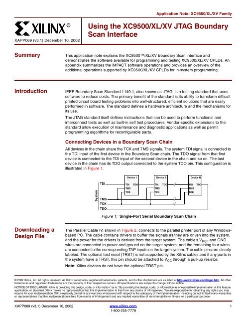
Application Note: <strong>XC9500</strong>/XL/XV Family<br />
XAPP069 (v3.1) December 10, 2002<br />
R<br />
<strong>Using</strong> <strong>the</strong> <strong>XC9500</strong>/XL/XV <strong>JTAG</strong> <strong>Boundary</strong><br />
<strong>Scan</strong> <strong>Interface</strong><br />
Summary<br />
This application note explains <strong>the</strong> <strong>XC9500</strong>/XL/XV <strong>Boundary</strong> <strong>Scan</strong> interface and<br />
demonstrates <strong>the</strong> software available for programming and testing <strong>XC9500</strong>/XL/XV CPLDs. An<br />
appendix summarizes <strong>the</strong> iMPACT software operations and provides an overview of <strong>the</strong><br />
additional operations supported by <strong>XC9500</strong>/XL/XV CPLDs for in-system programming.<br />
Introduction<br />
IEEE <strong>Boundary</strong> <strong>Scan</strong> Standard 1149.1, also known as <strong>JTAG</strong>, is a testing standard that uses<br />
software to reduce costs. The primary benefit of <strong>the</strong> standard is its ability to transform difficult<br />
printed circuit board testing problems into well-structured, efficient solutions that are easily<br />
performed in software. The standard defines a hardware architecture and <strong>the</strong> mechanisms for<br />
its use.<br />
The <strong>JTAG</strong> standard itself defines instructions that can be used to perform functional and<br />
interconnect tests as well as built-in self test procedures. Vendor-specific extensions to <strong>the</strong><br />
standard allow execution of maintenance and diagnostic applications as well as permit<br />
programming algorithms for reconfigurable parts.<br />
Connecting Devices in a <strong>Boundary</strong> <strong>Scan</strong> Chain<br />
All devices in <strong>the</strong> chain share <strong>the</strong> TCK and TMS signals. The system TDI signal is connected to<br />
<strong>the</strong> TDI input of <strong>the</strong> first device in <strong>the</strong> <strong>Boundary</strong> <strong>Scan</strong> chain. The TDO signal from that first<br />
device is connected to <strong>the</strong> TDI input of <strong>the</strong> second device in <strong>the</strong> chain and so on. The last<br />
device in <strong>the</strong> chain has its TDO output connected to <strong>the</strong> system TDO pin. This configuration is<br />
illustrated in Figure 1.<br />
Device 1<br />
Device 2<br />
Device N<br />
System<br />
TDI<br />
TMS<br />
TCK<br />
TDO<br />
TDI<br />
TMS<br />
TCK<br />
TDO<br />
TDI<br />
TMS<br />
TCK<br />
TDO<br />
TDI<br />
TMS<br />
TCK<br />
TDO<br />
Figure 1: Single-Port Serial <strong>Boundary</strong> <strong>Scan</strong> Chain<br />
Downloading a<br />
Design File<br />
The Parallel Cable IV, shown in Figure 2, connects to <strong>the</strong> parallel printer port of any Windowsbased<br />
PC. The cable contains drivers to buffer <strong>the</strong> signals as <strong>the</strong>y are driven into <strong>the</strong> system,<br />
and <strong>the</strong> power for <strong>the</strong> drivers is derived from <strong>the</strong> target system. The cable’s V REF and GND<br />
wires are connected to power and ground on <strong>the</strong> target system, and <strong>the</strong> remaining four wires<br />
are connected to <strong>the</strong> corresponding TAP inputs on <strong>the</strong> target system. The cable pins are clearly<br />
labeled. The optional test reset (TRST) is not supported by <strong>the</strong> Xilinx cables and if any parts in<br />
<strong>the</strong> system have a TRST, this pin should be attached to V CC through a pull-up resistor.<br />
Note: Xilinx devices do not have <strong>the</strong> optional TRST pin.<br />
© 2002 Xilinx, Inc. All rights reserved. All Xilinx trademarks, registered trademarks, patents, and fur<strong>the</strong>r disclaimers are as listed at http://www.xilinx.com/legal.htm. All o<strong>the</strong>r<br />
trademarks and registered trademarks are <strong>the</strong> property of <strong>the</strong>ir respective owners. All specifications are subject to change without notice.<br />
NOTICE OF DISCLAIMER: Xilinx is providing this design, code, or information "as is." By providing <strong>the</strong> design, code, or information as one possible implementation of this feature,<br />
application, or standard, Xilinx makes no representation that this implementation is free from any claims of infringement. You are responsible for obtaining any rights you may<br />
require for your implementation. Xilinx expressly disclaims any warranty whatsoever with respect to <strong>the</strong> adequacy of <strong>the</strong> implementation, including but not limited to any warranties<br />
or representations that this implementation is free from claims of infringement and any implied warranties of merchantability or fitness for a particular purpose.<br />
XAPP069 (v3.1) December 10, 2002 www.xilinx.com 1<br />
1-800-255-7778
R<br />
<strong>Using</strong> <strong>the</strong> <strong>XC9500</strong>/XL/XV <strong>JTAG</strong> <strong>Boundary</strong> <strong>Scan</strong> <strong>Interface</strong><br />
Figure 2: Parallel Cable IV<br />
x069_02_041202<br />
Figure 3 shows how <strong>the</strong> cable is connected to <strong>the</strong> printed circuit board for programming.<br />
Connect all six flying leads to <strong>the</strong> target board and observe <strong>the</strong> power sequencing<br />
recommendations.<br />
Memory<br />
FPGA<br />
ISP<br />
CPLD<br />
Pod<br />
FastFLASH<br />
PC or WS<br />
µP<br />
System<br />
Logic<br />
X5849<br />
Figure 3: Target PCB Connected for Program/Test<br />
Power<br />
Sequencing<br />
iMPACT<br />
Download<br />
Software<br />
Cable protection ensures that <strong>the</strong> parallel port cannot be damaged through normal cable<br />
operation. For increased safety, ensure that <strong>the</strong> PC is always powered up before <strong>the</strong> target<br />
system.<br />
When powering down, turn off <strong>the</strong> target system first, and <strong>the</strong>n turn off <strong>the</strong> host PC.<br />
Upon initiation of <strong>the</strong> iMPACT download software, <strong>the</strong> parallel port is queried to verify <strong>the</strong><br />
connection of <strong>the</strong> Parallel Cable IV. The cable must be attached and powered for proper<br />
verification. If an error message is returned, stating that <strong>the</strong> cable could not be found or<br />
indicating a cable o<strong>the</strong>r than <strong>the</strong> Parallel Cable IV was identified, check <strong>the</strong> cable connections<br />
to <strong>the</strong> PC parallel port. Figure 4 shows <strong>the</strong> iMPACT software user interface.<br />
<strong>Using</strong> <strong>the</strong> iMPACT Download Software<br />
See <strong>the</strong> iMPACT User Guide for detailed instructions. The following steps outline <strong>the</strong><br />
downloading procedure:<br />
1. Invoke <strong>the</strong> iMPACT software from <strong>the</strong> Project Navigator.<br />
2. Assign <strong>the</strong> files for each device in <strong>the</strong> chain ordered from system TDI to TDO (use JEDEC<br />
files for <strong>XC9500</strong>/XL/XV devices or BSDL files for o<strong>the</strong>r <strong>JTAG</strong>-compatible devices).<br />
3. Select <strong>the</strong> target <strong>XC9500</strong>/XL/XV devices to program.<br />
2 www.xilinx.com XAPP069 (v3.1) December 10, 2002<br />
1-800-255-7778
<strong>Using</strong> <strong>the</strong> <strong>XC9500</strong>/XL/XV <strong>JTAG</strong> <strong>Boundary</strong> <strong>Scan</strong> <strong>Interface</strong><br />
R<br />
4. Select <strong>the</strong> Operation → Program menu item with <strong>the</strong> Erase, before <strong>the</strong> programming and<br />
verify options. Detailed information regarding <strong>the</strong> downloading progress and any failure<br />
conditions will be displayed in <strong>the</strong> iMPACT log view.<br />
Figure 4: iMPACT User <strong>Interface</strong><br />
x069_04_041202<br />
Debugging a<br />
<strong>Boundary</strong> <strong>Scan</strong><br />
Chain<br />
If you are unable to establish communications with <strong>the</strong> <strong>Boundary</strong> <strong>Scan</strong> chain, <strong>the</strong> DEBUG<br />
CHAIN dialog can assist in <strong>the</strong> debugging of this problem. To access this dialog select File →<br />
Debug Chain ... You will <strong>the</strong>n see <strong>the</strong> dialog shown in Figure 5. You can control <strong>the</strong> values of<br />
<strong>the</strong> TMS, TDI, and <strong>the</strong> number of clock pulses as you step through <strong>the</strong> finite state machine of<br />
<strong>the</strong> test access port (TAP) controller. You will need to use an oscilloscope or logic probe to<br />
monitor TDO.<br />
Figure 5: <strong>Boundary</strong> <strong>Scan</strong> Chain Debug<br />
x069_05_052302<br />
A good fundamental check of your <strong>Boundary</strong> <strong>Scan</strong> chain is to execute a simple integrity test.<br />
The boundary scan integrity check sequences <strong>the</strong> TAP through a TRST sequence (TMS set to<br />
1, TCK pulsed 5 times) and <strong>the</strong>n transitions all devices to <strong>the</strong> RunTest/Idle state (TMS set to 0,<br />
TCK pulsed once). Then, all parts are run through a CAPTURE -IR sequence while TDI is set<br />
to 1 (so that “1”s will be shifted in). To do this set TMS to 1 and pulse TCK twice to enter <strong>the</strong><br />
Select-IR-<strong>Scan</strong> state. Then set TMS to 0 and pulse TCK twice to enter <strong>the</strong> Shift-IR state.<br />
XAPP069 (v3.1) December 10, 2002 www.xilinx.com 3<br />
1-800-255-7778
R<br />
<strong>Using</strong> <strong>the</strong> <strong>XC9500</strong>/XL/XV <strong>JTAG</strong> <strong>Boundary</strong> <strong>Scan</strong> <strong>Interface</strong><br />
If you look in <strong>the</strong> device BSDL files you will see <strong>the</strong> expected capture sequence defined in <strong>the</strong><br />
“INSTRUCTION_CAPTURE” field. This is <strong>the</strong> expected response shifted out at TDO in <strong>the</strong><br />
Shift-IR state. For all <strong>XC9500</strong>/XL/XV parts, this sequence is a “1” followed by seven zeros. You<br />
should <strong>the</strong>refore see <strong>the</strong> “1” on TDO after <strong>the</strong> falling edge of <strong>the</strong> fourth TCK pulse after <strong>the</strong><br />
TRST sequence. On <strong>the</strong> next TCK pulse TDO should return to zero. As you continue pulsing<br />
TCK in <strong>the</strong> Shift-IR state you will see <strong>the</strong> 1 to 0 transitions of <strong>the</strong> capture values. When all <strong>the</strong><br />
capture values have been shifted out you will see <strong>the</strong> sequence of logic “1”s input on TDI.<br />
See Appendix 1 for more details on <strong>the</strong> specific <strong>JTAG</strong> features supported.<br />
Interfacing to<br />
Third-Party<br />
<strong>Boundary</strong> <strong>Scan</strong><br />
Test Tools<br />
Appendix A<br />
<strong>JTAG</strong> Details<br />
BSDL files are required for interfacing to third-party <strong>Boundary</strong> <strong>Scan</strong> board test equipment<br />
(ATE), automatic test pattern generation software (ADAPT) and <strong>JTAG</strong>-based development and<br />
debugging systems. The BSDL files for all package variations of <strong>the</strong> available <strong>XC9500</strong>/XL/XV<br />
devices can be found in <strong>the</strong> Xilinx software “data” directory, where is ei<strong>the</strong>r<br />
<strong>XC9500</strong>, <strong>XC9500</strong>XL, or <strong>XC9500</strong>XV. The BSDL files re also available on <strong>the</strong> <strong>web</strong>:<br />
http://support.xilinx.com/support/sw_bsdl.htm<br />
In some circumstances silicon is updated and revised.<br />
Notes:<br />
1. The Xilinx iMPACT software is compatible with all version of <strong>the</strong> <strong>XC9500</strong>XL and <strong>XC9500</strong>XV families.<br />
However, <strong>the</strong> iMPACT software is compatible with only version 2 or later of <strong>the</strong> <strong>XC9500</strong> CPLD family.<br />
The Xilinx BSDL files follow a standard naming convention: device_package.bsd. For<br />
example, <strong>the</strong> BSDL file for <strong>the</strong> XC9536 in <strong>the</strong> PC44 package is xc9536_pc44.bsd and <strong>the</strong><br />
xc95144 in <strong>the</strong> TQ144 package is xc95144_tq144.bsd.<br />
The top level schematic of <strong>the</strong> test logic defined by IEEE Std. 1149.1 includes several key<br />
blocks as shown in Figure 6.<br />
I/O<br />
Pins<br />
<strong>Boundary</strong> <strong>Scan</strong> Cells<br />
Device<br />
Logic<br />
I/O<br />
Pins<br />
Test Register (10)<br />
Options PSTATUS (7)<br />
TDI Input<br />
Clocks/Shift Signals<br />
<strong>JTAG</strong> TAP<br />
Controller<br />
TMS TCK<br />
Configuration Register (27)<br />
Address (17) PDATA (8) Status (2)<br />
Identification Register (32)<br />
Version (4) Part No. (16) Manufacturer ID(11) (1)<br />
Bypass Register (1)<br />
USERCODE (32)<br />
Control/Enable Signals<br />
Instruction Decode<br />
OPCODE<br />
Instruction Register (8)<br />
Select<br />
TCK<br />
x069_06_041802<br />
Figure 6: <strong>JTAG</strong> Architecture<br />
4 www.xilinx.com XAPP069 (v3.1) December 10, 2002<br />
1-800-255-7778
<strong>Using</strong> <strong>the</strong> <strong>XC9500</strong>/XL/XV <strong>JTAG</strong> <strong>Boundary</strong> <strong>Scan</strong> <strong>Interface</strong><br />
R<br />
The TAP Controller<br />
The TAP controller responds to control sequences supplied through <strong>the</strong> test access port (TAP)<br />
and generates <strong>the</strong> clocks and control signals required by <strong>the</strong> o<strong>the</strong>r circuit blocks.<br />
The Instruction Register<br />
The instruction register is a shift register-based circuit and is serially loaded with instructions<br />
that select an operation to be performed.<br />
The Data Registers<br />
The data registers are a bank of shift registers. The stimuli required by an operation are serially<br />
loaded into <strong>the</strong> data registers, selected by <strong>the</strong> current instruction. Following execution of <strong>the</strong><br />
operation, results can be shifted out for examination.<br />
The <strong>JTAG</strong> Test Access Port<br />
The <strong>JTAG</strong> Test Access Port (TAP) has four pins that drive <strong>the</strong> circuit blocks and control specific<br />
operations. The TAP loads and unloads instructions and data. The four TAP pins are: TMS,<br />
TCK, TDI and TDO. The function of each TAP pin is:<br />
• TMS - Test Mode Select is <strong>the</strong> mode input signal to <strong>the</strong> TAP Controller. The TAP controller<br />
is a 16-state finite state machine (FSM) that controls <strong>the</strong> <strong>JTAG</strong> engine. At <strong>the</strong> rising edge<br />
of TCK, TMS determines <strong>the</strong> TAP controller state sequence. TMS has an internal pull-up<br />
resistor to provide a logic 1 to <strong>the</strong> system if TMS is not driven.<br />
• TCK - <strong>JTAG</strong> Test Clock sequences <strong>the</strong> TAP controller as well as all <strong>JTAG</strong> registers.<br />
• TDI -Test Data Input is <strong>the</strong> serial data input to all <strong>JTAG</strong> instruction and data registers. The<br />
TAP controller state and instruction register contents determine which register is fed by<br />
TDI for any operation. TDI has an internal pull-up resistor to provide a logic 1 to <strong>the</strong> system<br />
if TDI is not driven. TDI is loaded into <strong>the</strong> <strong>JTAG</strong> registers on TCK’s rising edge.<br />
• TDO - Test Data Out is <strong>the</strong> serial data output for all <strong>JTAG</strong> instruction and data registers.<br />
The TAP controller state and instruction register contents determine which register feeds<br />
TDO for a specific operation. Only one register (instruction or data) is connected between<br />
TDI and TDO for any <strong>JTAG</strong> operation. TDO changes state on TCK’s falling edge and is<br />
only active during <strong>the</strong> shifting of data through <strong>the</strong> device. TDO is in a 3-state condition at<br />
all o<strong>the</strong>r times.<br />
• TRST - [Optional] Asynchronous Test Reset for <strong>the</strong> <strong>JTAG</strong> TAP. The TRST pin is active-low.<br />
When reset, <strong>the</strong> TAP state machine is put into <strong>the</strong> Test-Logic-Reset state, and <strong>the</strong><br />
IDCODE instruction is loaded as <strong>the</strong> active instruction. Note that <strong>the</strong> BYPASS instruction<br />
is <strong>the</strong> default active instruction if <strong>the</strong> device does not support an IDCODE instruction.<br />
<strong>JTAG</strong> TAP Controller<br />
The TAP Controller is a 16-state FSM, that controls <strong>the</strong> loading of data into <strong>the</strong> various <strong>JTAG</strong><br />
registers. A state diagram of <strong>the</strong> TAP controller is shown in Figure 7.<br />
The state of TMS at <strong>the</strong> rising edge of TCK determines <strong>the</strong> sequence of state transitions. There<br />
are basically two state transition paths for sampling <strong>the</strong> signal at TDI: one for shifting<br />
information to <strong>the</strong> instruction register and one for shifting data into <strong>the</strong> data register.<br />
<strong>JTAG</strong> TAP Controller States<br />
Test-Logic-Reset<br />
This state is entered on device power-up when at least five TCK clocks occur with TMS held<br />
high. Entry into this state resets all <strong>JTAG</strong> logic so that it does not interfere with <strong>the</strong> normal<br />
component logic, and loads <strong>the</strong> IDCODE instruction into <strong>the</strong> instruction register.<br />
XAPP069 (v3.1) December 10, 2002 www.xilinx.com 5<br />
1-800-255-7778
R<br />
<strong>Using</strong> <strong>the</strong> <strong>XC9500</strong>/XL/XV <strong>JTAG</strong> <strong>Boundary</strong> <strong>Scan</strong> <strong>Interface</strong><br />
1<br />
Test-Logic-Reset<br />
0<br />
0<br />
Run-Test/Idle<br />
1<br />
Select-DR-<strong>Scan</strong><br />
1<br />
Select-IR-<strong>Scan</strong><br />
1<br />
0<br />
0<br />
1<br />
Capture-DR<br />
1<br />
Capture-IR<br />
0<br />
0<br />
Shift-DR<br />
0<br />
Shift-IR<br />
0<br />
1<br />
1<br />
Exit1-DR<br />
1<br />
Exit1-IR<br />
1<br />
0<br />
0<br />
Pause-DR<br />
0<br />
Pause-IR<br />
0<br />
1<br />
1<br />
0<br />
Exit2-DR<br />
0<br />
Exit2-IR<br />
1<br />
1<br />
Update-DR<br />
Update-IR<br />
1<br />
0<br />
1<br />
0<br />
x069_07_042202<br />
Figure 7: TAP Controller State Diagram<br />
Run-Test-Idle<br />
In this state, certain operations can occur depending on <strong>the</strong> current instruction. For <strong>the</strong><br />
<strong>XC9500</strong>/XL/XV family, “Run-Test-Idle” causes generation of <strong>the</strong> program, verify, erase, and<br />
POR (Power-On-Reset) pulses when <strong>the</strong> associated ISP instruction is active.<br />
Select-DR-<strong>Scan</strong><br />
This is a transitional state entered prior to performing a scan operation on a data register or in<br />
passing to <strong>the</strong> Select-IR-<strong>Scan</strong> state.<br />
Select-IR-<strong>Scan</strong><br />
This is a transitional state entered prior to performing a scan operation on <strong>the</strong> instruction<br />
register or in returning to <strong>the</strong> Test-Logic-Reset state.<br />
Capture-DR<br />
This state allows data to be loaded from parallel inputs into <strong>the</strong> data register selected by <strong>the</strong><br />
current instruction at <strong>the</strong> rising edge of TCK. If <strong>the</strong> selected data register has no parallel inputs,<br />
<strong>the</strong> register retains its state.<br />
Shift-DR<br />
In this state data is shifted by one stage in <strong>the</strong> currently selected register from TDI towards TDO<br />
by on each rising edge of TCK.<br />
Exit1-DR<br />
This is a transitional state allowing <strong>the</strong> option of passing to <strong>the</strong> Pause- DR state or transitioning<br />
directly to <strong>the</strong> Update-DR state.<br />
6 www.xilinx.com XAPP069 (v3.1) December 10, 2002<br />
1-800-255-7778
<strong>Using</strong> <strong>the</strong> <strong>XC9500</strong>/XL/XV <strong>JTAG</strong> <strong>Boundary</strong> <strong>Scan</strong> <strong>Interface</strong><br />
R<br />
Pause-DR<br />
This is a wait state that allows shifting of data to be temporarily halted.<br />
Exit2-DR<br />
This is a transitional state allowing <strong>the</strong> option of passing to <strong>the</strong> Update-DR state or returning to<br />
<strong>the</strong> Shift-DR state to continue accepting data.<br />
Update-DR<br />
In this state <strong>the</strong> data contained in <strong>the</strong> currently selected data register is loaded into a latched<br />
parallel output (for registers that have such a latch) on <strong>the</strong> falling edge of TCK after entering this<br />
state. The parallel latch prevents changes at <strong>the</strong> parallel register output from occurring during<br />
<strong>the</strong> shifting process.<br />
Capture-IR<br />
In this state data is loaded from parallel inputs into <strong>the</strong> instruction register on <strong>the</strong> rising edge of<br />
TCK. The least two significant bits of <strong>the</strong> parallel inputs must have <strong>the</strong> value 01, and <strong>the</strong><br />
remaining 6 bits are ei<strong>the</strong>r hard-coded or used for monitoring <strong>the</strong> security and data protect bits.<br />
Shift-IR<br />
In this state instruction register values are shifted one stage towards TDO on each rising TCK<br />
edge.<br />
Exit1-IR<br />
Exit1-IR is a transitional state allowing <strong>the</strong> option of transitioning to <strong>the</strong> Pause-IR state or <strong>the</strong><br />
Update-IR state.<br />
Pause-IR<br />
Pause-IR allows shifting of <strong>the</strong> instruction to be temporarily halted.<br />
Exit2-IR<br />
Exit2-IR is a transitional state allowing <strong>the</strong> option of passing to <strong>the</strong> Update-IR state or returning<br />
to <strong>the</strong> Shift-IR state to continue shifting in data.<br />
Update-IR<br />
In this state instruction register values are parallel latched on <strong>the</strong> falling edge of TCK. The<br />
parallel latch prevents changes at <strong>the</strong> parallel output of <strong>the</strong> instruction register from occurring<br />
during <strong>the</strong> shifting process.<br />
<strong>JTAG</strong><br />
Instructions<br />
Supported in<br />
<strong>XC9500</strong>/XL/XV<br />
Parts<br />
Mandatory <strong>Boundary</strong> <strong>Scan</strong> Instructions<br />
BYPASS<br />
The BYPASS instruction configures <strong>the</strong> device to bypass <strong>the</strong> scan registers and pass<br />
immediately to TDO.<br />
SAMPLE/PRELOAD<br />
The SAMPLE/PRELOAD instruction allows a snapshot of <strong>the</strong> normal operation of a component<br />
to be taken and examined. It also allows data values to be loaded onto <strong>the</strong> latched parallel<br />
outputs of <strong>the</strong> boundary scan shift register prior to <strong>the</strong> selection of o<strong>the</strong>r <strong>Boundary</strong> <strong>Scan</strong> test<br />
instructions.<br />
EXTEST<br />
The EXTEST instruction allows testing of off-chip circuitry and board level interconnections.<br />
XAPP069 (v3.1) December 10, 2002 www.xilinx.com 7<br />
1-800-255-7778
R<br />
<strong>Using</strong> <strong>the</strong> <strong>XC9500</strong>/XL/XV <strong>JTAG</strong> <strong>Boundary</strong> <strong>Scan</strong> <strong>Interface</strong><br />
<strong>XC9500</strong>/XL/XV Additional <strong>Boundary</strong> <strong>Scan</strong> Instructions<br />
INTEST<br />
The INTEST instruction allows testing of <strong>the</strong> on-chip system logic while <strong>the</strong> component is<br />
already on <strong>the</strong> board.<br />
HIGHZ<br />
HIGHZ permits automatic placement of all outputs on <strong>the</strong> <strong>XC9500</strong>/XL/XV part to high<br />
impedance (3-state) mode. This condition can be beneficial for board testing strategies.<br />
IDCODE<br />
The IDCODE instruction allows blind interrogation of <strong>the</strong> components assembled onto a printed<br />
circuit board to determine what components exist in a system.<br />
USERCODE<br />
The USERCODE instruction allows a user-programmable identification code to be shifted out<br />
for examination. This allows <strong>the</strong> programmed function of <strong>the</strong> component to be determined.<br />
<strong>XC9500</strong>/XL/XV Reconfiguration Instructions<br />
ISPEN<br />
ISPEN activates <strong>the</strong> <strong>XC9500</strong>/XL/XV device for In-System Programming.<br />
FPGM<br />
FPGM programs bits at specified addresses.<br />
FERASE<br />
FERASE erases a sectors of programming cells.<br />
FVFY<br />
FVFY verifies <strong>the</strong> programming at specified addresses.<br />
ISPEX<br />
ISPEX transfers <strong>the</strong> <strong>XC9500</strong>/XL/XV memory cell contents to internal low power configuration<br />
latches.<br />
FPGMI<br />
FPGMI programs bits at an internally generated address.<br />
FVFYI<br />
FVFYI verifies <strong>the</strong> programming at an internally generated address.<br />
FBULK<br />
FBULK erases several sectors of programming cells.<br />
Device Operations<br />
The programming information is extracted from <strong>the</strong> JEDEC file generated by <strong>the</strong> fitter software.<br />
The JEDEC file name is defaulted to design_name.jed.<br />
Device operation options available to users are:<br />
Erase, Program, Verify<br />
Download contents of <strong>the</strong> JEDEC file to <strong>the</strong> device programming registers. Erase <strong>the</strong> device,<br />
configure it, and read back <strong>the</strong> contents of device programming registers and compare <strong>the</strong>m to<br />
<strong>the</strong> JEDEC file. Report any differences to <strong>the</strong> user.<br />
8 www.xilinx.com XAPP069 (v3.1) December 10, 2002<br />
1-800-255-7778
<strong>Using</strong> <strong>the</strong> <strong>XC9500</strong>/XL/XV <strong>JTAG</strong> <strong>Boundary</strong> <strong>Scan</strong> <strong>Interface</strong><br />
R<br />
Verify<br />
Read back contents of <strong>the</strong> device programming registers and compare <strong>the</strong>m with <strong>the</strong> JEDEC<br />
file.<br />
Erase<br />
Clear <strong>the</strong> device configuration information.<br />
Functional Test<br />
Apply user-specified functional vectors from <strong>the</strong> JEDEC file to <strong>the</strong> device using <strong>the</strong> <strong>JTAG</strong><br />
INTEST instruction, and compare <strong>the</strong> results obtained with expected values. Report any<br />
differences.<br />
Read Device ID<br />
Read and display <strong>the</strong> contents of <strong>the</strong> <strong>JTAG</strong> IDCODE register.<br />
Read User Signature<br />
The signature value is set by <strong>the</strong> user at programming time. It is valid only after programming.<br />
This function reads <strong>the</strong> contents of <strong>the</strong> <strong>JTAG</strong> USERCODE register and displays <strong>the</strong> result.<br />
Readback<br />
Extracts contents of device programming registers and creates a new JEDEC file with <strong>the</strong><br />
results.<br />
Checksum<br />
Extract <strong>the</strong> contents of device programming registers and calculate a checksum for comparison<br />
with <strong>the</strong> expected value<br />
BSDL<br />
Description<br />
Summary<br />
JEDEC<br />
Description<br />
Summary<br />
The <strong>Boundary</strong> <strong>Scan</strong> Description Language (BSDL) describes <strong>the</strong> boundary scan features of a<br />
component. The system looks for BSDL files along <strong>the</strong> Xilinx\data path and in <strong>the</strong> current<br />
working directory. A BSDL file must be specified for each non-<strong>XC9500</strong>/XL/XV device in <strong>the</strong><br />
<strong>JTAG</strong> chain.<br />
The name of <strong>the</strong> BSDL file is assumed to be device_name.bsd.<br />
The JEDEC file is an ASCII file containing <strong>the</strong> configuration information and optionally <strong>the</strong><br />
vectors that can be used to verify <strong>the</strong> functional behavior of <strong>the</strong> configured part. A JEDEC file<br />
must be specified for each <strong>XC9500</strong>/XL/XV device in <strong>the</strong> <strong>JTAG</strong> chain; one JEDEC file is<br />
generated for each <strong>XC9500</strong>/XL/XV device in <strong>the</strong> system by <strong>the</strong> fitter software.<br />
The name of <strong>the</strong> JEDEC file is assumed to be design_name.jed.<br />
References 1. IEEE Std. 1149.1a 1993 Standard Test Access Port and <strong>Boundary</strong> <strong>Scan</strong> Architecture. 1993<br />
2. The <strong>Boundary</strong> <strong>Scan</strong> Handbook, Ken Parker, Klewer Academic Publishers, 1992<br />
3. JEDEC Standard, Standard Data Transfer Format Between Data Preparation System and<br />
Programmable Logic Device Programmer JESD3-C, June 1994.<br />
4. IEEE Std. 1149.1b Supplement (B) to Standard Test Access Port & <strong>Boundary</strong> <strong>Scan</strong><br />
Architecture, IEEE Std. 1149.1 - 1990, 1994.<br />
5. <strong>Boundary</strong> <strong>Scan</strong> Test: A Practical Approach, Harry Bleeker et al., Kluwer Academic<br />
Publishers, 1993.<br />
XAPP069 (v3.1) December 10, 2002 www.xilinx.com 9<br />
1-800-255-7778
R<br />
<strong>Using</strong> <strong>the</strong> <strong>XC9500</strong>/XL/XV <strong>JTAG</strong> <strong>Boundary</strong> <strong>Scan</strong> <strong>Interface</strong><br />
Revision<br />
History<br />
The following table shows <strong>the</strong> revision history for this document.<br />
Date Version Revision<br />
02/01/98 2.0 Revised release.<br />
06/03/02 3.0 Revised release.<br />
12/10/02 3.1 Minor edit to family name in page header.<br />
10 www.xilinx.com XAPP069 (v3.1) December 10, 2002<br />
1-800-255-7778