Design and experiments for the waveguide to coaxial cable adapter ...
Design and experiments for the waveguide to coaxial cable adapter ...
Design and experiments for the waveguide to coaxial cable adapter ...

Create successful ePaper yourself
Turn your PDF publications into a flip-book with our unique Google optimized e-Paper software.
CPC(HEP & NP), 2011, 35(1): 79–82 Chinese Physics C Vol. 35, No. 1, Jan., 2011<br />
<strong>Design</strong> <strong>and</strong> <strong>experiments</strong> <strong>for</strong> <strong>the</strong> <strong>waveguide</strong> <strong>to</strong> <strong>coaxial</strong><br />
<strong>cable</strong> <strong>adapter</strong> of a cavity beam position moni<strong>to</strong>r<br />
LI Xiang() 1,2,3 ZHENG Shu-Xin() 1,2,3;1)<br />
1 Department of Engineering Physics, Tsinghua University, Beijing 100084, China<br />
2 Key Labora<strong>to</strong>ry of Particle & Radiation Imaging (Tsinghua University),<br />
Ministry of Education, Beijing 100084, China<br />
3 Key Labora<strong>to</strong>ry of High Energy Radiation Imaging Fundamental<br />
Science <strong>for</strong> National Defense, Beijing 100084, China<br />
Abstract: The <strong>waveguide</strong> <strong>to</strong> <strong>coaxial</strong> <strong>cable</strong> <strong>adapter</strong> is very important <strong>to</strong> <strong>the</strong> cavity beam position moni<strong>to</strong>r<br />
(CBPM) because it determines how much of <strong>the</strong> energy in <strong>the</strong> cavity could be coupled outside. In this paper,<br />
<strong>the</strong> <strong>waveguide</strong> <strong>to</strong> <strong>coaxial</strong> <strong>cable</strong> <strong>adapter</strong> of a CBPM is designed <strong>and</strong> <strong>experiments</strong> are conducted. The curve<br />
shapes of <strong>experiments</strong> <strong>and</strong> simulations are very similar <strong>and</strong> <strong>the</strong> difference in reflection is less than 0.1. This<br />
progress provides a reliable method <strong>for</strong> designing <strong>the</strong> <strong>adapter</strong>.<br />
Key words:<br />
CBPM, <strong>waveguide</strong> <strong>to</strong> <strong>coaxial</strong> <strong>cable</strong> <strong>adapter</strong>, physics design, coupling coefficient<br />
PACS: 29.27.Fh, 29.27.Eg DOI: 10.1088/1674-1137/35/1/016<br />
1 Introduction<br />
The cavity beam position moni<strong>to</strong>r (CBPM) is<br />
used <strong>for</strong> measuring an electron beam’s transverse position.<br />
In order <strong>to</strong> make <strong>the</strong> beam transport along <strong>the</strong><br />
axis of facilities, CBPMs are assembled on linacs, injec<strong>to</strong>rs,<br />
<strong>and</strong> undula<strong>to</strong>rs of free electron lasers (FELs).<br />
The CBPM measures <strong>the</strong> beam’s transverse position<br />
using <strong>the</strong> dipole mode excited by <strong>the</strong> passing beam,<br />
<strong>and</strong> <strong>the</strong> dipole mode field is designed <strong>to</strong> transmit outwards<br />
through two stages of coupling in most of <strong>the</strong><br />
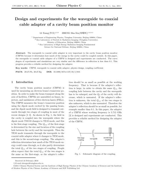
recent designs [1–3]. As shown in Fig. 1, <strong>the</strong> field in<br />
<strong>the</strong> cavity is coupled in<strong>to</strong> <strong>the</strong> <strong>waveguide</strong> where <strong>the</strong><br />
dipole mode TM110 changes <strong>to</strong> TE10 mode, <strong>and</strong> this<br />
is <strong>the</strong> first-stage coupling. The Q ext of <strong>the</strong> first-stage<br />
is determined by <strong>the</strong> size <strong>and</strong> location of <strong>the</strong> coupling<br />
hole between <strong>the</strong> cavity <strong>and</strong> <strong>the</strong> <strong>waveguide</strong>. Then <strong>the</strong><br />
TE10 mode transmits through <strong>the</strong> <strong>waveguide</strong> <strong>to</strong> <strong>the</strong><br />
<strong>coaxial</strong> <strong>cable</strong> <strong>adapter</strong> where it changes <strong>to</strong> TEM mode,<br />
<strong>and</strong> this is <strong>the</strong> second-stage coupling. The <strong>adapter</strong>’s<br />
reflection determines how much of <strong>the</strong> TE10 mode energy<br />
could come through, so it also partly determines<br />
<strong>the</strong> <strong>to</strong>tal Q ext of <strong>the</strong> two stages of coupling. People<br />
often expect that <strong>the</strong> <strong>to</strong>tal Q ext of <strong>the</strong> two stages is<br />
<strong>the</strong> same as <strong>the</strong> first-stage, so <strong>the</strong> <strong>adapter</strong>’s reflection<br />
should be as small as possible at <strong>the</strong> working<br />
frequency. That is because if <strong>the</strong> <strong>adapter</strong>’s reflection<br />
is large, in order <strong>to</strong> obtain <strong>the</strong> same Q ext <strong>the</strong><br />
coupling hole between <strong>the</strong> cavity <strong>and</strong> <strong>the</strong> <strong>waveguide</strong><br />
has <strong>to</strong> be enlarged, <strong>and</strong> <strong>the</strong> Q 0 of <strong>the</strong> cavity will decrease,<br />
which is unwanted. If <strong>the</strong> <strong>adapter</strong>’s reflection<br />
is unknown, <strong>the</strong> <strong>to</strong>tal Q ext of <strong>the</strong> two stages is<br />
also unknown, which is also unwanted. There<strong>for</strong>e <strong>the</strong><br />
<strong>adapter</strong>’s reflection should be as small as possible, <strong>for</strong><br />
example smaller than 0.1. In this paper, <strong>the</strong> <strong>adapter</strong><br />
of a CBPM whose working frequency is 5.712 GHz<br />
[3] is designed <strong>and</strong> <strong>experiments</strong> are conducted. This<br />
provides a reliable method <strong>for</strong> designing <strong>the</strong> <strong>adapter</strong><br />
of <strong>the</strong> CBPM.<br />
Fig. 1.<br />
Schematic diagram of <strong>the</strong> coupling.<br />
Received 23 February 2010<br />
1) E-mail: zhengsx@tsinghua.edu.cn<br />
©2011 Chinese Physical Society <strong>and</strong> <strong>the</strong> Institute of High Energy Physics of <strong>the</strong> Chinese Academy of Sciences <strong>and</strong> <strong>the</strong> Institute<br />
of Modern Physics of <strong>the</strong> Chinese Academy of Sciences <strong>and</strong> IOP Publishing Ltd
80 Chinese Physics C (HEP & NP) Vol. 35<br />
2 Physics design of <strong>the</strong> <strong>waveguide</strong> <strong>to</strong><br />
<strong>the</strong> <strong>coaxial</strong> <strong>cable</strong> <strong>adapter</strong><br />
2.1 Simulation modeling <strong>and</strong> physics design<br />
methods<br />
The reflection of <strong>the</strong> <strong>adapter</strong> is determined by two<br />
parameters: one is <strong>the</strong> distance between <strong>the</strong> probe of<br />
<strong>the</strong> SMA <strong>cable</strong> <strong>and</strong> <strong>the</strong> sealed end of <strong>the</strong> <strong>waveguide</strong>,<br />
which is defined as “ap”; <strong>the</strong> o<strong>the</strong>r one is <strong>the</strong> length<br />
of <strong>the</strong> probe, which is defined as “al”. The usual way<br />
<strong>to</strong> make <strong>the</strong> <strong>adapter</strong> is that “ap” is determined first<br />
<strong>and</strong> a hole <strong>to</strong> fixate <strong>the</strong> SMA feedthrough is drilled<br />
<strong>the</strong>re, <strong>and</strong> <strong>the</strong>n “al” is changed <strong>to</strong> search <strong>the</strong> smallest<br />
reflection. The simulation modeling <strong>and</strong> physics<br />
design methods we used are approximations <strong>to</strong> <strong>the</strong><br />
practical process.<br />
The 3D electromagnetic field simulation software<br />
MAFIA is used in physics design, <strong>and</strong> <strong>the</strong> simulation<br />
modeling is shown in Fig. 2. The <strong>waveguide</strong> is “BJ-<br />
84”, <strong>and</strong> it is made from oxygen-free copper. Its right<br />
end is sealed <strong>and</strong> <strong>the</strong>reby it short-circuits, <strong>and</strong> its left<br />
end is set as a nonreflecting port (Port-1). At <strong>the</strong><br />
upper side of <strong>the</strong> <strong>waveguide</strong> <strong>the</strong>re is an SMA <strong>coaxial</strong><br />
<strong>cable</strong>. The distance between its probe <strong>and</strong> <strong>the</strong><br />
right end of <strong>the</strong> <strong>waveguide</strong> is “ap”, <strong>and</strong> <strong>the</strong> length<br />
of <strong>the</strong> probe is “al”. The upper boundary of <strong>the</strong> <strong>cable</strong><br />
is also set as a nonreflecting port (Port-2). In<br />
simulation, <strong>the</strong> microwave power is fed from Port-2<br />
<strong>and</strong> <strong>the</strong> reflection fac<strong>to</strong>r S 22 is calculated. As mentioned<br />
above, <strong>the</strong> goal of physics design is <strong>to</strong> reduce<br />
S 22 at <strong>the</strong> working frequency as far as possible, so <strong>the</strong><br />
two parameters “ap” <strong>and</strong> “al” are adjusted <strong>to</strong> achieve<br />
that.<br />
The process of physics design is as follows [4].<br />
Firstly, <strong>the</strong> initial values of “ap” <strong>and</strong> “al” are set.<br />
Then one of <strong>the</strong>se two parameters (<strong>for</strong> example, “al”)<br />
is fixed, <strong>and</strong> <strong>the</strong> o<strong>the</strong>r one (“ap”) is swept. The<br />
curves of S 22 in <strong>the</strong> frequency range from 5.5 GHz<br />
<strong>to</strong> 6 GHz are calculated, <strong>and</strong> <strong>the</strong> “ap” corresponding<br />
<strong>to</strong> <strong>the</strong> smallest S 22 at 5.712 GHz is selected. This<br />
“ap” is set as <strong>the</strong> initial value of <strong>the</strong> second parameter<br />
sweep, in which “al” is swept. The curves of S 22 from<br />
5.5 GHz <strong>to</strong> 6 GHz are calculated again, <strong>and</strong> <strong>the</strong> best<br />
“al” is selected. Then this “al” is set as <strong>the</strong> initial<br />
value in <strong>the</strong> third parameter sweep. This process is<br />
repeated <strong>and</strong> <strong>the</strong> smallest S 22 at 5.712 GHz <strong>and</strong> <strong>the</strong><br />
corresponding “al” <strong>and</strong> “ap” are obtained.<br />
Theoretically, if “al” <strong>and</strong> “ap” change continuously,<br />
S 22 at a single frequency (<strong>for</strong> example,<br />
5.712 GHz) could decrease <strong>to</strong> zero. However, since<br />
<strong>the</strong> machining accuracy is not better than 0.1 mm,<br />
<strong>the</strong> sweep step of “al” <strong>and</strong> “ap” is set <strong>to</strong> 0.1 mm.<br />
Correspondingly, <strong>the</strong> goal of design is <strong>to</strong> reduce S 22<br />
at <strong>the</strong> working frequency as far as possible, <strong>and</strong> S 22<br />
should be lower than 0.1 in <strong>the</strong> neighboring frequency<br />
range (such as 100 MHz). There<strong>for</strong>e more than 99%<br />
of <strong>the</strong> microwave power is able <strong>to</strong> transmit through<br />
<strong>the</strong> <strong>adapter</strong> without reflection, so Q ext of <strong>the</strong> two<br />
stages of coupling will not deteriorate.<br />
Fig. 2.<br />
Schematic diagram of <strong>the</strong> simulation modeling.<br />
2.2 Results of <strong>the</strong> physics design<br />
Using <strong>the</strong> method discussed above, al=9 mm <strong>and</strong><br />
ap=10.8 mm are finally determined. S 22 at 5.712 GHz<br />
is 0.009, which is <strong>the</strong> minimum at this frequency.<br />
The curve of S 22 is shown in Fig. 4(a). The frequency<br />
range of S 22 < 0.1 around 5.712 GHz is about<br />
350 MHz, which achieves <strong>the</strong> goal of <strong>the</strong> design.<br />
3 Experimental results of <strong>the</strong> <strong>waveguide</strong><br />
<strong>to</strong> <strong>the</strong> <strong>coaxial</strong> <strong>cable</strong> <strong>adapter</strong><br />
3.1 Experimental set <strong>and</strong> method<br />
The experimental set is shown in Fig. 3(a), <strong>and</strong><br />
it consists of 3 parts. From left <strong>to</strong> right <strong>the</strong>re are a<br />
moving load with very small reflection, a <strong>waveguide</strong>,<br />
<strong>and</strong> a micrometer screw device. An SMA <strong>coaxial</strong> <strong>cable</strong><br />
pedestal, which is shown in Fig. 3(b), is assembled on<br />
<strong>the</strong> <strong>waveguide</strong>. The pedestal is connected with <strong>the</strong> <strong>cable</strong><br />
of a vec<strong>to</strong>r network analyzer (VNA), <strong>and</strong> because<br />
<strong>the</strong>y have <strong>the</strong> same impedance, <strong>the</strong>re is nearly no reflection<br />
at <strong>the</strong> port of <strong>the</strong> pedestal. There<strong>for</strong>e <strong>the</strong> port<br />
of <strong>the</strong> pedestal is equivalent <strong>to</strong> Port-2 in Fig. 2. The<br />
length of <strong>the</strong> probe is <strong>the</strong> key parameter “al” in simulation.<br />
In order <strong>to</strong> observe how S 22 changes with respect<br />
<strong>to</strong> “al”, several pedestals with different “al” are<br />
made <strong>and</strong> exchanged in <strong>experiments</strong>. The micrometer<br />
screw device pushes an oxygen-free copper block<br />
<strong>to</strong> move accurately in <strong>the</strong> <strong>waveguide</strong>, <strong>and</strong> <strong>the</strong> distance<br />
between <strong>the</strong> block <strong>and</strong> <strong>the</strong> probe is “ap”. The moving<br />
load is connected <strong>to</strong> <strong>the</strong> left port of <strong>the</strong> <strong>waveguide</strong>,
No. 1<br />
LI Xiang et al: <strong>Design</strong> <strong>and</strong> <strong>experiments</strong> <strong>for</strong> <strong>the</strong><br />
<strong>waveguide</strong> <strong>to</strong> <strong>coaxial</strong> <strong>cable</strong> <strong>adapter</strong> of a cavity beam position moni<strong>to</strong>r 81<br />
<strong>and</strong> because its reflection is very small, <strong>the</strong> microwave<br />
power in <strong>the</strong> <strong>waveguide</strong> can transmit outwards from<br />
<strong>the</strong> left port of <strong>the</strong> <strong>waveguide</strong> nearly without reflection.<br />
There<strong>for</strong>e <strong>the</strong> left port of <strong>the</strong> <strong>waveguide</strong> is equivalent<br />
<strong>to</strong> Port-1 in Fig. 2. In <strong>experiments</strong>, one of <strong>the</strong><br />
SMA pedestals is assembled on <strong>the</strong> <strong>waveguide</strong>, <strong>and</strong><br />
“ap” is controlled by <strong>the</strong> micrometer screw device.<br />
The moving load method [5] is used <strong>to</strong> measure S 22<br />
at 5.712 GHz under different “al” <strong>and</strong> “ap”, <strong>and</strong> <strong>the</strong><br />
experimental results are compared with those of <strong>the</strong><br />
simulation.<br />
Fig. 3. Pictures of <strong>the</strong> experimental set (a) <strong>and</strong><br />
SMA pedestals (b).<br />
3.2 Experimental results with respect <strong>to</strong><br />
“ap”<br />
According <strong>to</strong> <strong>the</strong> simulation results, at first <strong>the</strong><br />
SMA pedestal whose “al” is 9 mm is assembled on<br />
<strong>the</strong> <strong>waveguide</strong> <strong>and</strong> “ap” is set <strong>to</strong> 10.8 mm. The<br />
curve of S 22 from 5.5 GHz <strong>to</strong> 6 GHz is measured<br />
<strong>and</strong> compared with <strong>the</strong> simulation, which is shown<br />
in Fig. 4(a). The experimental result of S 22 reaches<br />
its minimum of 0.076 at <strong>the</strong> frequency of 5.67 GHz,<br />
<strong>and</strong> S 22 at 5.712 GHz is 0.09. The experimental st<strong>and</strong>ard<br />
deviation (SD) is approximately 0.01. The simulation<br />
result of S 22 reaches its minimum of 0.008 at<br />
5.71 GHz, <strong>and</strong> S 22 at 5.712 GHz is 0.009. In <strong>the</strong> frequency<br />
range around <strong>the</strong> minimum of S 22 , both of<br />
<strong>the</strong> two curves rise, <strong>and</strong> <strong>the</strong> slopes are close <strong>to</strong> each<br />
o<strong>the</strong>r in <strong>the</strong> higher frequency range. However, in <strong>the</strong><br />
lower frequency range <strong>the</strong> shapes of <strong>the</strong> curves are<br />
different. Because <strong>the</strong> experimental set is imperfect<br />
<strong>and</strong> is somewhat different from <strong>the</strong> simulation modeling,<br />
<strong>the</strong> difference of S 22 , which is about 0.1, seems<br />
reasonable.<br />
As mentioned above, when making <strong>the</strong> practical<br />
<strong>adapter</strong> of <strong>the</strong> CBPM, <strong>the</strong> distance between <strong>the</strong><br />
SMA feedthrough <strong>and</strong> <strong>the</strong> sealed end of <strong>the</strong> <strong>waveguide</strong><br />
(“ap”) will be determined first, <strong>and</strong> <strong>the</strong>n <strong>the</strong> hole<br />
<strong>to</strong> fixate <strong>the</strong> feedthrough will be drilled <strong>the</strong>re. Since<br />
it is difficult <strong>to</strong> repair <strong>the</strong> hole on <strong>the</strong> <strong>waveguide</strong>, people<br />
expect <strong>to</strong> predict <strong>the</strong> position of <strong>the</strong> feedthrough<br />
accurately according <strong>to</strong> <strong>the</strong> results of <strong>the</strong> physics design.<br />
There<strong>for</strong>e, besides <strong>the</strong> curve of S 22 from 5.5 GHz<br />
<strong>to</strong> 6 GHz, how <strong>the</strong> S 22 at 5.712 GHz changes with<br />
respect <strong>to</strong> “ap” is even more important. Fig. 4(b)<br />
shows <strong>the</strong> experimental <strong>and</strong> simulation results of S 22<br />
at 5.712 GHz when al=9 mm <strong>and</strong> ap=9.2–12.2 mm,<br />
<strong>and</strong> each point is measured by moving load method.<br />
It can be seen that <strong>the</strong> experimental result of S 22<br />
at 5.712 GHz reaches its minimum 0.08 when “ap” is<br />
10.4 mm. The experimental SD is less than 0.01. The<br />
simulation result reaches its minimum 0.009 when<br />
“ap” is 10.8 mm, <strong>and</strong> <strong>the</strong> difference between <strong>the</strong> experiment<br />
<strong>and</strong> simulation is less than 0.1. There<strong>for</strong>e<br />
people could find <strong>the</strong> best “ap” quite accurately by<br />
simulation.<br />
Although <strong>the</strong> approximation between <strong>experiments</strong><br />
<strong>and</strong> simulations has been demonstrated, people still<br />
need <strong>to</strong> consider <strong>the</strong> difference brought by error in<br />
practice. Fig. 4(c) shows <strong>the</strong> simulation result of <strong>the</strong><br />
minima of S 22 at 5.712 GHz <strong>for</strong> each “ap”, <strong>and</strong> from<br />
this curve people could predict <strong>the</strong> change of S 22 while<br />
“ap” has some error, or in o<strong>the</strong>r words how <strong>the</strong> error<br />
will affect S 22 . For example, if <strong>the</strong> error is 0.4 mm,<br />
which makes “ap” change from 10.8 mm <strong>to</strong> 10.4 mm,<br />
Fig. 4. Experimental <strong>and</strong> simulation results<br />
with respect <strong>to</strong> “ap”.
82 Chinese Physics C (HEP & NP) Vol. 35<br />
people know from <strong>the</strong> curve that <strong>the</strong> minimum of S 22<br />
will change from 0.009 <strong>to</strong> 0.02, which increases by<br />
0.01. And because <strong>the</strong> shapes of <strong>the</strong> experimental<br />
<strong>and</strong> simulation curves are very similar, people could<br />
predict that <strong>the</strong> measured minimum of S 22 will increase<br />
by about 0.01 in practice.<br />
3.3 Experimental results with respect <strong>to</strong> “al”<br />
After determining “ap”, people often adjust “al”<br />
<strong>to</strong> search <strong>the</strong> minimum of S 22 at 5.712 GHz, so how<br />
<strong>the</strong> S 22 at 5.712 GHz changes with respect <strong>to</strong> “al” is<br />
also very important. According <strong>to</strong> <strong>the</strong> experimental<br />
results shown in Fig. 4(b), “ap” is fixed <strong>to</strong> 10.4 mm,<br />
<strong>and</strong> <strong>the</strong> SMA pedestals whose “al” is different from<br />
9 mm are assembled <strong>to</strong> <strong>the</strong> <strong>waveguide</strong> in turn, <strong>and</strong><br />
<strong>the</strong> results of <strong>experiments</strong> <strong>and</strong> simulations are shown<br />
in Fig. 5. The SD of <strong>the</strong> experimental results is still<br />
approximately 0.01. It can be seen that <strong>the</strong> experimental<br />
results are a bit larger than simulation, but<br />
<strong>the</strong> difference between <strong>the</strong>m is less than 0.1, which<br />
means <strong>the</strong>y agree well with each o<strong>the</strong>r. According <strong>to</strong><br />
<strong>the</strong> fitting curves, ap=10.4 mm <strong>and</strong> al=9 mm is <strong>the</strong><br />
best choice in practice.<br />
Fig. 5. Experimental <strong>and</strong> simulation results<br />
with respect <strong>to</strong> “al”.<br />
4 Conclusions<br />
In this paper, <strong>the</strong> physics design <strong>and</strong> <strong>experiments</strong><br />
of a <strong>waveguide</strong> <strong>to</strong> <strong>coaxial</strong> <strong>cable</strong> <strong>adapter</strong> are discussed.<br />
The curves of S 22 in <strong>the</strong> frequency range from 5.5 GHz<br />
<strong>to</strong> 6 GHz, <strong>and</strong> <strong>the</strong> results with respect <strong>to</strong> “ap” (or<br />
“al”), are shown. The curve shapes of <strong>experiments</strong><br />
<strong>and</strong> simulations are very close <strong>and</strong> <strong>the</strong> difference in<br />
reflection is less than 0.1. There<strong>for</strong>e a reliable method<br />
of physics design <strong>for</strong> <strong>the</strong> <strong>adapter</strong> is provided.<br />
References<br />
1 Yoichi Inoue, Hi<strong>to</strong>shi Hayano, Yosuke Honda et al. Physical<br />
Review Special Topics -Accelera<strong>to</strong>rs <strong>and</strong> Beams, 2008,<br />
11: 062801<br />
2 Sean Wals<strong>to</strong>n, Stewart Boogert, Carl Chung et al. Nuclear<br />
Instruments <strong>and</strong> Methods in Physics Research A, 2007,<br />
578: 1–22<br />
3 CHU Jian-Hua, TONG De-Chun, ZHAO Zhen-Tang. Chinese<br />
Physics C (HEP & NP), 2008, 32(5): 385<br />
4 Yosuke Honda. Waveguide <strong>to</strong> Coaxial Cable Adapter <strong>for</strong> IP-<br />
BPM. http://acfahep.kek.jp/subg/ir/nanoBPM/library/<br />
honda.report/ipbpm <strong>adapter</strong> 0.050929.pdf<br />
5 YAO Chong-Guo. Electrical Linear Accelera<strong>to</strong>r. Beijing:<br />
Science Press, 1986. 572–587 (in Chinese)