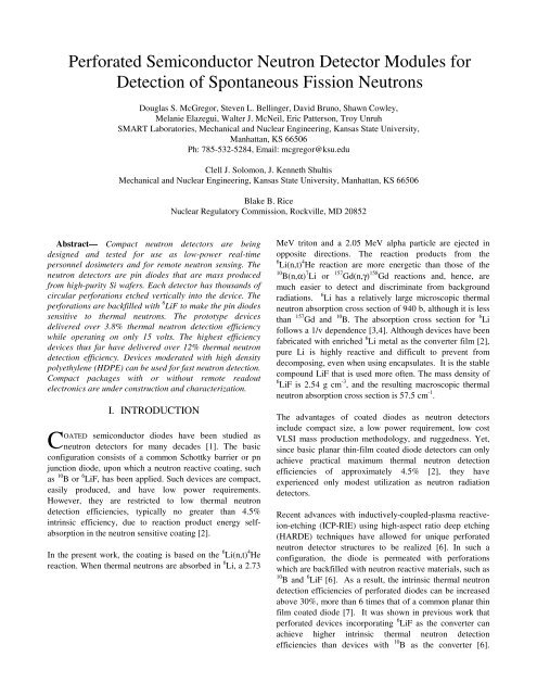
Perforated Semiconductor Neutron Detector Modules for Detection of
Perforated Semiconductor Neutron Detector Modules for Detection of
Perforated Semiconductor Neutron Detector Modules for Detection of

Create successful ePaper yourself
Turn your PDF publications into a flip-book with our unique Google optimized e-Paper software.
<strong>Per<strong>for</strong>ated</strong> <strong>Semiconductor</strong> <strong>Neutron</strong> <strong>Detector</strong> <strong>Modules</strong> <strong>for</strong><br />
<strong>Detection</strong> <strong>of</strong> Spontaneous Fission <strong>Neutron</strong>s<br />
Douglas S. McGregor, Steven L. Bellinger, David Bruno, Shawn Cowley,<br />
Melanie Elazegui, Walter J. McNeil, Eric Patterson, Troy Unruh<br />
SMART Laboratories, Mechanical and Nuclear Engineering, Kansas State University,<br />
Manhattan, KS 66506<br />
Ph: 785-532-5284, Email: mcgregor@ksu.edu<br />
Clell J. Solomon, J. Kenneth Shultis<br />
Mechanical and Nuclear Engineering, Kansas State University, Manhattan, KS 66506<br />
Blake B. Rice<br />
Nuclear Regulatory Commission, Rockville, MD 20852<br />
Abstract— Compact neutron detectors are being<br />
designed and tested <strong>for</strong> use as low-power real-time<br />
personnel dosimeters and <strong>for</strong> remote neutron sensing. The<br />
neutron detectors are pin diodes that are mass produced<br />
from high-purity Si wafers. Each detector has thousands <strong>of</strong><br />
circular per<strong>for</strong>ations etched vertically into the device. The<br />
per<strong>for</strong>ations are backfilled with 6 LiF to make the pin diodes<br />
sensitive to thermal neutrons. The prototype devices<br />
delivered over 3.8% thermal neutron detection efficiency<br />
while operating on only 15 volts. The highest efficiency<br />
devices thus far have delivered over 12% thermal neutron<br />
detection efficiency. Devices moderated with high density<br />
polyethylene (HDPE) can be used <strong>for</strong> fast neutron detection.<br />
Compact packages with or without remote readout<br />
electronics are under construction and characterization.<br />
C<br />
I. INTRODUCTION<br />
OATED semiconductor diodes have been studied as<br />
neutron detectors <strong>for</strong> many decades [1]. The basic<br />
configuration consists <strong>of</strong> a common Schottky barrier or pn<br />
junction diode, upon which a neutron reactive coating, such<br />
as 10 B or 6 LiF, has been applied. Such devices are compact,<br />
easily produced, and have low power requirements.<br />
However, they are restricted to low thermal neutron<br />
detection efficiencies, typically no greater than 4.5%<br />
intrinsic efficiency, due to reaction product energy selfabsorption<br />
in the neutron sensitive coating [2].<br />
In the present work, the coating is based on the 6 Li(n,t) 4 He<br />
reaction. When thermal neutrons are absorbed in 6 Li, a 2.73<br />
MeV triton and a 2.05 MeV alpha particle are ejected in<br />
opposite directions. The reaction products from the<br />
6 Li(n,t) 4 He reaction are more energetic than those <strong>of</strong> the<br />
10 B(n,α) 7 Li or 157 Gd(n,γ) 158 Gd reactions and, hence, are<br />
much easier to detect and discriminate from background<br />
radiations.<br />
6 Li has a relatively large microscopic thermal<br />
neutron absorption cross section <strong>of</strong> 940 b, although it is less<br />
than 157 Gd and 10 B. The absorption cross section <strong>for</strong> 6 Li<br />
follows a 1/v dependence [3,4]. Although devices have been<br />
fabricated with enriched 6 Li metal as the converter film [2],<br />
pure Li is highly reactive and difficult to prevent from<br />
decomposing, even when using encapsulates. It is the stable<br />
compound LiF that is used more <strong>of</strong>ten. The mass density <strong>of</strong><br />
6 LiF is 2.54 g cm -3 , and the resulting macroscopic thermal<br />
neutron absorption cross section is 57.5 cm -1 .<br />
The advantages <strong>of</strong> coated diodes as neutron detectors<br />
include compact size, a low power requirement, low cost<br />
VLSI mass production methodology, and ruggedness. Yet,<br />
since basic planar thin-film coated diode detectors can only<br />
achieve practical maximum thermal neutron detection<br />
efficiencies <strong>of</strong> approximately 4.5% [2], they have<br />
experienced only modest utilization as neutron radiation<br />
detectors.<br />
Recent advances with inductively-coupled-plasma reactiveion-etching<br />
(ICP-RIE) using high-aspect ratio deep etching<br />
(HARDE) techniques have allowed <strong>for</strong> unique per<strong>for</strong>ated<br />
neutron detector structures to be realized [6]. In such a<br />
configuration, the diode is permeated with per<strong>for</strong>ations<br />
which are backfilled with neutron reactive materials, such as<br />
10 B and 6 LiF [6]. As a result, the intrinsic thermal neutron<br />
detection efficiencies <strong>of</strong> per<strong>for</strong>ated diodes can be increased<br />
above 30%, more than 6 times that <strong>of</strong> a common planar thin<br />
film coated diode [7]. It was shown in previous work that<br />
per<strong>for</strong>ated devices incorporating 6 LiF as the converter can<br />
achieve higher intrinsic thermal neutron detection<br />
efficiencies than devices with 10 B as the converter [6].
Figure 1 - Per<strong>for</strong>ations are etched into the Si substrate with<br />
ICP-RIE. Shown are holes etched into Si, each 30 microns<br />
in diameter and 20 microns deep on a center-to-center pitch<br />
<strong>of</strong> 60 microns. A protective oxide has been grown in and<br />
around the perimeter <strong>of</strong> the holes.<br />
Figure 2 - 30 µm diameter and 100 µm deep per<strong>for</strong>ations in<br />
Si that have been completely backfilled with 6 LiF by using<br />
the low pressure condensation method.<br />
Figure 3 - The fabrication process developed to produce<br />
the per<strong>for</strong>ated detectors was designed <strong>for</strong> mass<br />
production.<br />
(Fig. 1). The hole pitch is 60 microns center-to-center. The<br />
active area <strong>of</strong> the detector is 25 mm 2 with the device<br />
diameter being 5.6 mm and die dimensions being 7 mm x 7<br />
mm. The per<strong>for</strong>ations in the first generation devices were<br />
backfilled by low pressure condensation deposition [8]. The<br />
wafer and 6 LiF powder are placed inside a vacuum furnace.<br />
The per<strong>for</strong>ated substrate is mounted to a cold plate inside<br />
the vacuum furnace. The 6 LiF powder is evaporated and<br />
transported with a carrier gas to the per<strong>for</strong>ated substrate<br />
where it condenses inside the miniature per<strong>for</strong>ations (Fig. 2).<br />
Presently, over 60 detectors can be produced per 3 inch<br />
diameter wafer, as shown in Fig. 3. The details <strong>of</strong> the<br />
detector processing steps can be found elsewhere [6,8].<br />
Basic Module Design<br />
First-generation per<strong>for</strong>ated detectors were coupled to a<br />
simple counting system with a low cost, low power, and a<br />
small transimpedance and gain amplifier combination. The<br />
amplifiers and a detection diode are located in a sealed 4 pin<br />
Hence, <strong>of</strong> the three main materials commonly used <strong>for</strong> thinfilm<br />
coated thermal neutron detectors, the following work<br />
concentrates only on devices constructed with 6 LiF as the<br />
converter material.<br />
<strong>Detector</strong> Dimensions<br />
II. DETECTOR DESIGN<br />
The per<strong>for</strong>ated detectors were produced as Si pin diodes.<br />
The diode fabrication processes were carried out on 3-inch<br />
diameter float zone, double-side polished, >5 kΩ-cm, n-type<br />
Si wafers approximately 325 µm thick. The devices have 30<br />
micron diameter holes that are typically between 20 to 100<br />
microns deep. The devices have an insulating coating inside<br />
the holes to reduce problems <strong>of</strong> excessive leakage current<br />
Figure 4 - Shown is a 6 LiF filled and coated per<strong>for</strong>ated<br />
detector, with a total active diameter <strong>of</strong> 5.6 mm, mounted<br />
alongside the preamplifier/amplifier circuit.
pin crystal carrier <strong>for</strong> noise isolation.<br />
Figure 5 - The per<strong>for</strong>ated detectors operate on minimal<br />
voltage. Shown are the internal parts to the module, with<br />
the detector, preamplifier/amplifier, power supply and<br />
digital display. The entire package is powered by 3 AAA<br />
batteries.<br />
(14 pin footprint) package widely used in the manufacture <strong>of</strong><br />
crystal oscillators (Fig. 4). The wire bonds between the<br />
diode and the transimpedance amplifier are also potted in an<br />
electronics grade epoxy to ensure stability. Once packaged,<br />
the detector plat<strong>for</strong>m is well shielded from external light,<br />
electrical noise, and humidity. The detector module (Fig. 5)<br />
supplies power <strong>for</strong> the amplifier and per<strong>for</strong>ated detector bias<br />
(nominally around 15 volts), and returns a positive polarity<br />
pulse output from neutron interactions between 70 and 130<br />
mV with a pulse width <strong>of</strong> approximately 4 µs (depending on<br />
the individual diode). The module requires an operating<br />
voltage between 2.7 to 5 volts at 150 µA. The module bias<br />
supply uses a charge pump circuit with an external<br />
adjustment potentiometer to supply between 10 and 20 volts<br />
<strong>of</strong> positive detector bias. It is based on a LT1615-1 DC/DC<br />
step up converter. The bias supply is also contained in a 4<br />
Pulse Width (µs)<br />
6.5<br />
6.0<br />
5.5<br />
5.0<br />
4.5<br />
4.0<br />
3.5<br />
90<br />
0 5 10 15 20<br />
Bias Voltage (volts)<br />
Pulse Width<br />
Pulse Height<br />
140<br />
130<br />
120<br />
110<br />
100<br />
Pulse Height (mV)<br />
Figure 6 - <strong>Detector</strong> output pulses as a function <strong>of</strong> applied<br />
bias. The pulse height reaches a maximum at 10 volts<br />
reverse bias, whereas the pulse width continues to decrease<br />
beyond 18 volts reverse bias.<br />
Pulses exiting the amplifier circuit are converted into a<br />
logic-level pulse <strong>for</strong> the counting circuits. An adjustable<br />
voltage level is set with a potentiometer and connected to<br />
the negative input <strong>of</strong> a low power comparator. The pulse is<br />
connected to the non-inverting input <strong>of</strong> the comparator with<br />
an r/c filter to remove a small dc <strong>of</strong>fset introduced by the<br />
amplification stage. This allows the device to “discriminate”<br />
pulse heights, as well as filter out spurious noise. The<br />
prototype arrangement operates on 3 AAA cell batteries (4.5<br />
volts), and uses a low power commercial counter to display<br />
neutron induced counts. The unit is constructed using<br />
surface mount components and techniques, and is housed in<br />
an aluminum box. Module testing was initially per<strong>for</strong>med<br />
with an 241 Am alpha-particle source. The aluminum housing<br />
has a hole drilled above the per<strong>for</strong>ated detector covered by<br />
an aluminized mylar window. The hole allows <strong>for</strong> the 5.5<br />
MeV alpha particles to enter the detector and produce<br />
pulses.<br />
The device modules were tested with an 241 Am alpha<br />
particle source <strong>for</strong> pulse width and pulse height as a function<br />
<strong>of</strong> bias voltage. The pulse widths, on average, leveled <strong>of</strong>f at<br />
approximately 3.7 µs beyond 15 volts bias. The pulse height<br />
leveled <strong>of</strong>f in magnitude at approximately 130 mV <strong>for</strong><br />
voltages exceeding 10 volts bias (Fig. 6). Since the depletion<br />
region need extend only beyond the holes to produce full<br />
charge collection, the voltage needed <strong>for</strong> optimum operation<br />
is actually less than needed <strong>for</strong> full depletion, observed to be<br />
35 volts from CV measurements.<br />
III. NEUTRON MEASUREMENTS<br />
The devices were tested in a tangential thermal beamport at<br />
the Kansas State University TRIGA Mark II Nuclear<br />
Reactor Facility. Each detector was tested in the same<br />
electronics box under identical conditions. The electronics<br />
box and detector were aligned in the beam port using an<br />
indexing holder. A thin film coated calibration detector,<br />
which had a coating <strong>of</strong> only 1400 angstroms <strong>of</strong> 95%<br />
enriched 6 LiF, was used to determine the average thermal<br />
flux at a reactor power <strong>of</strong> 225 kW, which yielded an average<br />
calibration flux unit <strong>of</strong> 1.1 n cm -2 s -1 W -1 ± 0.75%. Hence, at<br />
a reactor power <strong>of</strong> 200 W, the average slow flux at the<br />
indexed detector test location was 220 ± 1.65 n cm -2 s -1 as<br />
compared to the calibration detector.<br />
Figure 7 shows a calculated efficiency <strong>for</strong> a per<strong>for</strong>ated diode<br />
with 30 microns diameter 20 micron deep holes backfilled<br />
with 6 LiF. The spectral features and predicted efficiency<br />
were determined using the model described in the literature<br />
[7]. Distinct features include the 2.73 MeV single particle<br />
limit (from the triton) and the dual particle continuum,
Relative Counts Tallied<br />
10 5 2.73 MeV limit<br />
10 4<br />
10 3<br />
10 2<br />
10 1<br />
2.05 MeV limit<br />
Monte Carlo simulation<br />
Hole diameters = 30 microns<br />
Hole depths = 20 microns<br />
Hole pitch = 60 microns<br />
Cap thickness = 10 microns<br />
10 7 histories<br />
Maximum efficiency = 3.59%<br />
dual particle<br />
continuum<br />
0 1 2 3 4 5<br />
Energy Deposited (MeV)<br />
Recorded Counts<br />
10 5 2.73 MeV limit<br />
10 4<br />
10 3<br />
10 2<br />
10 1<br />
lower level<br />
discriminator<br />
limit<br />
0 1 2 3 4 5<br />
Scaled Energy (MeV)<br />
dual particle<br />
continuum<br />
Hole diameters = 30 microns<br />
Hole depths = 20 microns<br />
Hole pitch = 60 microns<br />
Cap thickness = 10 microns<br />
Efficiency = 3.8%<br />
pulse<br />
pileup<br />
Figure 7 - Calculated efficiency and spectral features <strong>for</strong><br />
a per<strong>for</strong>ated detector with 30 µm diameter 20 µm deep<br />
holes filled with 6 LiF.<br />
which will appear only if the per<strong>for</strong>ated device is<br />
functioning properly. By comparison, Fig. 8 shows a<br />
spectrum <strong>for</strong> a per<strong>for</strong>ated device with 30 micron diameter<br />
and 20 micron deep holes backfilled with 6 LiF. The<br />
measured thermal neutron detection efficiency was 3.8%,<br />
which compares well to the modeled result. Further, the 2.73<br />
Figure 8 - Measured efficiency and spectral features <strong>for</strong> a<br />
per<strong>for</strong>ated detector with 30 µm diameter 20 µm deep<br />
holes filled with 6 LiF.<br />
MeV single particle limit and the dual particle continuum<br />
are clearly present. Devices with holes 100 microns deep<br />
have yielded efficiencies above 12.5%.<br />
It is anticipated that the neutron detectors can be used <strong>for</strong><br />
fast neutron detection <strong>for</strong> remote sensing. In such a case, the<br />
modules can be packaged in high density polyethylene<br />
(HDPE) to scatter fast neutrons down to slow energies<br />
where the per<strong>for</strong>ated detectors have higher detection<br />
efficiency. A device <strong>of</strong> this sort can be stationed in locations<br />
capable <strong>of</strong> accumulating counts from a fast neutron source<br />
over a long period <strong>of</strong> time.<br />
Figure 9 shows a prototype per<strong>for</strong>ated neutron detector<br />
plat<strong>for</strong>m inserted between two HDPE disks, each being 2<br />
inches in diameter and two inches thick. The entire device is<br />
approximately the same size <strong>of</strong> a common 12 oz beverage<br />
can. The preamplifier, amplifier and charge pump are<br />
installed in the base <strong>of</strong> the HDPE moderator. Figure 10<br />
shows the response to fast neutrons from a 252 Cf source at<br />
distances ranging from 0.5 m to 2 m. The detector in the<br />
package was a low thermal neutron detection efficiency<br />
(2%) per<strong>for</strong>ated diode. There is a noticeable difference in<br />
the count rates as a function <strong>of</strong> HDPE cylinder orientation<br />
<strong>for</strong> detector to source distances less than 2 m. Higher count<br />
rates were observed with the HDPE cylinder oriented<br />
perpendicular to the neutron source as opposed to parallel.<br />
IV. REMOTE CAPABILITY<br />
Figure 9 - <strong>Per<strong>for</strong>ated</strong> detectors with miniature<br />
preamplifiers packaged in high density polyethylene<br />
(HDPE).<br />
The detector packages are being outfitted with commercial<br />
radio transmitter technology <strong>for</strong> remote applications. The<br />
wireless detector network is constructed <strong>of</strong> two major<br />
pieces. The first and most important piece is the detector<br />
board. The second piece is the wireless communications<br />
module.
8000<br />
7000<br />
Perpendicular<br />
Parallel<br />
Counts per Hour<br />
6000<br />
5000<br />
4000<br />
3000<br />
2000<br />
1000<br />
0<br />
60 80 100 120 140 160 180 200<br />
Distance from Source(cm)<br />
Figure 10 - Count rate <strong>of</strong> a 2% efficient per<strong>for</strong>ated<br />
semiconductor neutron detector packaged in high density<br />
polyethylene (HDPE) as a function <strong>of</strong> distance from a<br />
252 Cf source.<br />
The remote detector board combines three basic components<br />
needed to detect a neutron, as with the basic module, those<br />
being signal generation, bias supply, and digital converter.<br />
The same detector plat<strong>for</strong>m as shown in Fig. 4 is used. The<br />
bias supply is a simple adjustable capacitor charge pump. It<br />
is also contained within a crystal oscillator package, but it<br />
requires an external inductor to reduce power supply noise.<br />
After a neutron is detected, the pulse is passed through a<br />
high pass filter to remove any dc <strong>of</strong>fsets. Then the pulse is<br />
converted to a digital signal using a simple comparator<br />
circuit. The resulting digital pulse is connected to an<br />
interrupt line on the wireless module via a 51 pin connector<br />
on the underside <strong>of</strong> the detector board.<br />
The wireless module chosen <strong>for</strong> this prototype is<br />
manufactured by Crossbow, named a MICAz. This module<br />
con<strong>for</strong>ms to the new IEEE 802.15.4 ZigBee standard <strong>for</strong> low<br />
power wireless sensor networks, and operates in the 2.4<br />
GHz band. Some attractive features <strong>of</strong> ZigBee networks are<br />
low power requirements, large network sizes, and small<br />
processing and memory requirements. A full discussion <strong>of</strong><br />
the ZigBee protocol can be found elsewhere [9].<br />
One <strong>of</strong> the more attractive features <strong>of</strong> the ZigBee protocol is<br />
the mesh network. Any module or “mote” can act as a router<br />
or base station. As long as any individual mote is within<br />
range <strong>of</strong> another mote, messages can be chained back to the<br />
base station. According to the datasheet <strong>for</strong> the MICAz<br />
series <strong>of</strong> motes [10], the outdoor range is 75 – 100 m, and<br />
the indoor range is from 20 – 30 m, assuming a ½ wave<br />
dipole antenna and line <strong>of</strong> sight (<strong>for</strong> outdoor range). The<br />
lower frequency (900, 430 and 315MHz) MICA2 modules<br />
extend outdoor range to around 300 m. The combined<br />
detector board and remote transmitter is shown in Fig. 11.<br />
Figure 11 – <strong>Detector</strong> board, with the detector package<br />
and charge pump, mounted atop the remote transmitter<br />
module and battery package.<br />
Another attraction <strong>of</strong> the MICAz mote is the built in<br />
Atmega128 processor. The processor allows pulse counting<br />
from each detector, in which the counts are transmitted to a<br />
base computer via the mesh network. The Atmega128<br />
processor also has a built in A/D converter <strong>for</strong> future<br />
applications. The simple s<strong>of</strong>tware <strong>for</strong> the detector system<br />
utilizes an interrupt vector <strong>for</strong> the external interrupt pin to a<br />
subroutine which increments a counter. The mote sends the<br />
accumulated count back to the base station in regular<br />
intervals. If a large number <strong>of</strong> events are counted be<strong>for</strong>e the<br />
timed communication interval, the mote will report back to<br />
the base.<br />
V. CONCLUSIONS<br />
Si-based per<strong>for</strong>ated diode detectors have been fabricated<br />
and demonstrated in compact low-power packages. The<br />
shallow hole device yielded 3.8% thermal neutron detection<br />
efficiency. Future generation devices will be constructed<br />
from diodes with much deeper per<strong>for</strong>ations and a tighter<br />
per<strong>for</strong>ation matrix. Both changes will increase the intrinsic<br />
thermal neutron detection efficiency, with calculations and<br />
models indicating that efficiencies above 30% can be<br />
reached [7].<br />
We plan on extending our existing plat<strong>for</strong>m to include three<br />
detectors – one fast neutron, one thermal neutron, and a<br />
gamma ray detector (most likely CZT). The two neutron<br />
detectors are simple to interface to the processor since they<br />
only produce pulses. The gamma ray detector also provides<br />
pulses, but the pulse height in<strong>for</strong>mation will need to be<br />
stored as well. We can accomplish this by using a sample<br />
and hold circuit along with a discriminator circuit like those<br />
used in the neutron detectors. Once a pulse is detected, the<br />
sample and hold circuit will capture the peak voltage and the<br />
microprocessor will convert the peak into a number. The
number will be used as an index to an array that will be<br />
incremented each time a pulse <strong>of</strong> that specific height is<br />
detected.<br />
VI. ACKNOWLEDGEMENTS<br />
This work was supported under DTRA contract DTRA-01-<br />
03-C-0051, National Science Foundation IMR-MIP grant<br />
No. 0412208, and US Department <strong>of</strong> Energy NEER Grant<br />
DE-FG07-04ID14599.<br />
VII. REFERENCES<br />
[1] <strong>Neutron</strong> <strong>Detector</strong>s, International Atomic Energy<br />
Agency, Bibliographical Series, No. 18, Vienna, 1966.<br />
[2] D.S. McGregor, M.D. Hammig, H.K. Gersch, Y-H.<br />
Yang, and R.T. Klann, “Design Considerations <strong>for</strong><br />
Thin Film Coated <strong>Semiconductor</strong> Thermal <strong>Neutron</strong><br />
<strong>Detector</strong>s, Part I: Basics Regarding Alpha Particle<br />
Emitting <strong>Neutron</strong> Reactive Films,” Nuclear Instruments<br />
and Methods A500, 272-308, 2003.<br />
[3] D.I. Garber, R.R. Kinsey, BNL 325: <strong>Neutron</strong> Cross<br />
Sections, 3rd ed., Vol. 2, Curves, Brookhaven National<br />
Laboratory, Upton, 1976.<br />
[4] V. McLane, C.L. Dun<strong>for</strong>d, P.F. Rose, in: <strong>Neutron</strong><br />
Cross Sections, Vol.2, Academic Press, San Diego,<br />
1988.<br />
[5] D.S. McGregor, R.T. Klann, H.K. Gersch, E. Ariesanti,<br />
J.D. Sanders, and B. Van Der Elzen, “New Surface<br />
Morphology <strong>for</strong> Low Stress Thin-Film-Coated Thermal-<br />
<strong>Neutron</strong> <strong>Detector</strong>s,” IEEE Trans. Nuclear Science 49,<br />
1999-2004, 2002.<br />
[6] D.S. McGregor, S. Bellinger, D. Bruno, W. Dunn, W.J.<br />
McNeil, E. Patterson, B.B. Rice, J.K. Shultis,<br />
“<strong>Per<strong>for</strong>ated</strong> Diode <strong>Neutron</strong> <strong>Detector</strong> <strong>Modules</strong><br />
Fabricated from High-Purity Silicon,” Radiation<br />
Physics and Chemistry, 2007, in press.<br />
[7] J.K. Shultis and D.S. McGregor, “Efficiencies <strong>of</strong><br />
Coated and <strong>Per<strong>for</strong>ated</strong> <strong>Semiconductor</strong> <strong>Neutron</strong><br />
<strong>Detector</strong>s,” IEEE Trans. Nuclear Science NS-53,<br />
1659-1665, 2006.<br />
[8] D.S. McGregor, S. Bellinger, W.J. McNeil, E.<br />
Patterson, B.B. Rice, J.K. Shultis, “Non-Streaming<br />
High-Efficiency <strong>Per<strong>for</strong>ated</strong> <strong>Semiconductor</strong> <strong>Neutron</strong><br />
<strong>Detector</strong>s, Methods <strong>of</strong> Making Same and Measuring<br />
Wand Utilizing Same, US patent pending, 2007.<br />
[9] www.zigbee.com, March, 2007.<br />
[10] www.xbow.com/Products/Product_pdf_files/Wireless_p<br />
df/MICAz_Datasheet.pdf, March, 2007.