wavefront ics2115.pdf - Free Pro Audio Schematics
wavefront ics2115.pdf - Free Pro Audio Schematics
wavefront ics2115.pdf - Free Pro Audio Schematics

Create successful ePaper yourself
Turn your PDF publications into a flip-book with our unique Google optimized e-Paper software.
Integrated<br />
Circuit<br />
Systems, Inc.<br />
ICS2115<br />
WaveFront Synthesizer<br />
General Description<br />
The WaveFront Synthesizer, ICS2115, is an audio synthesis<br />
chip which utilizes wavetable lookup to produce 16-bit, CD<br />
quality sound. The internal memory management unit allows<br />
both ROM, for standard samples, and low cost DRAM, for soft<br />
loadable samples, to be connected directly to the ICS2115. The<br />
WaveFront Synthesizer presents the audio output in 16-bit<br />
linear form for conversion by a low cost CD-type DAC.<br />
Features<br />
• Capable of addressing up to 32 MB of wavetable ROM<br />
and up to 16 MB of wavetable DRAM<br />
• Variable Polyphony Rates: 24 voices at 44.1 kHz through<br />
32 voices at 33.8 kHz<br />
• Uses 16 bit linear, 8 bit linear, and 8 bit u-Law wavetable<br />
data<br />
• Serial output for a CD player-type DAC<br />
• Capable of using either a 68EC000 (with the ICS2116) or<br />
an ISA-based host for software control<br />
• Part of a complete design package that includes software<br />
drivers for Windows and DOS<br />
Block Diagram<br />
Applications<br />
• ISA based sound cards<br />
• Wavetable synthesizer daughter cards<br />
• External sound modules that connect to a PC’s serial or<br />
parallel port<br />
• Any system requiring a self contained unit that provides<br />
high quality music synthesis of General MIDI sounds, in<br />
a low cost design<br />
RAMREQ*<br />
DD<br />
Wave Table<br />
Memory<br />
Interface<br />
ROMA<br />
MA<br />
ROMEN<br />
BYTE<br />
RAMACK<br />
RAS*<br />
CAS*<br />
WE*<br />
SD<br />
SA<br />
IOR*<br />
IOW*<br />
CS*<br />
CSMM*<br />
DACK*<br />
TC<br />
RESET*<br />
SBHE*<br />
Host<br />
Interface<br />
Synthesis<br />
Engine<br />
DAC<br />
Interface<br />
SERDATA<br />
LRCLK<br />
BCK<br />
WDCLK<br />
DRQ<br />
IOCH16*<br />
MMIRQ<br />
IRQ<br />
IOCHRDY<br />
XTLI<br />
CLOCK<br />
XTLO<br />
WaveFront is a trademark of Integrated Circuit Systems, Inc.<br />
ICS2115fullRevB072694
ICS2115<br />
Pin Configuration<br />
ICS2115<br />
84-Pin PLCC<br />
ICS2115<br />
100-Pin TQFP<br />
2
ICS2115<br />
Pin Descriptions<br />
PIN NUMBER PIN NAME TYPE DESCRIPTION<br />
6-10, 12-17 MA TPUP2 Wavetable Muxed Address Bus.<br />
69-77 ROMA O Wavetable ROM Address.<br />
1-3, 84 CAS O2 Wavetable DRAM Column Address Strobe.<br />
61-68 DD B Wavetable Data Bus.<br />
4 RAS O2 Wavetable DRAM Row Address Strobe.<br />
5 WE TPUP Wavetable DRAM Write Enable.<br />
78 ROMEN O Wavetable ROM Enable/Byte Enable.<br />
79 BYTE O Wavetable ROM Byte Mode.<br />
20 RAMREQ IPUP Wavetable DRAM cycle request.<br />
19 RAMACK O Wavetable DRAM cycle acknowledge.<br />
27-32, 34-39 SD B Host Interface Data Bus.<br />
40-41 SA I Host Interface Address Bus.<br />
44 IOR I Host Interface Read Strobe (Active Low).<br />
45 IOW I Host Interface Write Strobe (Active Low).<br />
42 SBHE IPUP Host Interface Sixteen Bit Hardware Enable.<br />
54 IOCS16 SINK Host Interface I/O Channel Sixteen Wide.<br />
47 CS I Host Interface Synthesizer Chip Enable.<br />
48 CSMM I Host Interface Chip Select for MIDI Interface Emulation.<br />
53 DRQ SOURCE Host Interface DMA Request.<br />
49 DACK I Host Interface DMA Acknowledge.<br />
50 TC I Host Interface DMA Terminal Count.<br />
52 IOCHRDY SINK Host Interface I/O Channel Ready.<br />
56 IRQ B2 Host Interface Synthesizer IRQ.<br />
55 MMIRQ SOURCE Host Interface MIDI IRQ.<br />
46 RESET IPUPS Hardware Reset (Active Low).<br />
57 SERDATA O Serial Data Output.<br />
58 LRCK O Left/Right Clock.<br />
59 WDCK O Word Clock.<br />
60 BCK O Bit Clock.<br />
81 XTLO O (special) Crystal or N/C.<br />
82 XTL1 I (special) Crystal or Clock Input.<br />
11, 51 VDD PWR Power for chip core.<br />
18, 83 VDDP PWR Power for pad ring.<br />
33, 80 VSS GND Ground for chip core.<br />
25, 26, 43 VSSP GND Ground for pad ring.<br />
3
ICS2115<br />
Pin Type Descriptions<br />
PIN<br />
TYPE<br />
INPUT<br />
TYPE DRIVE<br />
PULLUP<br />
R<br />
PULL-<br />
DOWN R<br />
NOTES<br />
I TTL none none none TTL Input.<br />
IPUP TTL none yes none TTL Input with pull-up.<br />
IPUPS SCHMIDT none yes none SCHMIDT Input with pull-up.<br />
O n/a standard none none Output.<br />
O2 n/a high none none High Drive Output (200pF max load).<br />
B TTL standard none none TTL Bi-directional.<br />
B2 SCHMIDT standard none yes Drive only with pull-up.<br />
TPUP n/a standard yes none Tristate with pull-up.<br />
TPUP2 n/a medium yes none Tristate (medium drive) with pull-up<br />
(125pF max load).<br />
SINK n/a standard yes none Drive low only with pull-up.<br />
SOURCE n/a standard none yes Drive high only with pull-down.<br />
PWR n/a n/a none none Power terminal.<br />
GND n/a n/a none none Ground terminal.<br />
Absolute Maximum Ratings<br />
Supply Voltage . . . . . . . . . . . . . . . . . . . . . . . . . . . . . . -0.5V to 7.0V<br />
Logic inputs . . . . . . . . . . . . . . . . . . . . . . . . . . . . . . . . -0.5V to VDD + 0.5V<br />
Ambient operating temp. . . . . . . . . . . . . . . . . . . . . . . 0°C to 70°C<br />
Storage temperature . . . . . . . . . . . . . . . . . . . . . . . . . . -65°C to 150°C<br />
Stresses above those listed under Absolute Maximum Ratings may cause permanent damage to the device. This is a stress rating<br />
only and functional operation of the device at these or any other conditions above those indicated in the operational sections of<br />
the specifications is not implied. Exposure to absolute maximum rating conditions for extended periods may affect product<br />
reliability.<br />
4
ICS2115<br />
DC Electrical Characteristics<br />
VCC = 5.0V ± 10%; GND = 0V; TA = 0°C to 70°C<br />
PARAMETER SYMBOL TEST CONDITIONS MIN TYP MAX UNITS<br />
Supply Voltage VDD 4.75 5.00 5.25 V<br />
TTL Input Voltage Low VIL -0.30 0.80 V<br />
TTL Input Voltage High VIH 2.20 VDD+0.30 V<br />
Schmidt Input Voltage Low VILS -0.30 1.50 V<br />
Schmidt Input Voltage High VIHS 3.00 VDD+0.30 V<br />
XTLI Input Voltage Low VILX -0.30 1.50 V<br />
XTLI Input Voltage High VIHX 3.50 VDD+0.30 V<br />
Output Low Current<br />
IOL VOL=0.4V 4.0 6.0 mA<br />
Standard Drive<br />
Output High Current<br />
IOH VOH=2.8V -6.0 -4.0 mA<br />
Standard Drive<br />
Output Low Current<br />
IOL2 VOH=0.4V 6.0 9.0 mA<br />
Medium Drive<br />
Output High Current<br />
IOH2 VOH=2.8V -9.0 -6.0 mA<br />
Medium Drive<br />
Output Low Current<br />
IOL3 VOH=0.4V 9.0 12.0 mA<br />
High Drive<br />
Output High Current<br />
IOH3 VOH=2.8V -12.0 -9.0 mA<br />
High Drive<br />
Input Leakage Current<br />
IIN VSS < VIN < VDD -1.0 1.0 uA<br />
Standard Inputs<br />
Pull-up Current IPUP VIN = VSS 15.0 30.0 50.0 uA<br />
Pull-down Current IPDN VIN = VDD 50.0 90.0 150.0 uA<br />
XTLI Input/<br />
CXTL 20.0 pF<br />
Output Capacitance<br />
Note: All pins have a maximum capacitive load of 50pF unless noted otherwise.<br />
5
ICS2115<br />
AC Electrical Characteristics<br />
Please reference the timing diagram titled Host Interface Timing, below.<br />
HOST INTERFACE AC TIMING PARAMETERS<br />
PARAMETER SYMBOL FROM TO MIN MAX UNITS<br />
Address setup to command tAS 3 1 10 - nS<br />
Chip select setup to command tCS 5 1 10 - nS<br />
Address hold from command tAH 2 4 10 - nS<br />
Chip select hold from command tCH 2 6 10 - nS<br />
Command width tCW 1 2 100 - ns<br />
Address valid to /IOCS16 delay tAID 3, 5 7 0 50 nS<br />
IOCS16 hold from address invalid tIH 4, 6 8 0 50 nS<br />
Write data setup tDS 14 2 50 - nS<br />
Write data hold tDHW 2 15 10 - nS<br />
Read data delay (ready access) tDD 1 12 0 60 nS<br />
Read data hold tDHR 2 13 0 20 nS<br />
DACK setup to command tDAS 16 1 20 - nS<br />
DACK hold after command tDAH 2 17 50 - nS<br />
TC setup to command tTS 18 2 25 - nS<br />
TC hold after command tTH 2 19 n/a - nS<br />
TC width tTW 18 19 20 - nS<br />
6
ICS2115<br />
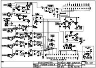
Timing Diagrams<br />
SA,SBHE*<br />
CS*,CSMM*<br />
3<br />
5<br />
4<br />
6<br />
IOR*,IOW*<br />
1<br />
2<br />
IOCS16*<br />
7<br />
8<br />
IOCHRDY<br />
9 10<br />
SD (Read)<br />
11<br />
12<br />
13<br />
SD (Write)<br />
14 15<br />
DACK* 16<br />
17<br />
TC<br />
18<br />
19<br />
Host Interface Timing<br />
1<br />
8<br />
16<br />
24<br />
BCK<br />
SERDATA<br />
15 Left (MSB)<br />
14 13<br />
12 11 10 9 8<br />
7 6 5 4 3 2 1 0<br />
WDCK<br />
LRCK<br />
24 32 40 48<br />
BCK<br />
SERDATA 1<br />
0<br />
15 Right (MSB)<br />
14 13<br />
12 11 10 9 8<br />
7 6 5 4 3 2<br />
1 0<br />
WDCK<br />
LRCK<br />
Notes:<br />
- BCK is XTLI frequency divided by four<br />
- ‘Extra’ cycles are appended as needed for the number of voices<br />
- BCK continues to run for all ‘extra’ cycles<br />
DAC Output Timing<br />
7
ICS2115<br />
XTLI/2<br />
RAS*<br />
CASn*<br />
CAS3*<br />
MA<br />
WE*<br />
DD (out)<br />
ROMA<br />
ROMEN<br />
BYTE<br />
(ONLY ONE ACTIVE)<br />
Refresh Synth 1 Synth 2<br />
8 Bit/u-Law Access of Wavetable ROM<br />
XTLI/2<br />
RAS*<br />
CASn*<br />
CAS3*<br />
MA<br />
WE*<br />
DD (out)<br />
ROMA<br />
ROMEN<br />
HIGH BYTE<br />
HIGH BYTE<br />
BYTE<br />
LOW BYTE<br />
LOW BYTE<br />
Refresh Synth 1 Synth 2<br />
16 Bit Access of Wavetable ROM<br />
8
ICS2115<br />
XTLI/2<br />
RAS*<br />
CASn*<br />
CAS3*<br />
MA<br />
WE<br />
(HIGH IMPEDANCE)<br />
(HIGH IMPEDANCE)<br />
DD (out)<br />
ROMA<br />
ROMEN<br />
BYTE<br />
Refresh Synth 1 Utility Synth 2<br />
8 BIt/u-Law Access of Wavetable DRAM<br />
SYNTH 16 Bit DRAM Access<br />
XTLI/2<br />
RAS*<br />
CASn*<br />
CAS3*<br />
MA<br />
MA0<br />
(HIGH IMPEDANCE)<br />
MA0<br />
WE<br />
(HIGH IMPEDANCE)<br />
DD (out)<br />
ROMA<br />
ROMEN<br />
BYTE<br />
Refresh Synth 1 Utility Synth 2<br />
16 Bit Access of Wavetable DRAM<br />
9
ICS2115<br />
Miscellaneous Pins<br />
VDD, VDDP<br />
These are the chip power supply pins. VDD pins power the core<br />
logic, while VDDP pins power the pad ring. This arrangement<br />
helps prevent switching spikes due to output transitions from<br />
disturbing the internal operation of the chip. These pins MUST<br />
be at the same potential externally.<br />
VSS, VSSP<br />
These are the chip ground pins. VSS pins ground the core logic,<br />
while VSSP pins ground the pad ring. This arrangement helps<br />
prevent switching spikes due to output transitions from disturbing<br />
the internal operation of the chip. These pins MUST be at<br />
the same potential externally.<br />
XTLI, XTLO<br />
These pins comprise a self-contained oscillator circuit for primary<br />
chip clock generation. No external components (other<br />
than the crystal itself) are required for fundamental mode<br />
operation. There is approximately 20pF of capacitance at each<br />
pin, and a DC bias feedback between the pins for startup and<br />
biasing. The standard crystal frequency is 33.868800 MHz (for<br />
24 oscillators at 44.1 kHz or 32 oscillators at 33.8 kHz). Due<br />
to the expense of fundamental mode crystals of this frequency,<br />
the oscillator can be operated in 3rd overtone mode with the<br />
addition to the XTLO pin of a series network to ground of a<br />
1.0H inductor and a 0.001F capacitor. In this case, the crystal<br />
fundamental frequency will be 11.2896 MHz.<br />
When an external clock is supplied, XTLO should be left<br />
floating. XTLI should be connected to the clock source via a<br />
series capacitor (0.001uF is recommended). Duty factor is not<br />
critical, since the clock is internally divided by two.<br />
Host Interface<br />
The ICS2115 can interface with the ISA bus or directly with<br />
the ICS2116. For more information, refer to the WaveFront<br />
Application Notes. (Please reference the timing diagram titled<br />
Host Interface Timing, above.)<br />
CS<br />
This input pin selects read/write access to the internal indirect<br />
registers, as selected by SA. This signal must be stable<br />
before, during, and after IOR or IOW strobes.<br />
CSMM<br />
This input pin selects read/write access to the Media Master and<br />
MIDI interface emulation registers, as selected by SA.<br />
This signal must be stable before, during, and after IOR or IOW<br />
strobes.<br />
SA<br />
These address input pins select one of four direct mapped<br />
registers as determined by the CS and CSMM pins. These<br />
signals must be stable before, during, and after IOR or IOW<br />
strobes.<br />
SBHE<br />
This input pin determines the access width for even addresses,<br />
and is ignored for odd addresses. It should be connected directly<br />
to the ISA bus for a 16-bit card. For 8-bit cards, it should be<br />
tied high.<br />
IOCS16<br />
This output pin indicates to the host that the current address is<br />
accessible as a word-wide (sixteen bit) data entity. It is based<br />
on the current value of the indirect register address, SA,<br />
and CS selecting a word-wide internal register. Under these<br />
conditions, IOCS16 drives low; otherwise, it is a resistive high.<br />
This output pin is unused with systems that contain the<br />
ICS2116. IOCS16 requires an external pull-up of 3.3K.<br />
SD<br />
This is the bi-directional data bus used for all register data<br />
transfers.<br />
IOR<br />
This input pin is used to read registers when low. SA, CS,<br />
CSMM, and SBHE must be stable before, during, and after the<br />
active low pulse on IOR.<br />
IOW<br />
This input pin is used to write registers when low. SA,<br />
CS, CSMM, and SBHE must be stable before, during, and after<br />
the active low pulse on IOW. SD must be stable before,<br />
during, and after the trailing (rising) edge of /IOW.<br />
IOCHRDY<br />
This output pin is normally in a resistive pull-up state. During<br />
IOR or IOW low times, this pin can become active (drive low)<br />
to indicate to the host that the requested data transfer is not<br />
ready, and that IOR or IOW should be held (stretched) until<br />
ready is signaled by IOCHRDY deactivating (resistive high).<br />
IOCHRDY requires an external pull-up of 3.3K.<br />
10
ICS2115<br />
DACK<br />
This input, when low, identifies the current IO operation as a<br />
DMA acknowledge operation. The current IO operation will<br />
interact with the DMA control logic in the ICS2115 as programmed,<br />
and cause DRQ to be de-asserted. This input must<br />
be held before, during, and after the IO command signal (IOR<br />
or IOW low).<br />
TC<br />
This input (along with DACK being low) signals that the<br />
current DMA operation is the last transfer, and that the ICS2115<br />
should shutdown its DMA logic after the current transfer is<br />
complete.<br />
DRQ<br />
This output pin is normally in a resistive low state. When DMA<br />
operation has been programmed and the proper status exists,<br />
the DRQ pin will drive high to indicate that the ICS2115 is<br />
ready to accept a DMA data transfer. Upon receipt of a low on<br />
the DACK input, DRQ will return to the resistive low state.<br />
When the ICS2115 is ready to continue DMA transfers, DRQ<br />
will again be asserted. This sequence repeats until DMA is<br />
terminated by either TC or a register write. DRQ requires an<br />
external pull-down of 1K.<br />
MMIRQ<br />
This output is normally in a resistive low state. Whenever an<br />
active Media Master interrupt occurs, it will drive high. When<br />
the interrupt condition is cleared, the pin returns to a resistive<br />
low state. MMIRQ requires an external pull-down of 1K.<br />
IRQ<br />
This output is normally in a resistive low state. Whenever an<br />
active internal interrupt occurs, it will drive high. When the<br />
interrupt condition is cleared, the pin returns to a resistive low<br />
state. IRQ requires an external pull-down of 1K.<br />
RESET<br />
This input is the active low hardware reset for the ICS2115.<br />
DAC Output<br />
The ICS2115 is designed to directly interface with consumer<br />
CD player type digital to analog converters. The<br />
interface is a 48 clock, MSB first, left/right multiplexed<br />
data stream. Depending on the number of oscillators enabled,<br />
there will be additional idle clocks generated after<br />
the data is output. (Please reference the timing diagram<br />
titled DAC Output Timing, above.)<br />
Some DACs that may be used are:<br />
• Phillips TDA1545<br />
• NEC UDP6376<br />
BCK<br />
This output pin is the bit clock for the DAC. The frequency<br />
of BCK is the frequency of XTLI divided by four. It<br />
always runs, even when the system has not initialized<br />
itself. The other DAC interface signals change on the<br />
falling edge of BCK, and are stable on the rising edge of<br />
BCK.<br />
SERDATA<br />
This output is the accumulated data of all ICS2115 oscillators,<br />
presented as signed binary two’s complement data,<br />
MSB first. The internal 16 bit data is sign-extended to 24<br />
bits, and presented left then right.<br />
LRCK<br />
LRCK indicates the stereo channel of the data just shifted<br />
out. It will transition high to low after bit 0 of the left data<br />
has been output, and transition low to high after bit 0 of<br />
the right data has been output.<br />
WDCK<br />
WDCK indicates the framing of the data being shifted out.<br />
It will transition low to high between bits 12 and 11 of<br />
both the left and right data words. It transitions high to low<br />
after bit 0 of both the left and right data words.<br />
11
ICS2115<br />
Wavetable Memory Interface<br />
(Please reference the timing diagrams that show the wavetable<br />
memory access cycles, above.) The ICS2115 is designed to<br />
directly interface to the following memory components:<br />
• dynamic RAM meeting the following parameters:<br />
• 80nS access time<br />
• Fast Page mode operations<br />
• CAS-before-RAS auto-refresh<br />
• 256K (9 addresses) to 4M (11 addresses) by 1 or 4<br />
(configured as byte wide)<br />
SIMM’s with an access time better than 80ns can also be used.<br />
• ROM meeting the following parameters:<br />
• 150nS address access time<br />
• 70nS output enable access times<br />
• byte-wide output<br />
The ICS2122-001, ICS2124-001 and ICS2124-002 comprise<br />
the ICS 2 MB and 4 MB patch sets respectively. Users of the<br />
WaveFront chipset can either buy ROMs directly from ICS or<br />
purchase the mask and produce the wavetable ROMs independently.<br />
Pin descriptions follow.<br />
DD<br />
This bus is a bi-directional data bus for the wavetable data. It<br />
functions as an input under all operations except for DMA<br />
writes to DRAM. This bus connects directly to the data pins of<br />
all wavetable DRAM and ROM.<br />
MA<br />
This output bus drives addresses to both DRAM and ROM<br />
wavetable memory.<br />
CAS<br />
These outputs function as both CAS inputs to up to four banks<br />
of DRAM and as addresses to ROM. For a DRAM cycle, only<br />
one of these four outputs will toggle active (low) at a time. For<br />
a refresh cycle, they all toggle low to refresh all DRAM<br />
simultaneously.<br />
RAS<br />
This output connects to the RAS pin of all wavetable DRAM<br />
chips RAS is generated for all DRAM access and refresh<br />
cycles, and remains high for all ROM cycles so that the /CAS<br />
pins can be used as ROM addresses.<br />
WE<br />
This tristate output connects to the WE pin of all wavetable<br />
DRAM. It is normally in a driven (or resistive) high state. It<br />
toggles low only for DMA write cycles.<br />
ROMA<br />
This bus provides addresses for ROM based oscillators. During<br />
refresh and DRAM cycles, these pins are driven high. The<br />
MA and CAS multiplex to provide the other address<br />
bits for the wavetable ROM. The table below shows the<br />
exact relation.<br />
Wavetable ROM address<br />
A0<br />
A1<br />
A2<br />
A3<br />
A4<br />
A5<br />
A6<br />
A7<br />
A8<br />
A9<br />
A10<br />
A11<br />
A12<br />
A13<br />
A14<br />
A15<br />
A16<br />
A17<br />
A18<br />
A19<br />
A20<br />
A21<br />
A22<br />
A23<br />
ICS2115 Signal<br />
MA<br />
MA<br />
MA<br />
MA<br />
MA<br />
MA<br />
MA<br />
MA<br />
MA<br />
RA<br />
RA<br />
RA<br />
RA<br />
RA<br />
RA<br />
RA<br />
RA<br />
RA<br />
CAS<br />
MA<br />
MA<br />
CAS<br />
CAS<br />
CAS<br />
12
ICS2115<br />
BYTE<br />
BYTE functions as Low Byte OE for the low byte ROM of a<br />
16-bit ROM pair. When using the ICS2122-001, this connects<br />
to the output enable on the ROM. When using the 4 MB patch<br />
set, BYTE connects to the OE on the ICS2124-001.<br />
ROMEN<br />
ROMEN functions as High Byte OE for the high byte ROM of<br />
a 16-bit ROM pair. For systems using the ICS2122-001, this<br />
pin is unused. When using the 4 MB patch set, ROMEN<br />
connects to the OE on the ICS2124-002.<br />
RAMREQ<br />
This input pin is used to request an external memory cycle. Its<br />
function is unused in the present design. RAMREQ should be<br />
tied high.<br />
RAMACK<br />
This output pin provides acknowledgment of an external memory<br />
cycle. It is unused in the current design.<br />
MPU-401/6850 Emulation Registers<br />
These 4 registers will be mapped at an offset determined by the<br />
CSMM input. The WaveFront Synthesizer only decodes the<br />
least significant 2 address bits. For identification purposes, this<br />
document refers to these registers as Emulation Base + 0<br />
through Emulation Base + 3.<br />
MIDI Emulation Control/Status Register<br />
The MIDI Control Status register can be configured as<br />
either a 6850 compatible or an MPU-401 compatible<br />
UART. The WaveFront Operating System writes to the IndEmulMode<br />
Register to indicate the mode of emulation.<br />
6850 Mode Control (Emulation Base + 0) (Write Only)<br />
The host can access this MIDI control register by writing to this<br />
address. The control register is mapped as follows.<br />
Reset (11-reset, else soft)<br />
Soft<br />
Transmit Interrupt Control<br />
Receive Interrupt Enable<br />
MIDI (6850) Control Register<br />
1:0 - Reset - Resets the MIDI Port<br />
11 = Reset (Resets Receive Interrupt and Receive<br />
Interrupt Enable)<br />
00, 01 and 10 = No Reset<br />
4:2 - Soft - Software controlled functions<br />
6:5 - Transmit Buffer Empty Interrupt Control<br />
01 = Interrupts are enabled<br />
00, 10 and 11 = Interrupts disabled<br />
7: - Receive Buffer Full Interrupt Enable<br />
1 = Interrupts enabled<br />
0 = Interrupts disabled<br />
6850 Mode Status (Emulation Base + 0) (Read Only)<br />
The host can access this MIDI status register by reading this<br />
address. The status register is mapped as follows.<br />
0: - Receive Buffer Full<br />
1 = full<br />
0 = empty<br />
1: - Transmit Buffer Empty<br />
1 = empty<br />
0 = full<br />
6:2 - Soft<br />
7: - Interrupt Request<br />
1 = Interrupt pending<br />
0 = Interrupt not pending<br />
Receive Buffer Full (RBF)<br />
Transmit Buffer Empty (TBE)<br />
Soft<br />
Interrupt Request (IRQ)<br />
MIDI (6850) Status Register<br />
13
ICS2115<br />
MPU-401 Mode Control (Emulation Base + 1) (Write Only)<br />
The host can access this MIDI control register by writing to this<br />
address. The control register mapping is software dependent.<br />
Soft<br />
MIDI (MPU-401) Control Register<br />
7:0 - Soft - Software controlled functions<br />
MPU-401 Mode Status (Emulation Base + 1) (Read Only)<br />
The host can access this MIDI status register by reading this<br />
address. The status register is mapped as follows.<br />
5:0 - Soft<br />
6: - Transmit Buffer Full<br />
1 = full<br />
0 = empty<br />
7: - Receive Buffer Empty<br />
1 = empty<br />
0 = full<br />
Soft<br />
Transmit Buffer Full (TBF)<br />
Receive Buffer Empty (RBE)<br />
MIDI (MPU-401) Status Register<br />
MIDI Emulation Data Register<br />
This register is the MIDI data port for writing and reading<br />
MIDI data. The host can transfer MIDI data between<br />
itself and the WaveFront Operating System via<br />
this register.<br />
6850 Mode Data (Emulation Base + 1) (Read/Write)<br />
Eight bit data.<br />
MPU-401 Mode Data (Emulation Base + 0) (Read/Write)<br />
Eight Bit data<br />
Registers Emulation Base + 2 and<br />
Emulation Base + 3<br />
These registers are reserved when the ICS2115 is in the<br />
host configuration<br />
Synthesizer Registers<br />
In the ICS2115, the Synthesis and General Purpose registers<br />
are accessed indirectly via the Indirect I/O Registers. These 4<br />
registers will be mapped at an offset determined by the CS<br />
input. For identification, this document refers to these registers<br />
as Synthesizer Base + 0 through Synthesizer Base + 3.<br />
Synthesizer Base + 0 R IRQ/Status<br />
Synthesizer Base + 1 R/W Register Address<br />
Synthesizer Base + 2 R/W Data Low Byte/Word<br />
Synthesizer Base + 3 R/W Data High Byte/Byte<br />
Interrupt status (Synthesizer Base + 0) Read Only<br />
Timer Interrupt<br />
Oscillator Interrupt<br />
DMA Interrupt<br />
Emulation Interrupt<br />
Reserved<br />
Busy<br />
Interrupt<br />
Interrupt Status Register<br />
Note: Reading this Register does NOT clear any of the bits.<br />
0: - Timer Interrupt<br />
This indicates that one or both of the 2 internal<br />
WaveFront timers has expired.<br />
1: - Oscillator Interrupt<br />
When this interrupt occurs the WaveFront Operating<br />
Systems reads the Oscillator Interrupt Address register<br />
to determine the oscillator that needs servicing.<br />
2: - DMA Interrupt<br />
The DMA channel has completed a transfer.<br />
3: - Emulation Interrupt<br />
When this occurs it indicates that a read or write has<br />
occurred with one of the High Level Emulation Control<br />
or Data registers<br />
4: - Reserved<br />
5: - Reserved<br />
6: - Busy<br />
Status bit which indicates that the previous write operation<br />
to an internal register has not yet completed and<br />
thus a new write should not be initiated.<br />
7: - Interrupt<br />
This is the Operating System interrupt from the<br />
ICS2115.<br />
14
ICS2115<br />
Indirect Register Access<br />
There are two types of indirect registers in the chips; Synthesizer<br />
and General Purpose. Due to the timing restrictions on<br />
access to the internal indirect registers, access to the two types<br />
of registers are handled differently. In ICS2115, register addresses<br />
$00 through $3F are Synthesizer registers (for both read<br />
and write), and all others are for General Purpose use.<br />
General Purpose registers are immediately available for access.<br />
Synthesizer registers are internally buffered so that the chip<br />
hardware completes the data transfers at the required times.<br />
The WaveFront Operating System can read and write internal<br />
Synthesizer registers using 8 or 16 bit reads and writes. Access<br />
is accomplished via the 3 indirect registers:<br />
Indirect Address (Synthesizer Base + 1)<br />
This will contain the address of the internal Synthesizer<br />
register.<br />
Indirect Data Lo (Synthesizer Base + 2)<br />
Contains the Least significant 8 bits of the data to be<br />
written to or read from the internal Synthesizer register<br />
addressed by the Indirect Address register.<br />
Indirect Data Hi (Synthesizer Base + 3)<br />
Contains the Most significant 8 bits of the data to be<br />
written to or read from the internal Synthesizer register<br />
addressed by the Indirect Address register.<br />
15
ICS2115<br />
Register Map<br />
The following list includes all the internal registers of the ICS2115 chip and their associated “indirect” addresses. All registers<br />
can be read and written unless otherwise indicated.<br />
Synthesizer Register Definitions<br />
Indirect<br />
Address Rd/Wr Size Mnemonic Description<br />
00 R/W 8 OscConf Oscillator Configuration<br />
01 R/W 16 OscFC Wavesample Frequency (6 Integer, 9 Fraction)<br />
02 R/W 16 OscStrtH Wavesample Loop Start Address (16 Integer)<br />
03 R/W 8 OscStrtL Wavesample Loop Start Address (4 Integer, 4 Fraction)<br />
04 R/W 16 OscEndH Wavesample Loop End Address (16 Integer)<br />
05 R/W 8 OscEndL Wavesample Loop End Address (4 Integer, 4 Fraction)<br />
06 R/W 8 VIncr Volume Increment<br />
07 R/W 8 VStart Volume Start Value<br />
08 R/W 8 VEnd Volume End Value<br />
09 R/W 16 VolAcc Volume Accumulator<br />
0A R/W 16 OscAccH Wavesample Address (16 Integer)<br />
0B R/W 16 OscAccL Wavesample Address (4 Integer, 9 Fraction)<br />
0C R/W 8 OscPan Pan Value (Note - 10 Bits on 2210)<br />
0D R/W 8 VCtl Volume Envelope Control<br />
0E R/W 8 ActiveOsc Active Voices<br />
0F Rd 8 IRQV Interrupt Source/Oscillator<br />
10 R/W 8 OscCtl Oscillator Control<br />
11 R/W 8 OscSAddr Static Address Bits 27-20<br />
12 R/W 8 VMode Reserved (Write 0)<br />
13-3F - X RESERVED Do Not Access<br />
16
ICS2115<br />
General Purpose Register Definitions<br />
Indirect<br />
Address Rd/Wr Size Mnemonic Description<br />
40 Wr 8 Timer1 Timer Preset 1<br />
41 Wr 8 Timer2 Timer Preset 2<br />
42 Wr 8 Timer1PreS Prescaler 1<br />
43 R/W 8 Timer2PreS_S Prescaler 2 (wr) and Timer Status (Rd)<br />
44 Wr 8 DMAddrLo DMA Start Address Low [11:4]<br />
45 Wr 8 DMAddrMd DMA Start Address Medium [19:12]<br />
46 Wr 8 DMAddrHi/Data DMA Start Address high [21:20]<br />
47 R/W 8 DMACS DMA Control/Status<br />
48 Rd 8 AccMonS Accumulator Monitor Status<br />
49 Rd 16 AccMonData Accumulator Monitor Data<br />
4A R/W 8 DOCIntCS DOC Interrupt (Read) Int Enable (Write)<br />
4B Rd 8 IntOscAddr Address of interrupting Oscillator<br />
4C R/W 8 MemCfg_Rev Memory Config. (WR) & Chip Rev. # (Rd)<br />
4D R/W 8 SysCtrl System Control<br />
4E - X RESERVED Do Not Access<br />
4F R/W 8 OscNumber Oscillator Address being programmed<br />
50 R/W 8 IndMIDIData MIDI Data Register<br />
51 R/W 8 IndMIDICS MIDI Control/Status Register<br />
52 R/W 8 IndHostData Host Data Register<br />
53 R/W 8 IndHostCS Host Control/Status Register<br />
54 R/W 8 IndMIDIIntC MIDI Emulation interrupt Control<br />
55 R/W 8 IndHostIntC Host Emulation Interrupt Control<br />
56 R/W 8 IndIntStatus Host/MIDI Emulation Int. Status (Rd)<br />
57 R/W 8 IndEmulMode Emulation Mode<br />
58-7F - X RESERVED Do Not Access
ICS2115<br />
LEAD<br />
COUNT<br />
FRAME<br />
THICKNESS<br />
TF<br />
+/-.0003<br />
PKG.<br />
THICKNESS<br />
TP<br />
+/-.004<br />
PKG. WIDTH<br />
TOP<br />
WT<br />
+/-.004<br />
PKG. WIDTH<br />
BOTTOM<br />
WB<br />
+/-.066<br />
OVERALL<br />
PKG. WIDTH<br />
WO<br />
+/-.005<br />
CONTACT<br />
WIDTH<br />
WO<br />
+.010/-.030<br />
20L 0.010 0.152 0.350 0.323 0.390 0.320<br />
28L 0.010 0.152 0.450 0.423 0.490 0.420<br />
44L 0.010 0.152 0.650 0.623 0.690 0.620<br />
52L 0.010 0.152 0.750 0.723 0.790 0.720<br />
68L 0.008 0.150 0.950 0.923 0.990 0.920<br />
84L 0.008 0.150 1.160 1.123 1.190 1.120<br />
Ordering Information<br />
ICS2115V<br />
Example:<br />
ICS XXXX M<br />
Package Type<br />
V=PLCC<br />
Device Type (consists of 3 or 4 digit numbers)<br />
Prefix<br />
ICS, AV=Standard Device; GSP=Genlock Device<br />
18
ICS2115<br />
TQFP Package<br />
LEAD COUNT<br />
32L<br />
BODY THICKNESS 1.00 1.40<br />
FOOTPRINT (BODY+) 2.00<br />
DIMENSIONS<br />
TOLERANCE<br />
A MAX. 1.20 1.60<br />
A1<br />
0.05 MIN./0.10 MAX.<br />
A2 ±0.5 1.00 1.40<br />
D ±0.25 9.00<br />
D1 ±0.10 7.00<br />
E ±0.25 9.00<br />
E1 ±0.10 7.00<br />
L ±0.15/-0.10 0.60<br />
e BASIC 0.80 0.50<br />
b +0.05 0.35 0.22<br />
ccc MAX. 0.10 0.08<br />
ddd 0.20 MAX. 0.08 MAX.<br />
Ordering Information<br />
Example:<br />
ICS2115T<br />
ICS XXXX M<br />
Package Type<br />
T=TQFP<br />
Device Type (consists of 3 or 4 digit numbers)<br />
Prefix<br />
ICS, AV=Standard Device; GSP=Genlock Device<br />
19