
Create successful ePaper yourself
Turn your PDF publications into a flip-book with our unique Google optimized e-Paper software.
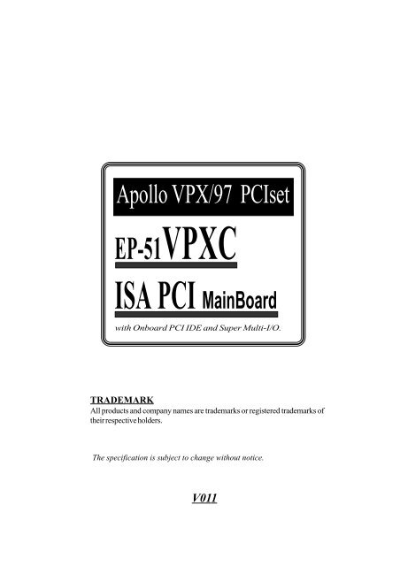
Apollo VPX/97 PCIset<br />
<strong>EP</strong>-<strong>51VPXC</strong><br />
ISA PCI MainBoard<br />
with Onboard PCI IDE and Super Multi-I/O.<br />
TRADEMARK<br />
All products and company names are trademarks or registered trademarks of<br />
their respective holders.<br />
The specification is subject to change without notice.<br />
V011
Package Checklist<br />
Please check your package which should include all items listed below.<br />
If you find any item damaged or any missing item, please contact your<br />
supplier.<br />
One motherboard<br />
One manual<br />
One IDE ribbon cable<br />
One floppy ribbon cable
Contents<br />
page<br />
Chapter 1 - Introduction......................................................1-1<br />
Chapter 2 - Hardware Design ............................................2-1<br />
2-1 Mainboard Layout........................................................... 2-1<br />
2-2 Connectors and Jumpers .................................................. 2-3<br />
2-3 System Memory Configuration ........................................ 2-5<br />
2-4 Integrated PCI Bridge ....................................................... 2-6<br />
Chapter 3 - Award BIOS Setup ..........................................3-1<br />
3-1 Standard CMOS Setup ..................................................... 3-2<br />
3-3 BIOS Features Setup ........................................................ 3-2<br />
3-3 Chipset Features Setup .................................................... 3-6<br />
3-4 Power Management Setup ............................................... 3-8<br />
3-5 PNP/PCI Configuration .................................................... 3-10<br />
3-6 Integrated Peripherals ....................................................... 3-12<br />
3-7 Load Setup Defaults ........................................................ 3-14<br />
3-8 Change Supervisor or User Password ............................. 3-15<br />
3-9 IDE HDD Auto Detection ................................................ 3-16<br />
3-10 HDD Low Level Format .................................................... 3-18<br />
3-11 Save & Exit Setup ............................................................. 3-18<br />
3-11 Exit Without Saving ......................................................... 3-18<br />
Chapter 4 - Onboard Technical Information ..................... 4-1<br />
4-1 I/O & Memory Map ......................................................... 4-1<br />
4-2 Time & DMA Channels Map ........................................... 4-2<br />
4-3 Interrupt Map ................................................................... 4-2<br />
4-4 RTC & CMOS RAM Map ................................................ 4-3<br />
Appendix A: Post Codes .......................................................... 4-4<br />
Appendix B: I/O Connector ..................................................... 4-8
NOTE :<br />
The "LOAD SETUP DEFAULTS" function loads the system default data directly from<br />
ROM and initializes the associated hardware properly. This function is necessary when<br />
you accept this mainboard, or the system CMOS data will corrupt.<br />
STANDARD CMOS SETUP<br />
BIOS FEATURES SETUP<br />
CHIPSET FEATURES SETUP<br />
POWER MANAGEMENT SETUP<br />
ROM PCI/ISA BIOS<br />
CMOSSETUPUTILITY<br />
AWARD SOFTWARE, INC.<br />
SUPERVISOR PASSWORD<br />
USER PASSWORD<br />
IDE HDD AUTO DETECTION<br />
HDD LOW LEVEL FORMAT<br />
PNP/PCI CONFIGURA<br />
Load SETUP Default (Y/N)? Y<br />
ETUP<br />
INTEGRATED PERIPH SAVING<br />
LOAD SETUP DEFAULTS<br />
ESC: QUIT :SELECT ITEM<br />
F10:Save & Exit Setup<br />
(Shift)F2 :Change Color<br />
Load Setup Defaults Except Standard COMS SETUP<br />
LOADSETUPDEFAULT
Specification<br />
Introduction 1-1<br />
Chapter 1<br />
Introduction<br />
This mainboard is a high performance system hardware based on Intel<br />
Pentium processor and is equipped with three PCI slots, two standard ISA<br />
slots, Super Multi-I/O controller and dual port PCI-IDE connectors for the<br />
future expansion. The hardware dimension is 243mm x 190mm micro ATX<br />
form factor with a four-layer-design technology.<br />
VIA Apollo VPX/97 PCIset chipset.<br />
R<br />
Intel Pentium Processor, AMD K5/K6 , Cyrix 6x86L/6x86MX & idt C6<br />
operating at 120 ~ 333 MHz and P55C with 321 ZIF socket 7 and<br />
scalability to accept faster Processors in the future.<br />
Supports up to 256 MegaBytes of DRAM (a minimum of 8 MB) on board (<br />
168-pin DIMM x 2). BIOS will autometically detect and configure FP/EDO<br />
and Synchronous DRAM.<br />
Supports 512KB Onboard Pipelined Burst (synchronous) L2 Cache.<br />
Supports two 16 bit ISA slots and three 32 bit PCI slots and provides two<br />
independent high performance PCI IDE interfaces capable of supporting<br />
PIO Mode 3/4 and Ultra-DMA33 devices. This mainboard supports four<br />
PCI Bus Masters and a jumperless PCI INT# control scheme which reduces<br />
configuration confusion when plugging in PCI I/O controller card(s).<br />
Supports ATAPI (e.g. CD-ROM) devices on both IDE interfaces.<br />
Supports 1 floppy port, 1 parallel port (<strong>EP</strong>P,ECP port), 2 serial ports (16550<br />
Fast UART compatible) and dual USB ports .<br />
Supports a PS/2 style mouse and keyboard connectors.<br />
Supports Award Plug & Play BIOS . The BIOS is stored in Flash <strong>EP</strong>ROM<br />
form. It provides better upgradeability for the system.<br />
Supports CPU Hardware sleep and SMM (System Management Mode).<br />
This mainboard utilizes Lithium battery which provides environmental<br />
protection and longer battery life.<br />
Supports an ATX power connector for a Remote On/Off, a Phone Ring<br />
Power On and Wake-up On LAN function.
Hardware Design 2-1<br />
Chapter 2<br />
Hardware design<br />
2-1 Mainboard Layout<br />
This mainboard is designed with VIA Apollo VPX/97 PCIset chipset which is<br />
R<br />
developed by VIA Corporation to fully support Pentium Processor PCI/ISA system.<br />
The chipset provides an integrated IDE controller with two high performance IDE<br />
interfaces for up to four IDE devices (hard devices, CD-ROM device, etc). The<br />
Winbond W83877TF Super I/O controller provides the standard PC I/O function:<br />
one floppy interface, two 16 Byte FIFO serial ports and one <strong>EP</strong>P/ECP capable parallel<br />
port. This mainboard layout is shown in the next page for user's reference. Care must<br />
be taken when inserting memory modules, CPUs or even plugging PCI card into<br />
associated slots to avoid damaging any circuits or sockets on board. A cooling fan is<br />
strongly recommended when installing Pentium/Pentium MMX/K5/K6/6x86L/<br />
6x86MX/C6 processor due to possible overheat.<br />
This mainboard supports a minimum of 8MB and a maximum of 256MB of System<br />
Memory while Onboard 512KB cache to increase system performance.<br />
This mainboard supports standard Fast Page, EDO (Extended Data Out or Hyper<br />
Page Mode) or synchronous DRAM. This mainboard provides two 168-pin<br />
DIMM sites for memory expansion. The sockets support 1M x 64(8MB), 2M x 64<br />
(16MB), 4M x 64(32MB), and 8M x 64(64MB) single-sided or double-sided memory<br />
modules. The memory timing requires 70 ns Fast page devices or 60 ns EDO DRAM.<br />
(DRAM Modules may be parity [x 36] or non-parity [x 32].<br />
This mainboard supports two Onboard PCI IDE connectors, and automatically<br />
detects IDE harddisk type by BIOS utility automatic.<br />
This mainboard supports Award Plug & Play BIOS for the ISA and PCI cards. The<br />
BIOS can be located in Flash <strong>EP</strong>ROM which can replace BIOS code easily if<br />
necessary.
12<br />
12<br />
12<br />
12<br />
12<br />
12<br />
12<br />
12<br />
12<br />
12<br />
12<br />
12<br />
12<br />
12<br />
2-2 <strong>EP</strong>-<strong>51VPXC</strong><br />
<strong>EP</strong>-<strong>51VPXC</strong> Layout<br />
12<br />
12<br />
MOUSE<br />
K/B<br />
COM2 COM1 USB PS/2<br />
PORT<br />
PRINTER PORT<br />
1<br />
1<br />
1<br />
1<br />
1<br />
1231<br />
1 123<br />
1<br />
1<br />
1<br />
1<br />
1<br />
ATX Power Conn.<br />
BANK1<br />
BANK0<br />
DIMM2<br />
DIMM1<br />
J4<br />
587VP<br />
64K64<br />
587VP<br />
SW1<br />
123456<br />
ON<br />
11<br />
12<br />
SOCKET 7<br />
JP2<br />
1<br />
2<br />
Winboand<br />
83877TF<br />
585VPX<br />
FDD CONN.<br />
Primary IDE<br />
Secondary IDE<br />
<<br />
BIOS<br />
J7<br />
PCI#1<br />
PCI#2<br />
PCI#3<br />
586B<br />
Power-ON<br />
<br />
1 5 + +<br />
IR CONN HD-LED TB-LED<br />
1 5<br />
RESET SPEAKER KEYLOCK<br />
Note : SW1 setting<br />
ON<br />
1 2 3 4 5 6<br />
Figure 2-1<br />
ON<br />
ON<br />
: Means ON : Means OFF
SW1 : CPU Selection<br />
*<br />
Hardware Design 2-3<br />
2-2 Connectors and Jumpers<br />
This section describes the connectors, jumpers and switch equipped in the<br />
mainboard. Please refer to Figure 2-1 for the location of each connector and jumper.<br />
1 2 3 4 5 6<br />
ON OFF<br />
OFF<br />
ON ON OFF<br />
OFF ON OFF<br />
OFF OFF OFF<br />
ON OFF ON<br />
ON ON ON<br />
OFF ON ON<br />
ON OFF<br />
OFF<br />
OFF OFF OFF<br />
OFF ON ON<br />
ON OFF ON<br />
ON OFF OFF<br />
OFF OFF<br />
OFF<br />
OFF ON ON<br />
ON OFF ON<br />
ON OFF<br />
OFF<br />
OFF OFF OFF<br />
OFF ON ON<br />
OFF OFF OFF<br />
idt C6<br />
Pentium MMX<br />
Bus Freqency<br />
x<br />
Cyrix & IBM<br />
AMD K5 / K6 Multiplier 6x86(L) / 6x86MX<br />
120MHz 60MHz x 2 6x86L-PR150<br />
133MHz 66MHz x 2 6x86/L/MX-PR166<br />
75MHz x 2 6x86/L/MX-PR200<br />
83MHz x 2<br />
150MHz 60MHz x 2.5 6x86MX-PR166<br />
166MHz 66MHz x 2.5 6x86MX-PR200<br />
188MHz 75MHz x 2.5 6x86MX-PR233<br />
83MHz x 2.5<br />
180MHz 60MHz x 3<br />
200MHz 66MHz x 3 6x86MX-PR233<br />
*<br />
225MHz 75MHz x 3 6x86MX-PR266<br />
233MHz 66MHz x 3.5 6x86MX-PR266<br />
*<br />
266MHz 66MHz x 4<br />
*<br />
300MHz 66MHz x 4.5<br />
333MHz 66MHz x 5<br />
*<br />
These settings are reserved for the future CPUs versions. When the future CPUs<br />
are ready and suitable for this mainboard, these settings will be correctly updated.<br />
JP2 : CPU Vcore voltage selection :<br />
11-12 : 3.5V for Pentium, AMD K5, Cyrix 6x86 and idt C6<br />
9-10 : 3.2V for AMD K6-PR2-233<br />
7-8 : 2.9V for AMD K6-PR2-166/200 and Cyrix 6x86MX<br />
5-6 : 2.8V for Pentium MMX and Cyrix 6x86L<br />
3-4 : 2.2V for AMD K6 3D CPUs<br />
1-2 : 2.1V Reserved
2-4 <strong>EP</strong>-<strong>51VPXC</strong><br />
J2<br />
5<br />
1<br />
KeyLock - Keyboard lock switch & Power LED connector.<br />
5. GND<br />
4. Key-Lock<br />
3. GND<br />
2. N/C<br />
1. Power LED(+)<br />
Speaker - connect to the system's speaker for beeping.<br />
4 4. VCC<br />
3. GND<br />
2. N/C<br />
1 1. Speaker<br />
Reset Switch - Closed to restart system.<br />
J3<br />
+<br />
5<br />
+<br />
Power-ON-Push the button to turn on the system.<br />
-Pressing less than 4 seconds to enter the suspend mode<br />
-Pressing more than 4 seconds to turn off the system<br />
Turbo LED indicator - LED ON when higher speed is selected.<br />
# There is no deturbo function so that the turbo LED is always ON.<br />
IDE LED indicator - LED ON when harddisks activate.<br />
IrDA/ASK IR CONNECTOR<br />
5. IRTX<br />
4. GND<br />
3. IRRX<br />
2. N/C<br />
1. VCC<br />
J4<br />
CPU FAN Connector<br />
J7<br />
WOL(Wake-up On Lan) Connector
12345<br />
12345<br />
123456789<br />
123456789<br />
12345678901234<br />
12345678901234<br />
Hardware Design 2-5<br />
2-3 System Memory Configuration<br />
This mainboard supports different type of settings for the system memory. The<br />
following figures and table provides all possible memory combinations.<br />
12<br />
12<br />
12<br />
12<br />
DIMM2<br />
><br />
12<br />
12<br />
DIMM1<br />
BANK 1<br />
BANK 0<br />
DIMM 1(BANK 0) DIMM 2(BANK 1) TOTAL MEMORY SIZE<br />
8MB<br />
16MB<br />
32MB x 1<br />
64MB<br />
128MB<br />
8MB<br />
16MB<br />
32MB x 1<br />
64MB<br />
128MB<br />
MAX.= 256MB<br />
NOTE 1 : The KEY ZONE of the DIMM socket is 3.3V / Unbuffered.<br />
DRAM chip<br />
LEFT KEY ZONE<br />
(Unbuffered DRAM)<br />
CENTER KEY ZONE<br />
(3.3V DRAM)
2-6 <strong>EP</strong>-<strong>51VPXC</strong><br />
2-4 Integrated PCI Bridge<br />
The <strong>EP</strong>-<strong>51VPXC</strong> utilizes VIA Apollo VPX/97 PCIset chipset to support Intel<br />
Pentium Processor PCI/ISA system. The VIA Apollo VPX/97 PCIset chipset<br />
consists of the 82C585VPX AT system controller (TSC), and one 82C586B PCI ISA/<br />
IDE Accelerator bridge chip. It provides an interface which translates CPU cycle into<br />
PCI bus cycle, and PCI burst read/write capability. In addition, it provides high<br />
performance PCI arbitor to support four PCI Masters, Rotating Priority Mechanism,<br />
and Hidden Arbitration Scheme Minimizes Arbitration Overhead.<br />
There are four interrupts in each PCI slot : INTA#, INTB#, INTC#, and INTD#. Since<br />
this mainboard adapts the PCI auto-configuration with the system BIOS Setup utility.<br />
When the system is turned on after adding a PCI add-in card, the BIOS automatically<br />
configure interrupts, DMA channels, I/O space, and other paramaters. You do not<br />
have to configure jumpers or worry about potential resource conflicts. Because PCI<br />
cards use the same interrupt resource as ISA cards, you must specify the interrupt<br />
used by ISA add-in cards in the BIOS Setup utility.<br />
However, if a "Legacy card" (such as plugging a paddle card and cable into an ISA<br />
slot) is plugged in the system, modification in the ROM SETUP UTILITY becomes<br />
necessary. First of all, you must enter PCI CONFIGURATION SETUP utility from<br />
the ROM SETUP UTILITY main menu to set "ISA" for the "PCI IDE IRQ MAP TO<br />
Secondly, you must enter the CHIPSET FEATURES SETUP UTILITY from the ROM<br />
SETUP UTILITY main menu and set "Disabled" for the "Onboard Primary PCI IDE<br />
and the Onboard Secondary PCI IDE. When you plug PCI/ISA IDE cards into the<br />
system, You should select "Disabled" for the Onboard Primary and Secondary PCI<br />
IDE from the CHIPSET FEATURES SETUP UTILITY too.<br />
You can set the system interrupt request (IRQ) on some "Legacy cards" which have<br />
on paddle card and cable. (refer to user's manual of the card) to a proper system IRQ<br />
level (In general, card's Primary is assigned to INTA and Secondary is assigned to<br />
INTB). If the card is plugged into slot 1(marked PCI#1), you cannot use second slot<br />
(marked PCI#2) because the Secondary INT signal takes INTB from the slot (refer to<br />
Page 3-12 for circuit diagram). The user then enters the PCI CONFIGURATION<br />
SETUP utility from the ROM SETUP UTILITY main menu and set "PCI-Slot 1" for<br />
the "PCI IDE IRQ MAP TO (This depends on the slot # where the Legacy card is<br />
plugged).<br />
.
AWARD BIOS 3-1<br />
CHAPTER 3<br />
AWARD BIOS SETUP<br />
Award's ROM BIOS provides a built-in setup program which allows user to modify the<br />
basic system configuration and hardware parameters. The modified data will be stored<br />
in a battery-backed CMOS RAM so data will be retained even when the power is turned<br />
off. In general, the information saved in the CMOS RAM stays unchanged unless there<br />
is a configuration change in the system, such as a hard drive replacement or a new device<br />
installation.<br />
If this does happen you will need to reconfigure your configuration parameter.<br />
To Enter Setup Propgram<br />
Power on the computer and press key immediately. This will bring you into BIOS<br />
CMOSSETUPUTILITY.<br />
ROM PCI/ISA BIOS(2A5LDPAB)<br />
CMOSSETUPUTILITY<br />
AWARD SOFTWARE, INC.<br />
STANDARD CMOS SETUP<br />
BIOS FEATURES SETUP<br />
CHIPSET FEATURES SETUP<br />
POWER MANAGEMENT SETUP<br />
PNP/PCI CONFIGURATION<br />
INTEGRATED PERIPHERALS<br />
LOAD SETUP DEFAULTS<br />
SUPERVISOR PASSWORD<br />
USER PASSWORD<br />
IDE HDD AUTO DETECTION<br />
HDD LOW LEVEL FORMAT<br />
SAVE & EXIT SETUP<br />
EXIT WITHOUT SAVING<br />
ESC : QUIT : SELECT ITEM<br />
F10 : Save & Exit Setup (Shift)F2 : Change Color<br />
Time, Date, Hard Disk Type...<br />
Figure 3-1 CMOS SETUP UTILITY<br />
The menu displays all major selection items. Select the item you need to reconfigure.<br />
The selection is made by moving cursor (press any direction key ) to the item and<br />
press the 'Enter' key. An on-line help message is displayed at the bottom of the<br />
screen as the cursor is moving to various items which provides a better understanding<br />
of each function. When a selection is made, the menu of selected item will appear<br />
so the user can modify the associated configuration parameters.
3-2 CHAPTER 3<br />
3-1 STANDARD CMOS SETUP<br />
Choose "STANDARD CMOS SETUP" in the CMOS SETUP UTILITY Menu (Fig.3-1).<br />
The STANDARD CMOS SETUP allows user to configure system setting such as the<br />
current date and time, type of hard disk drive installed, floppy drive type, and display type.<br />
Memory size is auto-detected by the BIOS and displayed for your reference. When a field<br />
is highlighted (use direction keys to move cursor and key to select), the entries<br />
in the field will be changed by pressing or keys or user can enter new<br />
data directly from the keyboard.<br />
ROM PCI/ISA BIOS(2A5LDPAB)<br />
STANDARD CMOS SETUP<br />
AWARD SOFTWARE, INC.<br />
Date (mm:dd:yy) : Wed, Apr 17 1996<br />
Time (hh:mm:ss) : 14 : 30 : 50<br />
HARD DISKS TYPE SIZE CYLS HEAD PRECOMP LANDZONE SECTORS MODE<br />
Primary Master : Auto 0 0 0 0 0 0 Auto<br />
Primary Slave : Auto 0 0 0 0 0 0 Auto<br />
Secondary Master : Auto 0 0 0 0 0 0 Auto<br />
Secondary Slave : Auto 0 0 0 0 0 0 Auto<br />
Drive A : 1.44M,3.5 in.<br />
Drive B : None<br />
Floppy 3 mode Support : Disable<br />
Video : EGA/VGA<br />
Halt On : All Errors<br />
Base Memory : 640K<br />
Extended Memory : 15360K<br />
Other Memory : 384K<br />
Total Memory : 16384K<br />
ESC : Quit : Select Item PU/PD/+/- : Modify<br />
F1 : Help (Shift) F2 : Change Color<br />
Figure 3-2 STANDARD CMOS SETUP<br />
NOTE: If the hard disk Primary Master/Slave and the Secondary Master/Slave are set<br />
as "Auto", then the hard disk size and model will be auto-detected.<br />
NOTE: The "Halt On :" field is to determine when to halt the system by the BIOS if an error<br />
occurrs.<br />
3-2 BIOS FEATURES SETUP<br />
Selecting the "BIOS FEATURES SETUP" option in the CMOS SETUP UTILITY menu<br />
allows user to change system related parameters in the displayed menu. This menu shows<br />
all of the manufacturer's default values of this mainboard. Again, user can move the<br />
cursor by pressing direction keys and or keys to modify the parameters.<br />
Pressing [F1] key to display help message of the selected item.<br />
This setup program also provides 2 convenient ways to load the default parameter data<br />
from BIOS[F6] or CMOS[F7] area if shown data is corrupted. This provides the system<br />
a capability to recover from any possible error.
AWARD BIOS 3-3<br />
ROM PCI/ISA BIOS(2A5LDPAB)<br />
BIOS FEATURES SETUP<br />
AWARD SOFTWARE, INC.<br />
Virus Warning : Disabled Video BIOS Shadow : Enabled<br />
CPU Internal Cache : Enabled C8000-CBFFF Shadow : Disabled<br />
External Cache : Enabled CC000-CFFFF Shadow : Disabled<br />
Quick Power On Self Test : Enabled D0000-D3FFF Shadow : Disabled<br />
Boot Sequence : A, C D4000-D7FFF Shadow : Disabled<br />
Swap Floppy Drive : Disabled D8000-DBFFF Shadow : Disabled<br />
Boot Up Floppy Seek : Enabled DC000-DFFFF Shadow : Disabled<br />
Boot Up NumLock Status<br />
: On<br />
Boot Up System Speed<br />
: High<br />
Gate A20 Option<br />
: Fast<br />
Typematic Rate Setting<br />
: Disabled<br />
Typematic Rate (Chars/Sec) : 6<br />
Type matic Delay (Msec) : 250<br />
Security Option<br />
: Setup Esc : Quit<br />
: Select Item<br />
PCI/VGA Palette Snoop<br />
: Disabled F1 : Help<br />
PU/PD/+/- : Modify<br />
OS Select For DRAM > 64MB : Non-OS2 F5 : Old Values (Shift)F2 : Color<br />
F7 : Load Setup Defaults<br />
Figure 3-3 BIOS FEATURES SETUP<br />
Note: The Security Option contians "setup" and "system". The "setup" indicates<br />
that the password setting is for CMOS only while the "system" indicates the password<br />
setting is for both CMOS and system boot up.<br />
Virus Warning: This category flashes on the screen. During and after the system<br />
boots up, any attempt to write to the boot sector or partition table of the hard disk<br />
drive will halt the system and an error message will appear. You should then run an<br />
anti-virus program to locate the virus. Keep in mind that this feature protects only the<br />
boot sector, not the entire hard drive. Default value is Disabled.<br />
Enabled : Activates automatically when the system boots up causing a warning<br />
message to appear when any attempt to access the boot sector or<br />
hard disk partition table.<br />
Disabled: No warning message to appear when any attempt to access the boot sector<br />
or hard disk partition table.<br />
CPU Internal Cache / External Cache: These two categories speed up memory<br />
access. However, it depends on CPU/chipset design. The default value is Enabled.<br />
If your CPU is without Internal Cache then this item "CPU Internal Cache" will not<br />
be shown.<br />
Enabled: Enable cache.<br />
Disable : Disable cache.
3-4 CHAPTER 3<br />
Quick Power On Self Test:This category speeds up Power On Self Test (POST)<br />
after you power on the computer. If it is set to Enable, BIOS will shorten or skip<br />
some checking items during POST.<br />
Enabled : Enable quick POST.<br />
Disabled: Normal POST.<br />
Boot Sequence:This category determines which drive is searched first for<br />
the O/S(Operating System).The default value is A,C.<br />
A,C :The system will search for floppy disk drive first then hard disk drive.<br />
C,A :The system will search for hard disk drive first then floppy disk drive.<br />
Swap Floppy Drive: This will swap your physical drive letters A&B if you are using<br />
two floppy disks. The default value is Disabled.<br />
Enabled : Floppy A & B will be swapped under the O/S.<br />
Disabled : Floppy A & B will be not swapped.<br />
Boot Up Floppy Seek: During Power-On-Self-Test (POST), BIOS will determine if the<br />
floppy disk drive installed is 40 or 80 tracks. Only 360K type is 40 tracks while 760K, 1.<br />
2M and 1.44M are all 80 tracks. The default value is Enabled.<br />
Enabled : BIOS searches for floppy disk drive to determine if it is 40 or 80 tracks.<br />
Note that BIOS cannot tell from 720K, 1.2M or 1.44M drive type as they are<br />
all 80 tracks.<br />
Disabled: BIOS will not search for the type of floppy disk drive by track number.<br />
Note that there will not be any warning message if the drive installed is<br />
360K.<br />
Boot Up NumLock Status: The default value is On.<br />
On : Keypad is number keys.<br />
Off : Keypad is arrow keys.<br />
Boot UP System Speed: Select default system speed. The system will run at the<br />
selected speed after the system boots.<br />
High: Set the speed to high.<br />
Low : Set the speed to low.<br />
Gate A20 Option: This refers to the way the system addresses memory above 1MB<br />
(extended memory). The default value is Fast.<br />
Normal: The A20 signal is controlled by keyboard controller or chipset hardware.<br />
Fast : The A20 signal is controlled by Port 92 or chipset specific method.
AWARD BIOS 3-5<br />
Typematic Rate Setting: This determines the typematic rate.<br />
Enabled : Enable typematic rate and typematic delay programming.<br />
Disabled: Disable typematic rate and typematic delay programming. The system<br />
BIOS will use default value of 2 items and the default is controlled by<br />
the keyboard.<br />
Typematic Rate(Chars/Sec):<br />
6 : 6 characters per second. 8 : 8 characters per second.<br />
10: 10 characters per second. 12: 12 characters per second.<br />
15: 15 characters per second. 20: 20 characters per second.<br />
24: 24 characters per second. 30: 30 characters per second.<br />
Typematic Delay(Msec): This detecmines the time between the first and second<br />
character displayed, when holding a key.<br />
250 : 250msec.<br />
500 : 500 msec.<br />
750 : 750 msec.<br />
1000: 1000 msec.<br />
Security Option: This category allows you to limit access to the system and Setup, or<br />
just to Setup. The default value is Setup.<br />
System: The system will not boot and the access to Setup will be denied if the<br />
correct password is not entered at the prompt.<br />
Setup : The system will boot, but the access to Setup will be denied if the correct<br />
password is not entered at the prompt.<br />
PCI/VGA Palette Snoop: This filed controls the ability of a primary PCI VGA<br />
controller to share a common palette (when a snoop write cycles) with an ISA<br />
video card. The default value is Disabled.<br />
Enabled:If an ISA card connects to a PCI VGA card via the VESA connector<br />
and the ISA card connects to VGA monitor and uses the RAMDAC of<br />
PCI card, the PCI/VGA Palette Snoop is enabled.<br />
Disabled:Disable the VGA card Palette snoop function.<br />
Video BIOS Shadow: It determines whether video BIOS will be copied to RAM,<br />
however, it is optional from chipset design. Video Shadow will increase the video<br />
speed.<br />
Enabled : Video shadow is enabled.<br />
Disabled: Video shadow is disabled.
3-6 CHAPTER 3<br />
C8000 - CBFFF Shadow :<br />
CC000 - CFFFF Shadow:<br />
D0000 - D3FFF Shadow:<br />
D4000 - D7FFF Shadow:<br />
D8000 - DBFFF Shadow:<br />
DC000 - DFFFF Shadow:<br />
These categories determine whether optional ROM will be copied to RAM by 16K<br />
byte or 32K byte perunit and the size depends on the chipset.<br />
Enabled : Optional shadow is enabled.<br />
Disabled: Optional shadow is disabled.<br />
3-3 CHIPSET FEATURES SETUP<br />
Choose the "CHIPSET FEATURES SETUP" in the CMOS SETUP UTILITY menu to<br />
display the following menu.<br />
ROM PCI/ISA BIOS(2A5LDPAB)<br />
CHIPSET FEATURES SETUP<br />
AWARD SOFTWARE, INC.<br />
DRAM Auto Configuration<br />
: 60 ns<br />
DRAM Timing Control<br />
: Auto<br />
Video BIOS Cacheable<br />
: Enabled<br />
System BIOS Cacheable<br />
: Disabled<br />
Memory Hole At 15Mb Addr.<br />
: Disabled<br />
Fast DRAM Decoding<br />
: Disabled<br />
Sustained 3T Write<br />
: Enabled<br />
2 Bank PBSRAM : 3-1-1-1<br />
Read Pipeline<br />
: Enabled<br />
Write Pipeline<br />
: Enabled<br />
Cache Timing<br />
: Fast<br />
Linear Burst<br />
: Disabled<br />
SDRAM Cycle Length : 2<br />
SDRAM Bank Interleave : Disabled Esc : Quit : Select Item<br />
F1 : Help<br />
PU/PD/+/- : Modify<br />
F5 : Old Values (Shift)F2 : Color<br />
F7 : Load Setup Defaults<br />
Figure 3-4 CHIPSET FEATURES SETUP<br />
Note: When you insert slower memery modules in the system and set a faster<br />
timing, maybe the system will hang up.
AWARD BIOS 3-7<br />
DRAM Timing: The default value is 60ns.<br />
60ns : 2 (faster) Burst Wait State, for 60~70ns Fast Page Mode/EDO DRAM.<br />
70ns : 3 (slower) Burst Wait State, for 70ns Fast Page Mode/EDO DRAM.<br />
Video BIOS Cacheable: The default value is Enabled.<br />
Enabled : Enabled the Video BIOS Cacheable to speed up the VGA Performance.<br />
Disabled: Disabled the Video BIOS Cacheable function.<br />
Memory Hole at 15M-16M: The default value is Disabled.<br />
Disabled: Normal Setting.<br />
Enabled : This field enableds the main memory (15~16MB) remap to ISA BUS.
3-8 CHAPTER 3<br />
3-4 POWER MANAGEMENT SETUP<br />
Choose the "POWER MANAGEMENT SETUP" in the CMOS SETUP UTILITY<br />
to display the following screen. This menu allows the user to modify the power<br />
management parameters and IRQ signals. In general, these parameters should not<br />
be changed unless it is absolutely necessary.<br />
ROM PCI/ISA BIOS<br />
POWER MANAGEMENT SETUP<br />
AWARD SOFTWARE, INC.<br />
Power Management : User Define ** Power Down & Resume Events **<br />
PM Control by APM : Yes IRQ5 (LPT 2) : Primary<br />
Video off Option : Suspend -> Off IRQ6 (Floppy Disk) : Disabled<br />
Video off Method : V/H SYNC+Blank IRQ7 (LPT 1) : Primary<br />
Conserve Mode : Disabled IRQ8 (RTC Alarm) : Disabled<br />
Modem Use IRO : 3 IRQ9 (IRQ2 Redir) : Primary<br />
** PM Timers ** IRQ10 (Reserved) : Primary<br />
HDD Power Down : Disable IRQ11 (Reserved) : Primary<br />
Doze Mode : Disable IRQ12 (PS/2 Mouse) : Primary<br />
Suspend Mode : Disable IRQ13 (Coprocessor) : Primary<br />
IRQ14 (Hard Disk) : Primary<br />
** PM Events ** IRQ15 (Reserved) : Disabled<br />
VGA<br />
: OFF<br />
LPT & COM<br />
: LPT /COM<br />
HDD & FDD<br />
: OFF<br />
DMA /master<br />
: OFF<br />
Esc : Quit<br />
: Select Item<br />
Primary INTR<br />
: ON<br />
F1 : Help<br />
PU/PD/+/- : Modify<br />
2)<br />
F5 : Old Values<br />
IRQ4 (COM 1)<br />
: Primary<br />
F7 : Load Setup Defaults<br />
IRQ3 (COM : Primary<br />
(Shift)F2 : Color<br />
Figure 3-5 POWER MANAGEMENT SETUP<br />
Again, user can move the cursor by pressing direction keys to the field needed to be<br />
modified and press or to alter item selection. You can only change<br />
the content of Doze Mode, Standby Mode, and Suspend Mode when the Power<br />
Management is set to 'User Define'.<br />
3-4-1 The Description of the Power Management<br />
A. Power Management mode selection :<br />
Disabled<br />
: The system operates in NORMAL conditions (Non-GREEN)<br />
and the Power Management function is disabled.<br />
Max. saving: This mode will maximize the power saving capability.<br />
Min. saving: This mode will minimize the power saving capability.<br />
User define: Allow user to define time-out parameters to control power saving<br />
mode. Refer to item B shown below.
AWARD BIOS 3-9<br />
B. Time-out parameters :<br />
HDD Standby<br />
HDD Standby timer can be set from 1 to 15 minute(s).<br />
System Doze<br />
The "System Doze" mode timer starts to count when there is no "PM events"<br />
occurred. The valid time-out setting is from 1 minute up to 1 hour.<br />
System Suspend<br />
This function works only when the Pentium Procssor is installed. The timer starts<br />
to count when "System Standby" mode timer is timed out and no "PM Events"<br />
occurred. Valid range is from 1 minute up to 1 hour.<br />
3-4-2 Description of the Green Functions<br />
This mainboard supports HDD Power Down, Doze and Suspend power saving functions.<br />
In addition, the hardware suspend function is supported when the J3-Power_On (Refer<br />
to Figure2-1) is closed to enter the Suspend function.<br />
The detailed description of these functions is provided in the next page.<br />
HDD Standby Mode<br />
When system stops reading or wiriting HDD, the timer starts to count. The system will<br />
cut off the HDD power when timer runs out of time. The system will not resume<br />
operation until either a read from or a wirte to HDD command is executed again.<br />
Doze Mode<br />
The system hardware will drop down CPU clock from nomal working speed<br />
when Doze mode time-out occurs.<br />
Suspend Mode<br />
When the system suspend timer times out, the system will enter the suspend mode<br />
and the chipset will stop CPU clock immediately. The power consumption in<br />
Suspend Mode is lower than in standby mode. The screen is also blanked out.
3-10 CHAPTER 3<br />
PM Events:<br />
AWARD BIOS defines 15 PM Events in the power management mode (Doze &<br />
suspend). The user can initialize any PM Events to be "Enable" or "Disable".<br />
When the system detects all of the enabled events, do not have any activity. It will<br />
start the system Doze timer first if the "Power Management" is not "Disabled". Once<br />
the system Doze timer is timed out, it will process doze power saving procedure<br />
by starting the system suspend timer. When the suspend timer times out , all of the CPU<br />
clock will stop by dropping system clock down to zero and remains this way<br />
until any one of the "Enabled" event occurrs.<br />
3-5 PNP/PCI CONFIGURATION<br />
The PNP/PCI configuration program is for the user to modify the PCI/ISA IRQ signals<br />
when various PCI/ISA cards are inserted in the PCI or ISA slots.<br />
WARNING : Any misplacing IRQ could cause system can't pick out the rescouces.<br />
ROM PCI/ISA BIOS(2A5LDPAB)<br />
PNP/PCI CONFIGURATION<br />
AWARD SOFTWARE, INC.<br />
PNP Installed : No CPU to PCI Write Buffer : Enabled<br />
Resources Controlled By : Manual PCI Dynamic Bursting : Enabled<br />
Reset Configuration Data : Disabled PCI Master 0 WS Write : Enabled<br />
PCI Peer Concurrency<br />
: Enabled<br />
IRQ-3 assigned to : Legacy ISA PCI Delay Transaction : Disabled<br />
IRQ-4 assigned to : Legacy ISA<br />
IRQ-5 assigned to : PCI/ISA PnP PCI IRQ Actived By : Level<br />
IRQ-7 assigned to : Legacy ISA PCI IDE IRQ Map To : PCI-AUTO<br />
IRQ-9 assigned to : PCI/ISA PnP Primary IDE INT# : A<br />
IRQ-10 assigned to : PCI/ISA PnP Secondary IDE INT# : B<br />
IRQ-11 assigned to<br />
: PCI/ISA PnP<br />
IRQ-12 assigned to<br />
: PCI/ISA PnP<br />
IRQ-14 assigned to<br />
: Legacy ISA<br />
IRQ-15 assigned to<br />
: Legacy ISA<br />
DMA-0 assigned to<br />
DMA-1 assigned to<br />
DMA-3 assigned to<br />
DMA-5 assigned to<br />
DMA-6 assigned to<br />
DMA-7 assigned to<br />
: PCI/ISA PnP<br />
: PCI/ISA PnP<br />
: PCI/ISA PnP<br />
: PCI/ISA PnP<br />
: PCI/ISA PnP<br />
: PCI/ISA PnP<br />
ESC : Quit<br />
: Select Item<br />
F1 : Help PU/PD/+/- : Modify<br />
F5 : No Change (Shift) F2 : Color<br />
F7 : Load Setup Defaults<br />
Figure 3-6 PCI CONFIGURATION SETUP
AWARD BIOS 3-11<br />
Resource Controlled By:The default value is Manual.<br />
Manual: The field defines that the PNP Card's resource is controlled by manual.<br />
You can set whether IRQ-X or DMA-X is assigned to PCI/ISA PNP or<br />
Legacy ISA Cards.<br />
Auto: If your ISA card and PCI card are all PNP cards. Set this field Auto.<br />
The BIOS will assign the interrupt resource automatically.<br />
Reset Configuration Data: The default value is Disabled.<br />
Disabled: Normal Setting<br />
Enabled: If you plug some Legacuy cards in the system and record into ESCD<br />
(Extended System Configuration Data). You can set this field to be Enabled<br />
and to clear ESCD at one time, when some Legacy cards are removed.<br />
PCI IDE IRQ Map To:The default value is PCI-AUTO.<br />
When you have true PCI card(s) plugged into the system, you will not need<br />
to change any thing here in the SETUP program. However, if you do not<br />
know whether you are using a true PCI card, please refer to your PCI<br />
card user's manual for the details.<br />
When you have a Legacy card (described in section 2-5) to plug<br />
into the system,a proper setting is extremely important or it may cause the<br />
system hung up. The diagram shown below tells you how the Rotating<br />
Priority Mechanism is designed.<br />
PCI#2<br />
INTB<br />
INTC<br />
INTD<br />
INTA<br />
PCI#1<br />
INTA<br />
INTB<br />
INTC<br />
INTD<br />
INTA<br />
INTB<br />
INTC<br />
INTD<br />
PCI<br />
Chipset<br />
Figure 3-7 The Combination of PCI INT# lines
3-12 CHAPTER 3<br />
3-6 INTEGRATED PERIPHERALS<br />
ROM PCI/ISA BIOS(2A5LDPAB)<br />
INTEGRATED PERIPHERALS<br />
WARD SOFTWARE, INC.<br />
Onboard Primary PCI IDE : Enabled Onboard Parallel Port : 378/IRQ7<br />
Onboard Secondary PCI IDE : Enabled Onboard Parallel Mode : ECP / <strong>EP</strong>P<br />
IDE Prefetch Mode : Enabled ECP Mode Use DMA : 3<br />
IDE HDD Block Mode : Enabled Parallel Port <strong>EP</strong>P Type : <strong>EP</strong>P1.9<br />
IDE primary Master PIO<br />
: Auto<br />
IDE Primary Slave PIO : Auto Onboard USB Controller : Disabled<br />
IDE Secondary Master PIO<br />
: Auto<br />
IDE Secondary Slave PIO<br />
: Auto<br />
IDE Primary Master UDMA : Auto<br />
IDE Primary Slave UDMA<br />
: Auto<br />
IDE Secondary Master UDMA : Auto<br />
IDE Secondary Slave UDMA : Auto<br />
PCI IDE Secondary Channel : Enabled<br />
Onboard FDC Controller<br />
UART 2 Mode<br />
: Enabled<br />
: Standard<br />
ESC : Quit<br />
: Select Item<br />
F1 : Help PU/PD/+/- : Modify<br />
F5 : No Change (Shift) F2 : Color<br />
F7 : Load Setup Defaults<br />
Note: If you don't use the Onboard IDE connector, then use On-card<br />
(PCI or ISA card) IDE connector. You have to set Onboard Primary<br />
PCI IDE: Disabled and Onboard Secondary PCI IDE: Disabled<br />
fromCHIPSETFEATURESSETUPUTILITY.<br />
The Onboard PCI IDE cable should be equal to or less than<br />
18 inches (45 cm.).<br />
IDE HDD Block Mode: The default value is Enabled.<br />
Enabled : Enabled IDE HDD Block Mode. The HDD transfer rate is better than<br />
Disable.<br />
Disabled: Disable IDE HDD Block Mode.<br />
PCI Slot IDE 2nd Channel: The default value is Enabled.<br />
Enabled : Enable secondary IDE port and BIOS will assign IRQ15 for this port.<br />
Disabled : Disable secondary IDE port and IRQ15 is available for other device.<br />
Onboard Primary PCI IDE: The default value is Enabled.<br />
Enabled : Enable Onboard 1st channel IDE port.<br />
Disabled : Disable Onboard 1st channel IDE port. When use On-card (PCI or ISA<br />
card) IDE connector.<br />
Onboard Secondary PCI IDE: The default value is Enabled.<br />
Enabled : Enable Onboard 2nd channel IDE port.<br />
Disabled : Disable Onboard 2nd channel IDE port When use On-card (PCI or ISA<br />
card) IDE connector.
AWARD BIOS 3-13<br />
IDE Primary Master PIO: The default value is Auto.<br />
Auto : BIOS will automatically detect the Onboard Primary Master PCI<br />
IDE HDD Accessing mode.<br />
Mode0~4 : Manually set the IDE Accessing mode.<br />
IDE Primary Slave PIO: The default value is Auto.<br />
Auto : BIOS will automatically detect the Onboard Primary Slave PCI IDE<br />
HDD Accessing mode.<br />
Mode0~4 : Manually set the IDE Accessing mode.<br />
IDE Secondary Master PIO: The default value is Auto.<br />
Auto : BIOS will automatically detect the Onboard Secondary Master PCI<br />
IDE HDD Accessing mode.<br />
Mode0~4 : Manually set the IDE Accessing mode.<br />
IDE Secondary Slave PIO: The default value is Auto.<br />
Auto : BIOS will automatically detect the Onboard Secondary Slave PCI<br />
IDE HDD Accessing mode.<br />
Mode0~4 : Manually set the IDE Accessing mode.<br />
Onboard FDC Controller: The default value is Enabled.<br />
Enabled : Enable the Onboard floppy drive interface controller.<br />
Disabled : Disable the Onboard floppy drive interface controller,<br />
When using On-card ISA FDC's controller.<br />
Onboard UART 1: This field allows the user to sellect the serial port. The default<br />
value is 3F8H/IRQ4.<br />
COM1: Enable Onboard Serial port 1 and address is 3F8H/IRQ4.<br />
COM2: Enable Onboard Serial port 1 and address is 2F8H/IRQ3.<br />
COM3: Enable Onboard Serial port 1 and address is 3E8H/IRQ4.<br />
COM4: Enable Onboard Serial port 1 and address is 2E8H/IRQ3.<br />
Disabled: Disable Onboard Serial port 1.<br />
Onboard UART 2: This field allows the user to sellect the serial port. The default<br />
value is 2F8H/IRQ3.<br />
COM1: Enable Onboard Serial port 2 and address is 3F8H/IRQ4.<br />
COM2: Enable Onboard Serial port 2 and address is 2F8H/IRQ3.<br />
COM3: Enable Onboard Serial port 2 and address is 3E8H/IRQ4.<br />
COM4: Enable Onboard Serial port 2 and address is 2E8H/IRQ3.<br />
Disabled: Disable Onboard Serial port 2.
3-14 CHAPTER 3<br />
Onboard UART 2 Mode:The default value is standard. This field allows the User to<br />
select the COM2 port that can support a serial Infrared Interface.<br />
Standard: Support a Serial Infrared Interface IrDA.<br />
HPSIR: Support a HP Serial Infrared Interface format.<br />
ASKIR: Support a Sharp Serial Infrared Interface format.<br />
Onboard Parallel port: This field allows the user to sellect the LPT port. The default<br />
value is 378H/IRQ7.<br />
378H : Enable Onboard LPT port and address is 378H and IRQ7<br />
278H : Enable Onboard LPT port and address is 278H and IRQ5.<br />
3BCH : Enable Onboard LPT port and address is 3BCH and IRQ7.<br />
Disabled : Disable Onboard LPT port.<br />
NOTE: Parallel Port address is 378H/3BCH that selects the rounting of IRQ7 for LPT1.<br />
Parallel Port address is 278H that selects the rounting of IRQ5 for LPT1.<br />
Parallel port Mode: This field allows the user to sellect the parallel port mode.<br />
default value is ECP+<strong>EP</strong>P.<br />
Normal : Standard mode. IBM PC/AT Compatible bidirectional parallel port.<br />
<strong>EP</strong>P : Enhanced Parallel Port mode.<br />
ECP : Extended Capability Port mode.<br />
<strong>EP</strong>P+ECP : ECP Mode & <strong>EP</strong>P Mode.<br />
The<br />
ECP Mode USE DMA: This field allows the user to sellect DMA1 or DMA3 for<br />
the ECP mode. The default value is DMA3.<br />
DMA1 : The filed selects the rounting of DMA1 for the ECP mode.<br />
DMA3 : The filed selects the rounting of DMA3 for the ECP mode.<br />
3-7 LOAD SETUP DEFAULTS<br />
The "LOAD SETUP DEFAULTS" function loads the system default data directly from<br />
ROM and initializes the associated hardware properly. This function will be necessary<br />
only when the system CMOS data is corrupted.
AWARD BIOS 3-15<br />
STANDARD CMOS SETUP<br />
BIOS FEATURES SETUP<br />
CHIPSET FEATURES SETUP<br />
POWER MANAGEMENT SETUP<br />
ROM PCI/ISA BIOS(2A5LDPAB)<br />
CMOSSETUPUTILITY<br />
AWARD SOFTWARE, INC.<br />
SUPERVISOR PASSWORD<br />
USER PASSWORD<br />
IDE HDD AUTO DETECTION<br />
HDD LOW LEVEL FORMAT<br />
PNP/PCI CONFIGURA<br />
Load SETUP Default (Y/N)? Y<br />
ETUP<br />
INTEGRATED PERIPH SAVING<br />
LOAD SETUP DEFAULTS<br />
ESC: QUIT :SELECT ITEM<br />
F10:Save & Exit Setup<br />
(Shift)F2 :Change Color<br />
Load Setup Defaults Except Standard COMS SETUP<br />
Figure 3-8 LOAD SETUP DEFAULT<br />
3-8 CHANGE SUPERVISOR or USER PASSWORD<br />
To change the password, choose the "SUPERVISOR PASSWORD or USER PASS-<br />
WORD " option from the CMOS SETUP UTILITY menu and press [Enter].<br />
NOTE : Either "Setup" or "System" must be selected in the "Security Option" of the<br />
BIOS FEATURES SETUP menu (Refer to Figure 3-3 for the details).<br />
1. If CMOS is corrupted or the option is not used, a default password stored in the ROM<br />
will be used. The screen will display the following message:<br />
Enter Password:<br />
Press the [Enter] key to continue after proper password is given.<br />
2. If CMOS is corrupted or the option was used earlier and the user wish to change<br />
default password, the SETUP UTILITY will display a message and ask for a<br />
confirmation.<br />
Confirm Password:<br />
3. After pressing the [Enter] key (ROM password if the option was not used) or current<br />
password (user-defined password), the user can change the password and store new<br />
one in CMOS RAM. A maximum of 8 characters can be entered.
3-16 CHAPTER 3<br />
3-9 IDE HDD AUTO DETECTION<br />
The "IDE HDD AUTO DETECTION" utility is a very useful tool especially when you do<br />
not know which kind of hard disk type you are using. You can use this utility to detect the<br />
correct disk type installed in the system automatically. But now you can set HARD DISK<br />
TYPE to Auto in the STANDARD CMOS SETUP. You do not need the "IDE HDD AUTO<br />
DETECTION" utility. The BIOS will Auto-detect the hard disk size and model on display<br />
during POST.<br />
ROM PCI/ISA BIOS(2A5LDPAB)<br />
CMOS SETUP UTILITY<br />
AWARD SOFTWARE, INC.<br />
HARD DISKS<br />
TYPE SIZE CYLS HEADS PRECOMP LANDZONE SECTORS MODE<br />
Primary Master : 343 665 16 65535 664 63 NORMAL<br />
Primary Slave :<br />
Secondary Master :<br />
Secondary Slave :<br />
Select Secondary Slave Option (N=Skip) : N<br />
OPTIONS<br />
SIZE CYLS HEAD PRECOMP LANDZ SECTOR MODE<br />
1 (Y) 0 0 0 0 0 0 NORMAL<br />
ESC : Skip<br />
Figure 3-9 IDE HDD AUTO DETECTION<br />
NOTE: HDD Modes<br />
The Award BIOS supports 3 HDD modes : NORMAL, LBA and LARGE<br />
NORMAL mode.<br />
Generic access mode that is neither the BIOS nor the IDE controller will<br />
make transformations during accessing.<br />
The maximum nunbers of cylinders, head & sectors for NORMAL mode are<br />
1024, 16 and 63.<br />
no. Cyclinder (1024)<br />
x no. Head ( 16)<br />
x no. Sector ( 63)<br />
x no. per sector ( 512)<br />
528 Megabytes<br />
If user sets his HDD to NORMAL mode, the maximum accessible HDD size<br />
will be 528 Megabytes even though its physical size may be greater than that!
AWARD BIOS 3-17<br />
LBA (Logical Block Addressing) mode: This is a new HDD accessing method to<br />
overcome the 528 Megabyte bottleneck.<br />
The number of cylinders, heads and sectors shown in the setup may not be the number<br />
physically contained in the HDD.<br />
During the HDD accessing, the IDE controller will transform the logical address<br />
described by sector, head and cylinder into its own physical address inside the HDD.<br />
The maximum HDD size supported by LBA mode is 8.4 Gigabytes which is<br />
obtained by the following formula:<br />
no. Cyclinder (1024)<br />
x no. Head ( 255)<br />
x no. Sector ( 63)<br />
x bytes per secttor ( 512)<br />
8.4 Gigabytes<br />
LARGE mode: This is an extended HDD access mode supported by Award Software.<br />
Some IDE HDDs contain more than 1024 cylinders without LBA support (in some<br />
cases, user does not want LBA). The Award BIOS provides another alternative to<br />
support these kinds of LARGE mode:<br />
CYLS. HEADS SECTOR MODE<br />
1120 16 59 NORMAL<br />
560 32 59 LARGE<br />
BIOS tricks DOS (or other OS) that the number of cylinders is less than 1024 by<br />
dividing it by 2. At the same time, the number of heads is multiplied by 2. A reverse<br />
transformation process will be made inside INT 12h in order to access the right<br />
HDD address<br />
Maximum HDD size:<br />
no. Cyclinder (1024)<br />
x no. Head ( 32)<br />
x no. Sector ( 63)<br />
x bytes per sector ( 512)<br />
1 Gigabytes
3-18 CHAPTER 3<br />
Note:<br />
To support LBA or LARGE mode of HDDs, there must be some softwares involved. All<br />
softwares are located in the Award HDD Service Routine (1NT 13h). It may fail to access<br />
a HDD with LBA (LARGE) mode selected if you are running under on Operating System<br />
which replaces the whole 1NT 13h. UNIX operating systems do not support either LBA<br />
or LARGE and must utilize the Standard mode. UNIX can support drives larger than<br />
528MB.<br />
3-10 HDD LOW LEVEL FORMAT<br />
Interleave<br />
Select the interleave number of the hard disk drive that you wish to perform a low<br />
level format on. You may select from 1 to 8. Check the documentation that<br />
came with the drive for the correct interleave number, or select 0 for automatic<br />
detection.<br />
Auto scan bad track<br />
This allows the utility to scan first then format by each<br />
track.<br />
Start<br />
Pressto start low level format.<br />
3-11 SAVE & EXIT SETUP<br />
The "SAVE & EXIT SETUP" option will bring you back to boot up procedure<br />
with all the changes you just recorded in the CMOS RAM.<br />
3-12 EXIT WITHOUT SAVING<br />
The "EXIT WITHOUT SAVING" option will bring you back to normal boot up<br />
procedure without saving any data into CMOS RAM. All old data in the CMOS<br />
will not be destroyed.
4-1 I/O & MEMORY MAP<br />
MEMORY MAP<br />
TECHNICAL INFORMATION 4-1<br />
Address Range Size Description<br />
[00000-7FFFF] 512K Conventional memory<br />
[80000-9FBFF] 127K Extended Conventional memory<br />
[9FC00-9FFFF] 1K Extended BIOS data area if PS/2 mouse is installed<br />
[A0000-C7FFF] 160K Available for Hi DOS memory<br />
[C8000-DFFFF] 96K Available for Hi DOS memory and adapter ROMs<br />
[E0000-EEFFF] 60K Available for UMB<br />
[EF000-EFFFF] 4K Video service routine for Monochrome & CGA adaptor<br />
[F0000-F7FFF] 32K BIOS CMOS setup utility<br />
[F8000-FCFFF] 20K BIOS runtime service routine (2)<br />
[FD000-FDFFF] 4K Plug and Play ESCD data area<br />
[FE000-FFFFF] 8K BIOS runtime service routine (1)<br />
I/O MAP<br />
Chapter 4<br />
Technical Information<br />
[000-01F] DMA controller.(Master)<br />
[020-021] INTERRUPT CONTROLLER.(Master)<br />
[022-023] CHIPSET control registers. I/O ports.<br />
[040-05F] TIMER control registers.<br />
[060-06F] KEYBOARD interface controller.(8042)<br />
[070-07F] RTC ports & CMOS I/O ports.<br />
[080-09F] DMA register.<br />
[0A0-0BF] INTERRUPT controller.(Slave)<br />
[0C0-0DF] DMA controller.(Slave)<br />
[0F0-0FF] MATH COPROCESSOR.<br />
[1F0-1F8 ] HARD DISK controller.<br />
[278-27F] PARALLEL port 2.<br />
[2B0-2DF] GRAPHICS adapter controller.<br />
[2F8-2FF] SERIAL port 2.<br />
[360-36F] NETWORK ports.<br />
[378-37F] PARALLEL port 1.<br />
[3B0-3BF] MONOCHROME & PARALLEL port adapter.<br />
[3C0-3CF] EGA adapter.<br />
[3D0-3DF] CGA adapter.<br />
[3F0-3F7] FLOPPY DISK controller.<br />
[3F8-3FF] SERIAL port 1.
4-2 CHAPTER 4<br />
4-2 TIME & DMA CHANNELS MAP<br />
TIME MAP: TIMER Channel 0System timer interrupt.<br />
TIMER Channel 1DRAM REFRESH request.<br />
TIMER Channel 2SPEAKER tone generator.<br />
DMA CHANNELS : DMA Channel 0 Available.<br />
DMA Channel 1 Onboard ECP (Option).<br />
DMA Channel 2 FLOPPY DISK (SMC CHIP).<br />
DMA Channel 3 Onboard ECP (default).<br />
DMA Channel 4 Cascade for DMA controller 1.<br />
DMA Channel 5 Available.<br />
DMA Channel 6 Available.<br />
DMA Channel 7 Available.<br />
4-3 INTERRUPT MAP<br />
NMI : Parity check error.<br />
IRQ (H/W): 0 System TIMER interrupt from TIMER 0.<br />
1 KEYBOARD output buffer full.<br />
2 Cascade for IRQ 8-15.<br />
3 SERIAL port 2.<br />
4 SERIAL port 1.<br />
5 PARALLEL port 2.<br />
6 FLOPPY DISK (SMC CHIP).<br />
7 PARALLEL port 1.<br />
8 RTC clock.<br />
9 Available.<br />
10 Available.<br />
11 Available.<br />
12 PS/2 Mouse.<br />
13 MATH coprocessor.<br />
14 Onboard HARD DISK(IDE1) channel.<br />
15 Onboard HARD DISK(IDE2) channel.
TECHNICAL INFORMATION 4-3<br />
4-4 RTC & CMOS RAM MAP<br />
RTC & CMOS : 00 Seconds.<br />
01 Second alarm.<br />
02 Minutes.<br />
03 Minutes alarm.<br />
04 Hours.<br />
05 Hours alarm.<br />
06 Day of week.<br />
07 Day of month.<br />
08 Month.<br />
09 Year.<br />
0A Status register A.<br />
0B Status register B.<br />
0C Status register C.<br />
0D Status register D.<br />
0E Diagnostic status byte.<br />
0F Shutdown byte.<br />
10 FLOPPY DISK drive type byte.<br />
11 Reserve.<br />
12 HARD DISK type byte.<br />
13 Reserve.<br />
14 Equipment type.<br />
15 Base memory low byte.<br />
16 Base memory high byte.<br />
17 Extension memory low byte.<br />
18 Extension memory high byte.<br />
19-2d<br />
2E-2F<br />
30 Reserved for ectension memory low bytw.<br />
31 Reserved for extension memory high byte.<br />
32 DATE CENTURY byte.<br />
33 INFORMATION FLAG.<br />
34-3F Reserve.<br />
40-7F Reserved for CHIPSET SETTING DATA.
4-4 CHAPTER 4<br />
APPENDIX A: POST CODES<br />
ISA POST codes are typically output to port address 80h.<br />
POST(hex) DESCRIPTION<br />
01-02 Reserved.<br />
C0<br />
03<br />
04<br />
05<br />
06<br />
07<br />
C1<br />
C5<br />
08<br />
09<br />
0A<br />
0B<br />
Turn off OEM specific cache, shadow.<br />
1.Initialize EISA registers (EISA BIOS only).<br />
2.Initialize all the standard devices with default values Standard devices includes.<br />
-DMA controller (8237).<br />
-Programmable Interrupt Controller (8259).<br />
-Programmable Interval Timer (8254).<br />
-RTC chip.<br />
Reserved<br />
1.Keyboard Controller Self-Test.<br />
2.Enable Keyboard Interface.<br />
Reserved.<br />
Verifies CMOS's basic R/W functionality.<br />
Auto-detection of onboard DRAM & Cache.<br />
Copy the BIOS from ROM into E0000-FFFFF shadow RAM so that POST will<br />
go faster.<br />
Test the first 256K DRAM.<br />
OEM specific cache initialization. (if needed)<br />
1.Initialize the first 32 interrupt vectors with corresponding Interrupt handlers<br />
Initialize INT no from 33-120 with Dummy (Suprious)<br />
Interrupt Handler.<br />
2.Issue CPUID instruction to identify CPU type.<br />
3.Early Power Management initialization. (OEM specific)<br />
1.Verify the RTC time is valid or not.<br />
2.Detect bad battery.<br />
3.Read CMOS data into BIOS stack area.<br />
4.PnP initializations including. (PnP BIOS only)<br />
-Assign CSN to PnP ISA card.<br />
-Create resource map from ESCD.<br />
5.Assign IO & Memory for PCI devices. (PCI BIOS only)
TECHNICAL INFORMATION 4-5<br />
POST(hex) DESCRIPTION<br />
0C<br />
0D<br />
0E<br />
0F<br />
10<br />
11<br />
12-13<br />
14<br />
15<br />
16<br />
17<br />
19<br />
1A-1D<br />
1E<br />
1F-29<br />
30<br />
31<br />
Initialization of the BIOS Data Area. (40:ON - 40:FF)<br />
1.Program some of the Chipset's value according to Setup. (Early Setup Value<br />
Program)<br />
2.Measure CPU speed for display & decide the system clock speed.<br />
3.Video initialization including Monochromc, CGA, EGA/VGA. If no display<br />
device found, the speaker will beep.<br />
1.Test video RAM. (If Monochromc display device found)<br />
2.Show messages including.<br />
-Award Logo, Copyright string, BIOS Data code & Part No.<br />
-OEM specific sign on messages.<br />
-Energy Star Logo. (Green BIOS ONLY)<br />
-CPU brand, type & speed.<br />
-Test system BIOS checksum. (Non-Compress Version only)<br />
DMA channel 0 test.<br />
DMA channel 1 test.<br />
DMA page registers test.<br />
Reserved.<br />
Test 8254 Timer 0 Counter 2.<br />
Test 8259 interrupt mask bits for channel 1.<br />
Test 8259 interrupt mask bits for channel 2.<br />
Reserved.<br />
Test 8259 functionality.<br />
Reserved.<br />
If EISA NVM checksum is good, exccute EISA initialization. (EISA BIOS only)<br />
Reserved.<br />
Detect Base Memory & Extended Memory Size.<br />
1.Test Base Memory from 256K to 640K.<br />
2.Test Extended Memory from 1M to the top of memory.
4-6 CHAPTER 4<br />
POST(hex) DESCRIPTION<br />
32<br />
33-3B<br />
3C<br />
3D<br />
3E<br />
3F-40<br />
BF<br />
41<br />
42<br />
43<br />
44<br />
45<br />
46-4D<br />
4E<br />
4F<br />
50<br />
51<br />
1.Display the Award Plug & Play BIOS Extension message. (PnP BIOS only)<br />
2.Program all onboard super I/O chips (if any) including COM ports, LPT<br />
ports, FDD port ... according to setup value.<br />
Reserved.<br />
Set flag to allow users to enter CMOS Setup Utility.<br />
1.Initialize Keyboard.<br />
2.Install PS2 mouse.<br />
Try to turn on Level 2 cache.<br />
Note : Some chipset may need to turn on the L2 cache in this stage. But<br />
usually, the cache is turn on later in POST 61h.<br />
Reserved.<br />
1.Program the rest of the Chipset's value according to Setup. (Later Setup Value<br />
Program)<br />
2.If auto-configuration is enabled, programmed the chipset with pre-defined<br />
Values.<br />
Initialize floppy disk drive controller.<br />
Initialize Hard drive controller.<br />
If it is a PnP BIOS, initialize serial & parallel ports.<br />
Reserved.<br />
Initialize math coprocessor.<br />
Reserved.<br />
If there is any error detected (such as video, kb...), show all the error messages<br />
on the screen & wait for user to press key.<br />
1.If password is needed, ask for password.<br />
2.Clear the Energy Star Logo. (Green BIOS only)<br />
Write all CMOS values currently in the BIOS stack area back into the CMOS.<br />
Reserved.
TECHNICAL INFORMATION 4-7<br />
POST(hex) DESCRIPTION<br />
52<br />
53<br />
60<br />
61<br />
62<br />
63<br />
FF<br />
1.Initialize all ISA ROMs.<br />
2.Later PCI initializations. (PCI BIOS only)<br />
-assign IRQ to PCI devices.<br />
-initialize all PCI ROMs.<br />
3.PnP Initialzations. (PnP BIOS only)<br />
-assign IO, Memory, IRQ & DMA to PnP ISA devices.<br />
-initialize all PnP ISA ROMs.<br />
4.Program shadows RAM according to Setup settings.<br />
5.Program parity according to Setup setting.<br />
6.Power Management Initialization.<br />
-Enable/Disable global PM.<br />
-APM interface initialization.<br />
1.If it is NOT a PnP BIOS, initialize serial & paralled ports.<br />
2.Initialize time value in BIOS data area by translate the RTC time value into<br />
a timer tick value.<br />
Setup Virus Protection. (Boot Sector Protection) functionality according to Setup<br />
setting.<br />
1.Try to turn on Level 2 cache.<br />
Note : if L2 cache is already turned on in POST 3D, this part will be skipped.<br />
2.Set the boot up speed according to Setup setting.<br />
3.Last chance for Chipset initialization.<br />
4.Last chance for Power Management initialization. (Green BIOS only)<br />
5.Show the system configuration table.<br />
1.Setup daylight saving according to Setup value.<br />
2.Program the NUM Lock, typematic rate & typematic speed according to Setup<br />
setting.<br />
1.If there is any changes in the hardware configuration, update the ESCD<br />
information. (PnP BIOS only)<br />
2.Clear memory that have been used.<br />
3.Boot system via INT 19H.<br />
System Booting. This means that the BIOS already pass the control right to the<br />
operating system.<br />
Unexpected Errors:<br />
POST(hex) DESCRIPTION<br />
B0 If interrupt occurs in protected mode.<br />
B1<br />
Unclaimed NMI occurs.
4-8 CHAPTER 4<br />
APPENDIX B: CONNECTORS<br />
ATX Power Supply Connector:<br />
Signal Name Pin Pin Signal Name<br />
11<br />
1<br />
3.3V<br />
11<br />
1<br />
3.3V<br />
-12.0V<br />
12<br />
2<br />
3.3V<br />
GND<br />
13<br />
3<br />
GND<br />
PS-ON<br />
14<br />
4<br />
5.0V<br />
GND<br />
15<br />
5<br />
GND<br />
GND<br />
16<br />
6<br />
5.0V<br />
20<br />
10<br />
GND<br />
-5.0V<br />
17<br />
18<br />
7<br />
8<br />
GND<br />
PW-OK<br />
5.0V<br />
19<br />
9<br />
5VSB<br />
5.0V<br />
20<br />
10<br />
12.0V<br />
I/O back pannel connector:<br />
PS/2<br />
Mouse<br />
PS/2<br />
Keyboard<br />
USB port<br />
parallel port<br />
COM1<br />
COM2
TECHNICAL INFORMATION 4-9<br />
PS/2 KEYBOARD & MOUSE CONNECTOR:<br />
Pin<br />
Signal Name<br />
1 Data<br />
2 Clock<br />
3 GND<br />
4 NC<br />
5 VCC<br />
COM1,COM2 : Serial Ports Connector<br />
Signal Name Pin Pin Signal Name<br />
6<br />
9<br />
1<br />
5<br />
DCD<br />
SIN<br />
SOUT<br />
DTR<br />
GND<br />
1 6 DSR<br />
2 7 RTS<br />
3 8 CTS<br />
4 9 RI<br />
5<br />
LPT1 : Parallel Port Connector<br />
Signal Name Pin Pin Signal Name<br />
25<br />
14<br />
13<br />
1<br />
STROBE-<br />
Data Bit 0<br />
Data Bit 1<br />
Data Bit 2<br />
Data Bit 3<br />
Data Bit 4<br />
Data Bit 5<br />
Data Bit 6<br />
Data Bit 7<br />
ACJ-<br />
BUSY<br />
PE<br />
SLCT<br />
1 14 AUTO FEED-<br />
2 15 ERROR-<br />
3 16 INIT-<br />
4 17 SLCT IN-<br />
5 18 Ground<br />
6 19 Ground<br />
7 20 Ground<br />
8 21 Ground<br />
9 22 Ground<br />
10 23 Ground<br />
11 24 Ground<br />
12 25 Ground<br />
13
4-10 CHAPTER 4<br />
FDD1 : Floppy Disk Connector<br />
1 2<br />
33 34<br />
Signal Name Pin Pin Signal Name<br />
Ground<br />
Ground<br />
Ground<br />
Ground<br />
Ground<br />
Ground<br />
Ground<br />
Ground<br />
Ground<br />
Ground<br />
Ground<br />
Ground<br />
Ground<br />
Ground<br />
Ground<br />
Ground<br />
Ground<br />
1 2 FDHDIN<br />
3 4 Reserved<br />
5 6 FDEDIN<br />
7 8 Index- 9 10<br />
Motor Enable<br />
11 12 Drive Select B-<br />
13 14 Drive Select A-<br />
15 16 Motor Enable<br />
17 18 DIR-<br />
19 20 ST<strong>EP</strong>-<br />
21 22 Write Data<br />
23 24 Write Gate<br />
25 26 Track 00-<br />
27 28 Write Protect-<br />
29 30 Read Data-<br />
31 32 SIDE 1 SELECT-<br />
33 34 Diskette<br />
IDE1,IDE2 : Primary, Secondray IDE Connector<br />
1 2<br />
39 40<br />
Signal Name Pin Pin Signal Name<br />
Reset IDE<br />
Host Data 7<br />
Host Data 6<br />
Host Data 5<br />
Host Data 4<br />
Host Data 3<br />
Host Data 2<br />
Host Data 1<br />
Host Data 0<br />
Ground<br />
DRQ3<br />
I/O Write-<br />
I/O Read-<br />
IOCHRDY<br />
DACK3-<br />
IRQ14<br />
Addr 1<br />
Addr 0<br />
Chip Select 0-<br />
Activity<br />
1 2 Ground<br />
3 4 Host Data 8<br />
5 6 Host Data 9<br />
7 8 Host Data 10<br />
9 10 Host Data 11<br />
11 12 Host Data 12<br />
13 14 Host Data 13<br />
15 16 Host Data 14<br />
17 18 Host Data 15<br />
19 20 Key<br />
21 22 Ground<br />
23 24 Ground<br />
25 26 Ground<br />
27 28 BALE<br />
29 30 Ground<br />
31 32 IOCS16-<br />
33 34 Ground<br />
35 32 Addr 2<br />
37 38 Chip Select 1-<br />
39 40 Ground