Top-down and Bottom-up Approaches to Nanoscale Fabrication
Top-down and Bottom-up Approaches to Nanoscale Fabrication
Top-down and Bottom-up Approaches to Nanoscale Fabrication

Create successful ePaper yourself
Turn your PDF publications into a flip-book with our unique Google optimized e-Paper software.
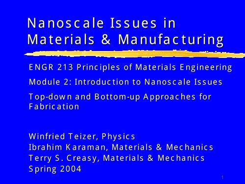
<strong>Nanoscale</strong> Issues in<br />
Materials & Manufacturing<br />
ENGR 213 Principles of Materials Engineering<br />
Module 2: Introduction <strong>to</strong> <strong>Nanoscale</strong> Issues<br />
<strong>Top</strong>-<strong>down</strong> <strong>and</strong> <strong>Bot<strong>to</strong>m</strong>-<strong>up</strong> <strong>Approaches</strong> for<br />
<strong>Fabrication</strong><br />
Winfried Teizer, Physics<br />
Ibrahim Karaman, Materials & Mechanics<br />
Terry S. Creasy, Materials & Mechanics<br />
Spring 2004<br />
1
Primer on manufacturing processes<br />
<strong>Bot<strong>to</strong>m</strong>-<strong>up</strong> self<br />
assembly (wet<br />
chemistry)<br />
biomimetic,<br />
controlled<br />
<strong>Top</strong>-<strong>down</strong> assembly<br />
(lithography <strong>and</strong><br />
derivatives)<br />
dip-pen pen lithography<br />
soft lithography <strong>and</strong><br />
nanoscale printing<br />
e-beam <strong>and</strong> deep<br />
UV lithography<br />
Other production<br />
processes<br />
vapor deposition<br />
evaporation<br />
combustion<br />
thermal plasma<br />
milling<br />
cavitation<br />
coating (spin or<br />
dip)<br />
thermal spray<br />
electrodeposition<br />
2-040503TSCD
Module 2: <strong>Nanoscale</strong> Issues<br />
<strong>Top</strong>-<strong>down</strong> <strong>Approaches</strong> <strong>to</strong><br />
<strong>Fabrication</strong><br />
<strong>Bot<strong>to</strong>m</strong>-<strong>up</strong> <strong>Approaches</strong> <strong>to</strong><br />
<strong>Fabrication</strong><br />
3-040503TSCD
Two principal approaches<br />
<strong>Top</strong>-Down<br />
Miniaturizing existing<br />
processes at the<br />
Macro/Microscale<br />
Traditional approach in<br />
industrial applications<br />
E.g. Lithography, backbone of<br />
computing systems<br />
<strong>Bot<strong>to</strong>m</strong>-Up<br />
Assembling structures from<br />
the a<strong>to</strong>mic/molecular level<br />
Novel approach, conceptually<br />
imitating nature<br />
E.g. chemical self-assembly<br />
4-040503TSCD
Two principal approaches<br />
<strong>Top</strong>-Down<br />
Miniaturizing existing<br />
processes at the<br />
Macro/Microscale<br />
Traditional approach in<br />
industrial applications<br />
E.g. Lithography, backbone of<br />
computing systems<br />
<strong>Bot<strong>to</strong>m</strong>-Up<br />
Assembling structures from<br />
the a<strong>to</strong>mic/molecular level<br />
Novel approach, conceptually<br />
imitating nature<br />
E.g. chemical self-assembly<br />
5-040503TSCD
<strong>Nanoscale</strong> Issues in Materials<br />
& Manufacturing<br />
<strong>Top</strong>-<strong>down</strong><br />
<strong>Approaches</strong> <strong>to</strong><br />
<strong>Fabrication</strong><br />
6
Lithography in the Arts<br />
• Invented by Alois Senefelder in 1798<br />
• Process has been used for book<br />
illustrations, artist's prints,<br />
packaging, posters etc.<br />
• In 1825, Goya produced a famous<br />
series of lithographs titled “The Bulls<br />
of Bordeaux”.<br />
• In the 20 th <strong>and</strong> 21 st century, becomes<br />
an important technique with unique<br />
expressive capabilities in the Art<br />
field.<br />
7-040503TSCD
How Lithography started<br />
Lithography (Greek for "s<strong>to</strong>ne<br />
drawing") relies on the fact that<br />
water <strong>and</strong> grease repel<br />
Draw a pattern on<strong>to</strong> a flat s<strong>to</strong>ne<br />
surface with a greasy substance<br />
Paint the printing ink on<strong>to</strong> the s<strong>to</strong>ne<br />
While the s<strong>to</strong>ne background<br />
absorbs water, the greasy<br />
substance retains wet ink on <strong>to</strong>p<br />
Press paper against the s<strong>to</strong>ne <strong>to</strong><br />
transfer the pattern<br />
Positive! Repeatable!<br />
8-040503TSCD
Lithography, <strong>to</strong> date<br />
Miniaturized computing circuits require mass<br />
manufacturing of small features ⇒ push<br />
lithographic approach <strong>to</strong> new limits<br />
Some lithography approaches for manufacturing<br />
Optical lithography (including ultraviolet)<br />
X-Ray lithography<br />
Electron Beam lithography<br />
Ion Beam lithography<br />
“Dip-Pen” lithography<br />
…<br />
9-040503TSCD
Optical/UV Lithography<br />
Workhorse of current chip manufacturing<br />
processes<br />
Limited by wave length of light employed<br />
Smaller features ⇒ reduce wave length ⇒ UV<br />
light<br />
Here is how it works<br />
10-040503TSCD<br />
040503TSCD
Optical Lithography<br />
Mask<br />
Pho<strong>to</strong>resist<br />
Si - Substrate<br />
11-040503TSCD
Optical Lithography<br />
12-040503TSCD
Optical Lithography<br />
13-040503TSCD
Optical Lithography<br />
14-040503TSCD
Example: Pentium III<br />
Low Magnification<br />
High Magnification<br />
15-040503TSCD
Lithography<br />
16-040503TSCD
Fundamental Limitations<br />
• Smallest Feature Size is limited by<br />
wave length of light used<br />
• Currently deep UV light is used <strong>to</strong> produce<br />
sub-µm line widths<br />
• Moving in<strong>to</strong> X-ray may allow further reduction<br />
• This has practical complications, e.g. lenses<br />
17-040503TSCD
X-Ray Lithography Example<br />
18-040503TSCD
E-Beam Lithography<br />
•Smallest Feature Size of<br />
optical lithography is limited<br />
by wave length of light<br />
• Use a smaller wave length!<br />
• Use electrons!<br />
• Quantum Mechanics ⇒ all<br />
particles have a wave length<br />
• Higher energy ⇒ lower<br />
wave length<br />
Example<br />
19-040503TSCD
Electron Beam Lithography<br />
20-040503TSCD<br />
040503TSCD
Electron Beam Lithography<br />
21-040503TSCD
Electron Beam Lithography<br />
22-040503TSCD
Electron Beam Lithography<br />
23-040503TSCD
Electron Beam Lithography<br />
24-040503TSCD
Electron Beam Lithography<br />
25-040503TSCD
Electron Beam Lithography<br />
26-040503TSCD
Current Capabilities<br />
• Use either dedicated e-beam writer or SEM (Vacuum<br />
environment)<br />
• 30nm line width is straightforward<br />
•
Ion Beam Lithography Example<br />
28-040503TSCD
Dip-Pen Lithography<br />
29-040503TSCD
dip-pen pen lithography<br />
30-040503TSCD<br />
040503TSCD
<strong>Nanoscale</strong> Issues in Materials<br />
& Manufacturing<br />
<strong>Bot<strong>to</strong>m</strong>-<strong>up</strong><br />
<strong>Approaches</strong> <strong>to</strong><br />
<strong>Fabrication</strong><br />
31
<strong>Bot<strong>to</strong>m</strong>-Up<br />
– Why?<br />
• <strong>Top</strong> <strong>down</strong> is reaching limits<br />
• Nature does not work <strong>to</strong>p-<strong>down</strong><br />
• Scientists like <strong>to</strong> imitate nature<br />
32-040503TSCD
<strong>Bot<strong>to</strong>m</strong>-Up<br />
– How?<br />
• Molecular Assembly<br />
•Self-Assembly<br />
• “Assisted” through external parameters<br />
(e.g. fields, catalysts, etc)<br />
• Biological Assembly<br />
33-040503TSCD
Self Assembly<br />
coordinated action of independent entities<br />
under distributed (i.e., non-central) control<br />
<strong>to</strong> produce a larger structure or <strong>to</strong> achieve a desired gro<strong>up</strong><br />
effect<br />
34-040503TSCD
Self Assembly<br />
Making What?<br />
35-040503TSCD
Self Assembly<br />
36-040503TSCD
37-040503TSCD
Self Assembly<br />
Other Self Assembly Areas<br />
Regular structured devices (optics)<br />
Nanocomposite fabrication<br />
Chemical sensors<br />
Wiring matrices (high density RAM)<br />
Chemical reac<strong>to</strong>rs<br />
Modular positioners<br />
Light-emitting diodes<br />
Optical s<strong>to</strong>rage materials<br />
Biosensors<br />
Drug-delivery materials<br />
38-040503TSCD
Ethical Consideration<br />
39-040503TSCD
Add Particles <strong>to</strong> Bulk<br />
Materials<br />
How do we keep<br />
‘nano’ character<br />
during processing?<br />
Consolidation of<br />
Metals<br />
Must stay below<br />
recrystallization<br />
temperatures.<br />
Mixing with Polymers<br />
Blend particles with<br />
resin or melted<br />
polymer.<br />
40-040503TSCD<br />
040503TSCD
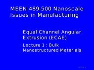
Equal Channel Angular<br />
Extrusion<br />
Solid state processing<br />
at low <strong>to</strong> room<br />
temperature.<br />
Intense plastic<br />
deformation in shear<br />
works the material.<br />
41-040503TSCD
Equal Channel Angular<br />
Extrusion<br />
42-040503TSCD
ECAE Effect<br />
Nanoparticles become<br />
bulk material with<br />
larger but nanoscale<br />
grain sizes.<br />
43-040503TSCD