Simulation of Lithography with SolidWorks - Foundation Coalition
Simulation of Lithography with SolidWorks - Foundation Coalition
Simulation of Lithography with SolidWorks - Foundation Coalition

Create successful ePaper yourself
Turn your PDF publications into a flip-book with our unique Google optimized e-Paper software.
SIMULATION OF LITHOGRAPHY/MEMS/NEMS BY SOLIDWORKSTerry S. Creasy, September 20, 2004INTRODUCTION.................................................................................................................................... 1PROCESS OVERVIEW ........................................................................................................................... 1PROCESSING STEPS.............................................................................................................................. 1Wafer ............................................................................................................................................. 2Color <strong>of</strong> Process Rule.................................................................................................................... 3Layer Addition Rule....................................................................................................................... 3Oxidation <strong>of</strong> Silicon (Oxide Mask) ................................................................................................ 3Photoresist ..................................................................................................................................... 4Expose/Develop ............................................................................................................................. 5MASK....................................................................................................................................................... 5Positive resist ............................................................................................................................................ 7Positive Mask....................................................................................................................................... 7Negative Mask ..................................................................................................................................... 8negative resist............................................................................................................................................ 9Negative Mask ..................................................................................................................................... 9Positive Mask..................................................................................................................................... 10Etch.............................................................................................................................................. 11Wet.......................................................................................................................................................... 11Isotropic ............................................................................................................................................. 11Orientation Dependent Etch (ODE) ................................................................................................... 11Boron Etch Stop (Mask) .................................................................................................................... 11Dry .......................................................................................................................................................... 11Argon Sputter Etch ............................................................................................................................ 11IntroductionThis is a work in progress. It defines steps for using solidworks s<strong>of</strong>tware forlithography process design and device modeling.Process Overview@Flow chart <strong>of</strong> process overview.Processing StepsEach step has a defined order <strong>of</strong> tasks and specific colors.040920TSCD_<strong>Simulation</strong>sSolidworksB.doc 1Last printed 3/13/2005 5:06 PM
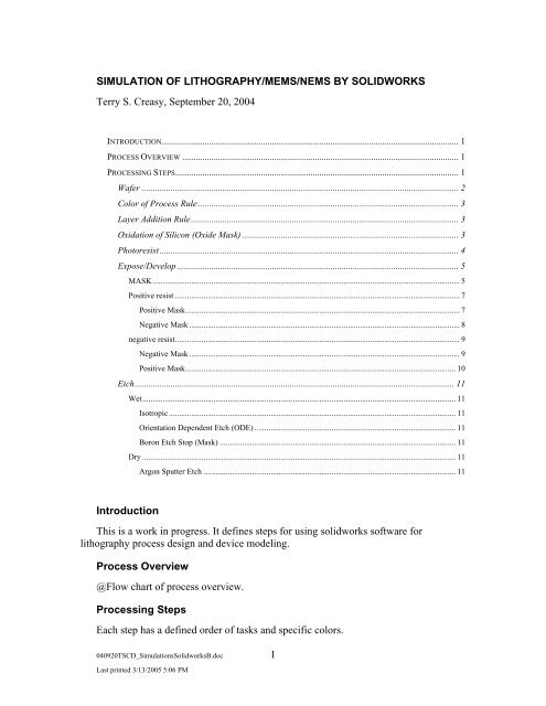
WaferThe color selections for wafers appear in Figure 1. Use a 25 mm square <strong>of</strong> Si wafer asyour design and build area. You may use a smaller area if this one is too big.Figure 1. Use the left color for n-type semiconductors and the right color for p-type.Name the wafer extrusion step and then set the color. @fig shows this.Figure 2. Left image: 25 mm square wafer. Right image: extrusion steprenamed.040920TSCD_<strong>Simulation</strong>sSolidworksB.doc 2Last printed 3/13/2005 5:06 PM
Figure 3. Set the color to the correct n or p type Si.Color <strong>of</strong> Process RuleWhen you add a layer, right click on that feature and set the Feature to the codedcolor <strong>of</strong> the material.When you cut through a layer set the color <strong>of</strong> that feature to the color <strong>of</strong> the layer!This will result in proper colors <strong>of</strong> the layer side walls.At your last step you need to select the final expose surfaces and color those the color<strong>of</strong> the material that is showing.Layer Addition RuleWhenever you add a layer, you must step in from the prior edge by 1 mm. Theseprovides you—and me—<strong>with</strong> a check <strong>of</strong> where your layers are.Oxidation <strong>of</strong> Silicon (Oxide Mask)Silicon oxidation consumes Si as Si0 2 forms. The thickness ratio <strong>of</strong> oxide to Si is1:0.44. We will use a ratio <strong>of</strong> 1:0.5 <strong>with</strong> an extrude method. Figure 4 shows red is thecolor <strong>of</strong> the oxide layer.040920TSCD_<strong>Simulation</strong>sSolidworksB.doc 3Last printed 3/13/2005 5:06 PM
Figure 4. Oxide layers must appear in red.Figure 5 shows the effect <strong>of</strong> midplane extrusion in the simulation. The wafer isthicker by only ½ <strong>of</strong> the oxide layer thickness.Figure 5. Midplane extrusion <strong>of</strong> an oxide layer. Left, 10µm layer is 5 µm abovethe original Si surface and 5 µm below the original surface—some Si is consumed.Right, the red oxide surface and the thickness <strong>of</strong> the wafer shown at scale. The SiO 2layer is named and there is a step <strong>of</strong> 1 mm from the outer edge.PhotoresistAdd a white layer for positive resist and add a black layer for a negative photoresist.Remember the layer addition rule. Use these thickness values:Spin RPM Photoresist Thickness (nm)1000 22003000 12506000 900A positive photoresist layer over SiO 2 appears in @fig.040920TSCD_<strong>Simulation</strong>sSolidworksB.doc 4Last printed 3/13/2005 5:06 PM
Figure 6. Positive photoresist over SiO 2 .Expose/DevelopPositive and negative resists must follow their own protocol.MASKDesign the mask in a separate solidworks file. Make your sketch on the Front plane.Figure 7 shows the location <strong>of</strong> the text icon in the Tools/Customize menu. For thisexample we will use a text mask.040920TSCD_<strong>Simulation</strong>sSolidworksB.doc 5Last printed 3/13/2005 5:06 PM
Figure 7. You might need to add the Text Icon to the Sketch bar.Figure 8. Left, this mask removes material between the letters and the outerboarder. Right, this make removes material <strong>with</strong>in the letters.040920TSCD_<strong>Simulation</strong>sSolidworksB.doc 6Last printed 3/13/2005 5:06 PM
POSITIVE RESISTPositive MaskFigure 9. Left, select the top <strong>of</strong> the oxide layer; right, paste the mask sketch.Figure 10. Left, align the mask sketch <strong>with</strong> the substrate; right, extrude/cut <strong>with</strong>the settings shown.040920TSCD_<strong>Simulation</strong>sSolidworksB.doc 7Last printed 3/13/2005 5:06 PM
Figure 11. The result <strong>of</strong> the process. Rename the extrude/cut as Expose/Developand use right click to change the color to the color <strong>of</strong> the cut surface—thisphotoresist is white. If you stop, color the final exposed surfaces in the materialcolor, which the right image shows.Negative MaskAny mask that has nested closed regions <strong>of</strong> more than two sets must be usedrepeatedly. In the first use the outer lines and first set <strong>of</strong> lines <strong>with</strong>in them are solid.Deeper nests <strong>of</strong> lines must be deleted or set as ‘construction’ lines. You paste in the maskas many times as needed to complete the exposure and development process.Figure 12. The inner portions <strong>of</strong> the negative mask must be set to constructionlines.040920TSCD_<strong>Simulation</strong>sSolidworksB.doc 8Last printed 3/13/2005 5:06 PM
Figure 13. This negative mask required two applications. Left, the result <strong>of</strong> thefirst extrude/cut; right, the result <strong>of</strong> the second extrude cut.Figure 14. Left, positive resist <strong>with</strong> positive mask; right, positive resist <strong>with</strong>negative mask.NEGATIVE RESISTTo get this to work you first select a negative or positive mask. Then use THEOTHER MASK!Negative Mask040920TSCD_<strong>Simulation</strong>sSolidworksB.doc 9Last printed 3/13/2005 5:06 PM
Figure 15. We want this mask. Light will not pass through the letters. Thatmeans the negative resist will set and remain after development. Therefore, use thepositive mask in solidworks.Figure 16. The ‘wrong’ mask generates the correct result for a negative resist.Positive MaskFigure 17. The ‘wrong’ mask generates the correct result for a negative resist<strong>with</strong> two Expose/Develop steps. The second step takes care <strong>of</strong> the As.040920TSCD_<strong>Simulation</strong>sSolidworksB.doc 10Last printed 3/13/2005 5:06 PM
EtchEtch chemical target specific materials.WETWet etches are aqueous solutions that chemically attack a surface.IsotropicThese etches attack a target material uniformly. Etch chemistry 1 :Solution Target Etch Rate (nm/min)HF 49% SiO2 2300Phosphosilicate Glass 3600Silicon etch Si 310Acetone Photoresist 4000You can use any material as a mask if the etchant does not attack that material. Insome processes Si, SiO2, photoresist, and SiN can act as a mask for some other material.The isotropic etch eats under the mask. We will simulate it as a straight etch.Simulate the isotropic etch by these steps:NOTE: Don’t etch the stepped edge <strong>of</strong> the wafer. Those layers are there for gradingand checks <strong>of</strong> your process. Only etch in the masked region.Apply the mask pattern to the layer that you wish to etch.Extrude cut Blind, into the layer for the layer depth.Orientation Dependent Etch (ODE)ODE attacks specific crystal planes. In Si the etch stops on the {111} planes andattacks the {100} planes 100 times faster. The draft angle is 54.7°.If you etch deep enough the Si cavity will converge at a point.Boron Etch Stop (Mask)DRYArgon Sputter Etch1 Kalpakjian040920TSCD_<strong>Simulation</strong>sSolidworksB.doc 11Last printed 3/13/2005 5:06 PM