Simulation of Lithography with SolidWorks - Foundation Coalition
Simulation of Lithography with SolidWorks - Foundation Coalition
Simulation of Lithography with SolidWorks - Foundation Coalition

Create successful ePaper yourself
Turn your PDF publications into a flip-book with our unique Google optimized e-Paper software.
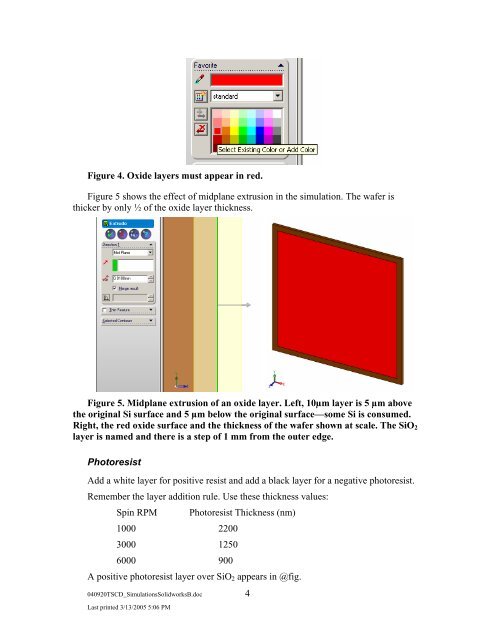
Figure 4. Oxide layers must appear in red.Figure 5 shows the effect <strong>of</strong> midplane extrusion in the simulation. The wafer isthicker by only ½ <strong>of</strong> the oxide layer thickness.Figure 5. Midplane extrusion <strong>of</strong> an oxide layer. Left, 10µm layer is 5 µm abovethe original Si surface and 5 µm below the original surface—some Si is consumed.Right, the red oxide surface and the thickness <strong>of</strong> the wafer shown at scale. The SiO 2layer is named and there is a step <strong>of</strong> 1 mm from the outer edge.PhotoresistAdd a white layer for positive resist and add a black layer for a negative photoresist.Remember the layer addition rule. Use these thickness values:Spin RPM Photoresist Thickness (nm)1000 22003000 12506000 900A positive photoresist layer over SiO 2 appears in @fig.040920TSCD_<strong>Simulation</strong>sSolidworksB.doc 4Last printed 3/13/2005 5:06 PM