Design Tip - IEEE EMC Society
Design Tip - IEEE EMC Society
Design Tip - IEEE EMC Society

Create successful ePaper yourself
Turn your PDF publications into a flip-book with our unique Google optimized e-Paper software.
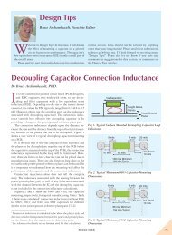
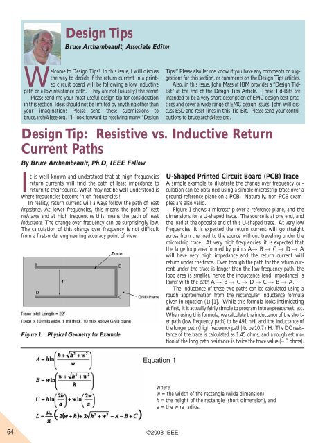
<strong>Design</strong> <strong>Tip</strong>s<br />
Bruce Archambeault, Associate Editor<br />
Welcome to <strong>Design</strong> <strong>Tip</strong>s! In this issue, I will discuss<br />
the way to decide if the return current in a printed<br />
circuit board will be following a low inductive<br />
path or a low resistance path. They are not (usually) the same!<br />
Please send me your most useful design tip for consideration<br />
in this section. Ideas should not be limited by anything other than<br />
your imagination! Please send these submissions to<br />
bruce.arch@ieee.org. I’ll look forward to receiving many “<strong>Design</strong><br />
<strong>Design</strong> <strong>Tip</strong>: Resistive vs. Inductive Return<br />
Current Paths<br />
By Bruce Archambeault, Ph.D, <strong>IEEE</strong> Fellow<br />
<strong>Tip</strong>s!” Please also let me know if you have any comments or suggestions<br />
for this section, or comments on the <strong>Design</strong> <strong>Tip</strong>s articles.<br />
Also, in this issue, John Maas of IBM provides a “<strong>Design</strong> Tid-<br />
Bit” at the end of the <strong>Design</strong> <strong>Tip</strong>s Article. These Tid-Bits are<br />
intended to be a very short description of <strong>EMC</strong> design best practices<br />
and cover a wide range of <strong>EMC</strong> design issues. John will discuss<br />
ESD and reset lines in this Tid-Bit. Please send your contributions<br />
to bruce.arch@ieee.org.<br />
It is well known and understood that at high frequencies<br />
return currents will find the path of least impedance to<br />
return to their source. What may not be well understood is<br />
where frequencies become ‘high frequencies’!<br />
In reality, return current will always follow the path of least<br />
impedance. At lower frequencies, this means the path of least<br />
resistance and at high frequencies this means the path of least<br />
inductance. The change over frequency can be surprisingly low.<br />
The calculation of this change over frequency is not difficult<br />
from a first-order engineering accuracy point of view.<br />
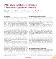
Figure 1. Physical Geometry for Example<br />
U-Shaped Printed Circuit Board (PCB) Trace<br />
A simple example to illustrate the change over frequency calculation<br />
can be obtained using a simple microstrip trace over a<br />
ground-reference plane on a PCB. Naturally, non-PCB examples<br />
are also valid.<br />
Figure 1 shows a microstrip over a reference plane, and the<br />
dimensions for a U-shaped trace. The source is at one end, and<br />
the load at the opposite end of this U-shaped trace. At very low<br />
frequencies, it is expected the return current will go straight<br />
across from the load to the source without traveling under the<br />
microstrip trace. At very high frequencies, it is expected that<br />
the large loop area formed by points A→ B → C → D → A<br />
will have very high impedance and the return current will<br />
return under the trace. Even though the path for the return current<br />
under the trace is longer than the low frequency path, the<br />
loop area is smaller, hence the inductance (and impedance) is<br />
lower with the path A → B → C → D → C → B → A.<br />
The inductance of these two paths can be calculated using a<br />
rough approximation from the rectangular inductance formula<br />
given in equation (1) [1]. While this formula looks intimidating<br />
at first, it is actually fairly simple to program into a spreadsheet, etc.<br />
When using this formula, we calculate the inductance of the shorter<br />
path (low frequency path) to be 491 nH, and the inductance of<br />
the longer path (high frequency path) to be 10.7 nH. The DC resistance<br />
of the trace is calculated as 1.45 ohms, and a rough estimation<br />
of the long path resistance is twice the trace value (~ 3 ohms).<br />
Equation 1<br />
where<br />
w = the width of the rectangle (wide dimension)<br />
h = the height of the rectangle (short dimension), and<br />
a = the wire radius.<br />
64<br />
©2008 <strong>IEEE</strong>
Figure 2 shows a calculation of the magnitude of the<br />
impedance for the inductances as well as the combined<br />
impedance for the resistance and inductance. Since the<br />
return current will always follow the path of least<br />
impedance, the cross over frequency is 800 KHz in this<br />
example. Below 800 KHz, the return current will take<br />
the shortest path, since it has the least resistance.<br />
Above 800 KHz, the majority of the return current will<br />
follow the longer path because it has less inductance.<br />
Summary<br />
The return current path will always find the path of least<br />
impedance. This impedance can be calculated to a first<br />
order approximation with a simple rectangular loop formula<br />
and the cross over frequency found quickly. <strong>EMC</strong><br />
[1] F.W. Gover, Inductance Calculations, Dover Publications,<br />
NY, 1946<br />
<strong>Design</strong> Tid-Bit<br />
ESD and Reset Lines<br />
Figure 2. Impedance of Return Current Paths for Long and Short<br />
Current Paths<br />
Keeping reset lines (for example, power on reset or processor reset) from reacting to ESD transients can be an interesting<br />
challenge. Proper system operation requires that these lines do not react to false triggers, but do respond to intended commands<br />
whose short duration can be similar to that of an ESD transient. In some cases, a simple pull up/down resistor paralleled<br />
with a small capacitor is sufficient to filter unwanted transients. The proper functioning on some circuits, however, will<br />
be impaired with the addition of even small values of capacitance. If any on-chip deglitching circuitry is not sufficient in these<br />
cases, firmware modifications to ignore the unwanted transients are often the only circuit-level solution.<br />
John Maas, IBM<br />
EMI/RFI Shielding Solutions<br />
Large inventory for immediate delivery<br />
Finest catalog in the industry: print and web<br />
Exceptional FREE sample program<br />
Work directly with the manufacturer<br />
Product specialists for application assistance<br />
Computerized quoting for instant pricing<br />
Highly skilled customer service<br />
Industry leader of innovative designs<br />
Customization of standard products<br />
Better than 99% quality rating<br />
ISO 9001:2000 Registered<br />
Visit our web site for<br />
a FREE SAMPLE!<br />
www.tech-etch.com/shield<br />
Tech-Etch, Inc.,<br />
©2008 <strong>IEEE</strong><br />
65