Decoupling Capacitor Connection Inductance - IEEE EMC Society
Decoupling Capacitor Connection Inductance - IEEE EMC Society
Decoupling Capacitor Connection Inductance - IEEE EMC Society

You also want an ePaper? Increase the reach of your titles
YUMPU automatically turns print PDFs into web optimized ePapers that Google loves.
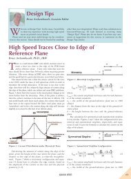
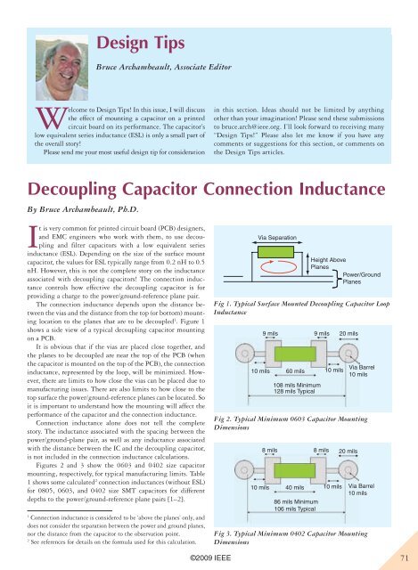
Design TipsBruce Archambeault, Associate EditorWelcome to Design Tips! In this issue, I will dis cussthe effect of mounting a capacitor on a printedcircuit board on its performance. The capacitor’slow equivalent series inductance (ESL) is only a small part ofthe overall story!Please send me your most useful design tip for considerationin this section. Ideas should not be limited by anythingother than your imagination! Please send these submissionsto bruce.arch@ieee.org. I’ll look forward to receiving many“Design Tips!” Please also let me know if you have anycomments or suggestions for this section, or comments onthe Design Tips articles.<strong>Decoupling</strong> <strong>Capacitor</strong> <strong>Connection</strong> <strong>Inductance</strong>By Bruce Archambeault, Ph.D.It is very common for printed circuit board (PCB) designers,and <strong>EMC</strong> engineers who work with them, to use decouplingand filter capacitors with a low equivalent seriesinductance (ESL). Depending on the size of the surface mountcapacitor, the values for ESL typically range from 0.2 nH to 0.5nH. However, this is not the complete story on the inductanceassociated with decoupling capacitors! The connection inductancecontrols how effective the decoupling capacitor is forproviding a charge to the power/ground-reference plane pair.The connection inductance depends upon the distance betweenthe vias and the distance from the top (or bottom) mountinglocation to the planes that are to be decoupled 1 . Figure 1shows a side view of a typical decoupling capacitor mountingon a PCB.It is obvious that if the vias are placed close together, andthe planes to be decoupled are near the top of the PCB (whenthe capacitor is mounted on the top of the PCB), the connectioninductance, represented by the loop, will be minimized. However,there are limits to how close the vias can be placed due tomanufacturing issues. There are also limits to how close to thetop surface the power/ground-reference planes can be located. Soit is important to understand how the mounting will affect theperformance of the capacitor and the connection inductance.<strong>Connection</strong> inductance alone does not tell the completestory. The inductance associated with the spacing between thepower/ground-plane pair, as well as any inductance associatedwith the distance between the IC and the decoupling capacitor,is not included in the connection inductance calculations.Figures 2 and 3 show the 0603 and 0402 size capacitormounting, respectively, for typical manufacturing limits. Table1 shows some calculated 2 connection inductances (without ESL)for 0805, 0603, and 0402 size SMT capacitors for differentdepths to the power/ground-reference plane pairs [1–2].1<strong>Connection</strong> inductance is considered to be ‘above the planes’ only, anddoes not consider the separation between the power and ground planes,nor the distance from the capacitor to the observation point.2See references for details on the formula used for this calculation.Via SeparationHeight AbovePlanesPower/GroundPlanesFig 1. Typical Surface Mounted <strong>Decoupling</strong> <strong>Capacitor</strong> Loop<strong>Inductance</strong>9 mils 9 mils 20 mils10 mils 10 mils60 mils108 mils Minimum128 mils TypicalVia Barrel10 milsFig 2. Typical Minimum 0603 <strong>Capacitor</strong> MountingDimensions8 mils 8 mils 20 mils10 mils 40 mils 10 mils Via Barrel10 mils86 mils Minimum106 mils TypicalFig 3. Typical Minimum 0402 <strong>Capacitor</strong> MountingDimensions©2009 <strong>IEEE</strong>71
Table 1. <strong>Connection</strong> <strong>Inductance</strong> for Typical <strong>Capacitor</strong> Configurations.Distance into boardto planes (mils)0805 typical/minimum(148 mils between via barrels)0603 typical/minimum(128 mils between via barrels)0402 typical/minimum(106 mils between via barrels)10 1.2 nH 1.1 nH 0.9 nH20 1.8 nH 1.6 nH 1.3 nH30 2.2 nH 1.9 nH 1.6 nH40 2.5 nH 2.2 nH 1.9 nH50 2.8 nH 2.5 nH 2.1 nH60 3.1 nH 2.7 nH 2.3 nH70 3.4 nH 3.0 nH 2.6 nH80 3.6 nH 3.2 nH 2.8 nH90 3.9 nH 3.5 nH 3.0 nH100 4.2 nH 3.7 nH 3.2 nHTable 2. <strong>Connection</strong> <strong>Inductance</strong> for Typical <strong>Capacitor</strong> Configurations with 50 mils from<strong>Capacitor</strong> Pad to Via Pad.Distance into boardto planes (mils)0805(208 mils between via barrels)0603(188 mils between via barrels)10 1.7 nH 1.6 nH 1.4 nH20 2.5 nH 2.3 nH 2.0 nH30 3.0 nH 2.8 nH 2.5 nH40 3.5 nH 3.2 nH 2.8 nH50 3.9 nH 3.5 nH 3.1 nH60 4.2 nH 3.9 nH 3.5 nH70 4.5 nH 4.2 nH 3.7 nH80 4.9 nH 4.5 nH 4.0 nH90 5.2 nH 4.7 nH 4.3 nH100 5.5 nH 5.0 nH 4.6 nH0402(166 mils between via barrels)These values are calculated with the example of 7–8 milsfrom capacitor-to-mounting-pad-edge, 20 mils from capacitormounting-pad-edge-to-via-pad,via pad diameter of 20 mils,via barrel size of 10 mils, and trace width equal to 20 mils.The absolute minimum distance from the via pad to capacitormounting pad edge is reported to be 10 mils, but typically 20mils is used to be ‘safe’.The distance between the via pad and the capacitor mountingpad was kept to a small value in the above calculations. Ifthis distance is increased slightly to 50 mils, the connectioninductance increases to the values shown in Table 2.SummaryThe connection inductance plays a much greater role in theperformance of decoupling capacitors than the typical ESL ofthese components. Typical connection inductance values ofone to three nanoHenries are typical with common surfacemount capacitor sizes and typical manufacturing technologies.Using the tables, engineers can decide if a decouplingcapacitor is better placed on the top or bottom surface of thePCB in order to best provide charge to the power/groundreferenceplane pairs.References[1] J. L. Knighten, B. Archambeault, J. Fan, S. Connor, and J. L. Drewniak.PDN design strategies: II. Ceramic SMT decoupling capacitors – Doeslocation matter?, <strong>IEEE</strong> <strong>EMC</strong> Soc. Newslett. (Winter 2006). Issue 208,pp. 56–67. Available: www.emcs.org[2] J. Fan, C. Wei, J. L. Drewniak, T. Van Doren, and J. L. Knighten,“Estimating the noise mitigating effect of local decoupling in printedcircuit boards,” <strong>IEEE</strong> Trans. Adv. Packag., vol. 25, no. 2, pp. 154–165,May 2002.<strong>EMC</strong>72 ©2009 <strong>IEEE</strong>