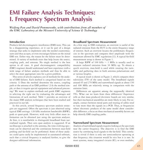
EMI Failure Analysis Techniques - IEEE EMC Society
EMI Failure Analysis Techniques - IEEE EMC Society
EMI Failure Analysis Techniques - IEEE EMC Society

You also want an ePaper? Increase the reach of your titles
YUMPU automatically turns print PDFs into web optimized ePapers that Google loves.
TABLE 1. OVERVIEW OF THE <strong>EMI</strong> ANALYSIS TECHNIQUES.Frequencyspectrumanalysis[2][3]Method Application For identifying ComplexityBroadbandmeasurementNarrowbandmeasurementZero spanmeasurementShort term FFT analysis [4]Correlation analysis [5][6]Resonanceanalysis [7]SweptfrequencymeasurementResonanceidentificationResonancescanningPort voltage and portimpedance measurementTransfer impedancemeasurementNear-field scanning [8][9][10]Current clamp and E/Hfield probe measurementTEM cell measurement[11] [12]SmalltechniquesObtainradiationpattern usingspectrumanalyzerUse strongmagnet toremove effectof a ferritePress and ob -serve amplitudechangeto distinguishcontact andproximity effectObtain an overview of the radiated emission.Distinguish between narrowband andbroadband signals.Analyze at very narrow span to identify finespectra details, e.g., sidebands, fordistinguishing between possible sources.For narrowband signal: differentiate AM orFM modulation. For broadband signal:determine switching frequencies.Reveal how a signal spectrum evolves withtime. Identify <strong>EMI</strong> sources from multiplebroadband sources in a complex system.Analyze mathematical correlation betweennear-field sources and far-field, or amongmultiple near-field observations.Investigate the resonance behavior bysubstituting a swept frequency clock for thesource.Use manual probing or near-field scanningto locate the resonance on a printed circuitboard (PCB) or metal structure.S21 scanning for each point on a PCB usinga cross probe to find local resonance andcoupling path.Measure between two metal parts on a PCBor enclosure to find suspected antennastructure and noise voltage.Quantify coupling path (coupling strengthfrom the source to other structures). Substitutean external signal for a possible <strong>EMI</strong> source.Use scanning system to obtain the E or H fielddistribution across the user-defined area onthe equipment under test (EUT).Measure common mode current on cables,then estimate far-field. Measure or injectE/H field on EUT.Determine the main <strong>EMI</strong> excitationmechanism: E or H field coupling. The boardhas 10 cm × 10 cm standard size.A quick view of the radiation pattern ofthe EUT.A fast method to remove the effect offerrite without physically changing thecircuit/board structure.Loose contact of metal connectors orproximity of noisy cables to metals maycause bad repeatability of <strong>EMI</strong> tests. Byobserving the magnitude in zero spanmeasurement, abrupt changes indicatecontact effect, while smooth changesindicate proximity effect.GeneralSourceSourceSourceSourceCouplingpath/antennaCouplingpath/antennaCoupling pathSource/coupling pathSource/coupling pathCoupling pathAntennaCoupling pathCoupling pathEasyEasyEasyComplexComplexModerateModerateComplexEasyComplexComplexModerateComplexEasyEasyEasy66 ©2009 <strong>IEEE</strong>
operate at the same frequency or with the same harmonics. Theunderlying idea is to identify subtle differences in the nearspectrum among signals having the same frequency and thencorrelate those differences to the far-field spectral signature.For example, in a phase locked loop (PLL), the reference signalfrom a crystal oscillator has very low phase noise and no sidebands.But the PLL might add phase noise and side bands. It issometimes possible to add a signal of e.g., 100 kHz to a clockto cause some phase modulation (i.e., periodic jitter, sidebands)in certain branches of a clock tree. If the 100 kHz sidebandsshow up in the radiated emissions, it can be concluded that theemissions are caused by the clock tree branches that containthe intended phase modulation, which is easy to detect, and inmany cases will not affect the functionality of the system.Figure 3 shows a narrowband measurement (100 Hz RBWand 6 kHz span) of the far-field radiation at 125 MHz from amother board. There are two signals very close in frequency:one is from the on-board clock, the other is PLL recovered fromLAN signal. In a broadband measurement, the two signals willshow up as one. To identify the signals, one method is to heatup the crystal oscillator in the LAN switch that provides theLAN signal to the PLL. The clock recovered from the incomingLAN will follow the drift of the crystal oscillator frequency.A data signal and clock signal provide another example.Data signal is more likely to be amplitude modulated whereasclocks are often phase modulated. Power supply variations maymodulate the PLL phase at the data frequency, thus data andclock have similar sideband structures, but one is phase modulatedand the other is amplitude modulated. Zero-span analysisor I/Q demodulation can differentiate between amplitude andphase modulation, even if the sideband magnitude is the same.Figure 4 shows the far-field signal from an EUT. The EUThas many clocks, but they are all phase locked to an 18 MHzreference. The insert in Figure 4 shows the near spectrum andsidebands of the harmonic centered at 144 MHz. Those sidebandsare usually visible at kHz or lower span setting. For eachharmonic, the measurement software captures not only its amplitudein 120 kHz RBW, but also its sidebands in a span setby the user, providing data for correlation between near-fieldand far-field.If it is not clear which IC is contributingto the far-field emission,Amplitude (dBm)–70–75–80–85–90–95the source can sometimes be identifiedby correlating the sidebandstructure of the far-field to the differentpossible ICs (more advancedcorrelation techniques for broadbandsignals will be addressed in alater article). Instead of the far-field,a current clamp is often used to measurecable current that determinesthe far-field; another option is thevoltage across a slot, if this slot isthe radiating antenna. The reasonfor substituting the far-field by arelevant near-field measurement isto avoid field changes caused by personstanding around the EUT whileprobing to find the best correlation.A really difficult <strong>EMI</strong> debuggingsituation occurs when a problematicradiation is caused by more than one antenna and couplingpath. In such situations counter-intuitive phenomena can beconfusing. For example, shielding a product may create strongerSemianechoic ChamberLog Periodic AntennaAmplifierSpectrumAnalyzerTurn TableDigital PhosphorOscilloscopeDUTPowerCordFig. 1. Typical far-field broadband measurement setup.E-Field (dBuV/m)555045403530FCC Radiated EmissionLimits for Class B Digital Devices25TV01TV02TV03200 200 400 600 800 1,000Frequency (MHz)Fig. 2. Far-field radiation measurement on three TVs.125 MHz Comparison Far Field125 MHz Main Clock125 MHz PLL Output125 MHZ Comparison Far Field–100125.002 125.003 125.004 125.005 125.006 125.007 125.008 125.009 125.01Frequency (MHz)Fig. 3. Narrowband measurement of the far-field radiation at 125 MHz from amother board.©2009 <strong>IEEE</strong>67
Amplitude (dBm)0–20–40–60–80Broadband Spectrum of a Clock SignalAmplitude (dBm)–40–45–50–55–60–65–70–75–80–85Narrowband Spectrum–90143.975 143.98143. 98514 3.99143.9 95 144 144.005 144.01 144.015 144.02 144.025Frequency (MHz)sidebands. We will observe the spectrumshown in Figure 6.If these two signals radiate fromdifferent antennas, the two antennaslikely have different radiationpatterns (Figure 7). In such a case,the sideband-to-carrier ratio will bea function of the antenna rotation.In Figure 8, the carrier signal is reducedby about 5 dB if the turntableis rotated from 86° to 191° but thesidebands remain at about -70 dB.Two sources, one with sidebands andone without, are emitted from differentantenna structures.–100–1200 100 200 300 400 500 600 700 800 900 1,000Frequency (MHz)Fig. 4. Super narrowband scan of the far-field signal from an EUT.Zero Span MeasurementTwo signals may have similar sidebandmagnitudes, but differentmodulations. Amplitude modulat ion(AM) cannot be distinguisheddirectly from small-angle frequencyemission! As an example, the <strong>EMI</strong> antenna receives the vectorsum of the signals. If two sources of similar magnitude reachthe antenna, they can constructively or destructively interfere.If they interfere destructively and one signal is shielded, thetotal signal will increase.When multiple sources transmit at the same frequency butdiffer in spectral details, the source can still be identified by carefullyanalyzing the narrowband spectrum of the far-field andcomparing it with that of locally measured signals. The case illustratedin Figure 4 shows how two potential <strong>EMI</strong> sources can bedifferentiated from sideband spectra. If the far-field is dominatedby a signal with sidebands, a modification will change both thecarrier and the sidebands. This is the case at 72 MHz (Figure 5).But at 252 MHz the situation is quite different. The signalreceived by the log-periodic antenna is a superposition of bothsources, and the modification affects only the signal withoutMagnitude (dBm)–55–60–65–70–75–80–85Example of Two Kinds of EmissionSource Show Constructive Combination EffectBefore ModificationAfter Modification–90251.97 251.98 251.99 252 252.01 252.02Frequency (MHz)–40BeforeAfter ModificationFig. 6. Far-field before and after a modification at 252MHz. Only the signal having no sidebands is reduced by themodification.Magnitude (dBm)–50–60–70–80Radiation Pattern ofSignal ATableRadiation Pattern ofSignal BInterfrenceRegion–9071.98 71.99 72 72.01 72.02Frequency (MHz)Fig. 5. Far-field before and after modification at 72 MHz.Main signal and sidebands change by the same amount.The far-field is dominated by the signal with sidebands.Fig. 7. Two sources distinguished by the sidebands patternhave different antenna structures, thus different radiationpatterns.68 ©2009 <strong>IEEE</strong>
(dB)–60–65–70–75–80–85–9586°191°287.99 288 288.01Frequency (MHz)Fig. 8. Far-field spectrum around 288 MHz for twoturn-table positions.Amplitude (dBm)Amplitude (dBm)–55RBW: 5 MHz; VBW: 5 MHz,Center:667.6 MHz, SPAN: 0 Hz–57.5–60–62.5–650 5 10 15 20 25 30 35 40 45 50Time (ms)–50–60–70–80–900 10 20 30 40 50 60 70 80 90 100Time (µs)Fig. 10. Zero span measurement data at 667.6 MHz with50 ms and 100 µs sweep time.E-Field (dBµV/m)2520151050–5RBW: 2 KHz; VBW: 2 KHz,Center: 667.6 MHz, SPAN: 10 MHz663 664 665 666 667 668 669 670 671 672modulation (FM). IQ demodulation or a time domain viewhelps. IQ demodulation is not implemented in many spectrumanalyzers, but zero span can reveal the amplitude demodulatedsignal, provided that the modulation frequency is less than halfof the largest RBW of the spectrum analyzer.The center frequency of the spectrum analyzer is set to thefrequency of interest using 0 Hz span, so that the horizontalaxis shows time instead of frequency. The RBW must be largerthan the spectrum occupied by the modulation, and the sweeptime needs to be adjusted to see the AM modulation.Typically, switched power supplies have switching frequenciesbetween 30 kHz and 3 MHz. Data stream AM modulationcan have a much broader range, whereas periodic jitter of PLLshas no amplitude modulation.Zero span measurement reveals how the amplitude changeswith time for any modulated RF signal within a specified bandwidth.Zero span measurement is quite useful to understandwhich switched power supply is causing a broadband noise. Inthe following case, an electronic device has a narrowband radiatedsignal centered at 667.6 MHz (Figure 9). The sidebandsof the signal are complex and unsymmetrical due to multiplesources and modulations. An ordinary spectrum measurementor time domain measurement cannot unravel the mixed signals.But zero span measurement reveals several switching activitiesof the complex signal under different sweep time settings. Figure10 shows two amplitude modulation signals: one with aperiodicity of 16.7 ms (from 60 Hz AC power supply) withdown-going pulses, the other with a periodicity of about 15 µs(from the 66.7 kHz switching frequency of one synchronousbuck converter). The next step would be using near field probingto locate the buck converter that switches at 66.7 kHz, andcompare or correlate the near field signal to the far field fordetermining the <strong>EMI</strong> source signal.Fig. 9. Spectrum of the 667.6 MHz radiated signal has verycomplex sidebands, together with some clock signals.ConclusionThis is the first article of a series covering different techniquesfor <strong>EMI</strong> failure analysis. It presented an overview of the <strong>EMI</strong>analysis techniques, and started with the basic measurementsthat can be done with a spectrum analyzer to obtain more informationrelative to the standard settings. The next article willcover time domain methods and the time varying spectral contentof signals.References[1] http://www.fcc.gov/oet/info/rules, FCC Rules & Regulations, May. 2009.[2] Application Notes, “Spectrum <strong>Analysis</strong> Basics: From 1997 Back to BasicsSeminar,” Agilent Technologies, 1997.[3] Werner Schaefer, “<strong>EMC</strong> Narrowband and Broadband Discrimination witha Spectrum Analyzer or <strong>EMI</strong> Receiver,” Conformity, Dec. 2007.[4] Zhe Li and Pommerenke, D., “<strong>EMI</strong>-debugging of complex systems usingdifferent time, modulation, STFFT and frequency domain signal analysistechniques,” <strong>IEEE</strong> International Symposium on Electromagnetic Compatibility,2005. vol. 2.[5] Parhami, P., Marino, M., Watkins, S., Nakauchi, E., “Innovative pre-compliancetest methodology using ambient cancellation and coherence detectiontechniques,” <strong>IEEE</strong> International Symposium on ElectromagneticCompatibility, 1999, vol. 2.[6] Gang Feng, Wei Wu, Pommerenke, D., Jun Fan, Beetner, D.G., “Timesynchronized near-field and far-field for <strong>EMI</strong> source identification,”©2009 <strong>IEEE</strong>69
<strong>IEEE</strong> International Symposium on Electromagnetic Compatibility,2008.[7] Kelander, I., Uusimaki, M., Arslan, A.N., Nokia Corp., Helsinki, “<strong>EMC</strong>analysis on stacked packages,” 17th International Zurich Symposium onElectromagnetic Compatibility, 2006.[8] D Pommerenke, G Muchaidze, J Koo, Q Cai, “Application and limits of ICand PCB scanning methods for immunity analysis,” 18th InternationalZurich Symposium on Electromagnetic Compatibility, 2007.[9] Muchaidze, G., Huang Wei, Jin Min, Shao Peng, Drewniak, J., Pommerenke,D., “Automated near-field scanning to identify resonances,” <strong>IEEE</strong>International Symposium on Electromagnetic Compatibility, 2008.[10] Muchaidze, G., Jayong Koo, Qing Cai, Tun Li, Lijun Han, Martwick, A.,Kai Wang, Jin Min, Drewniak, J.L., Pommerenke, D., “SusceptibilityScanning as a <strong>Failure</strong> <strong>Analysis</strong> Tool for System-Level Electrostatic Discharge(ESD) Problems,” <strong>IEEE</strong> Transactions on Electromagnetic Compatibility,May 2008, Volume: 50, Issue: 2[11] Deng Shaowei, Hubing, T., Beetner, D.G., “Characterizing the ElectricField Coupling from IC Heatsink Structures to External Cables Using T<strong>EMC</strong>ell Measurements,” <strong>IEEE</strong> Transactions on Electromagnetic Compatibility,Nov. 2007, Volume: 49, Issue: 4[12] S Deng, D Pommerenke, T Hubing, J Drewniak, “Mode Suppressed T<strong>EMC</strong>ell Design for High Frequency IC Measurements,” <strong>IEEE</strong> InternationalSymposium on Electromagnetic Compatibility, 2007.BiographiesDr. David Pommerenke received the Ph.D. from the Technical UniversityBerlin, Germany in 1996. After working at Hewlett Packard for fiveyears, he joined the Electromagnetic CompatibilityLaboratory at the University of Missouri Rolla in2001 where he is currently a tenured professor. Hehas published more than 100 papers and is an inventoron nine patents. In addition to other professionalactivities, he is the US representative of the ESDstandard setting group within the IEC TC77b. Heis a past Distinguished Lecturer for the <strong>IEEE</strong> <strong>EMC</strong><strong>Society</strong> (2006–2007). His research interests include system level ESD,numerical simulations, <strong>EMC</strong> measurement methods, and instrumentations.Weifeng Pan is currently an <strong>EMC</strong> designengineer at Google Inc., in Mountain View,California. He received his Ph.D. in May 2009at the Electromagnetic Compatibility Laboratoryof the Missouri University of Science & Technology.He was an intern at IBM in ResearchTriangle Park, North Carolina, from May toNovember 2008. He worked as RF design engineerat UTStarcom (China) from 2002 to 2005. He received hisBSEE in 1999 and MSEE in 2002 from Tsinghua University, Beijing,China. His research interests include electromagnetics, <strong>EMC</strong>, andsignal integrity.<strong>EMC</strong>