Design Tips - IEEE EMC Society
Design Tips - IEEE EMC Society
Design Tips - IEEE EMC Society

Create successful ePaper yourself
Turn your PDF publications into a flip-book with our unique Google optimized e-Paper software.
<strong>Design</strong> <strong>Tips</strong><br />
Bruce Archambeault, Associate Editor<br />
Welcome to <strong>Design</strong> <strong>Tips</strong>! In this issue, I would like<br />
to share my experience with locating high speed<br />
traces on printed circuit boards.<br />
Please send me your most useful design tip for consideration<br />
in this section. Ideas should not be limited by anything<br />
other than your imagination! Please send these submissions to<br />
bruce.arch@ieee.org. I’ll look forward to receiving many<br />
“<strong>Design</strong> <strong>Tips</strong>!” Please also let me know if you have any comments<br />
or suggestions for this section, or comments on the<br />
<strong>Design</strong> <strong>Tips</strong> articles.<br />
High Speed Traces Close to Edge of<br />
Reference Plane<br />
Bruce Archambeault, Ph.D., IBM<br />
There is a well known <strong>EMC</strong> rule which cautions never to<br />
route a trace too close to the edge of the PCB board<br />
and/or reference plane. I have seen rules that state the<br />
trace should be no closer than 500 mils, others requiring greater<br />
distances. Like most things in <strong>EMC</strong> rules, there is a grey area,<br />
and the good/bad of a particular distance is not black and white.<br />
The reason for this rule is that the return current for the trace<br />
is not 100% under the trace; it will spread out a little in order to<br />
minimize the overall inductance. If the trace is too close to the<br />
edge, then there will be a relatively large amount of current along<br />
the edge of the plane, which can radiate and cause <strong>EMC</strong> problems.<br />
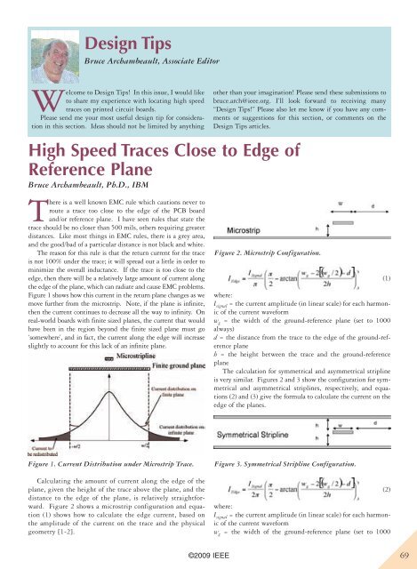
Figure 1 shows how this current in the return plane changes as we<br />
move further from the microstrip. Note, if the plane is infinite,<br />
then the current continues to decrease all the way to infinity. On<br />
real-world boards with finite sized planes, the current that would<br />
have been in the region beyond the finite sized plane must go<br />
‘somewhere’, and in fact, the current along the edge will increase<br />
slightly to account for this lack of an infinite plane.<br />
Figure 2. Microstrip Configuration.<br />
where:<br />
I signal = the current amplitude (in linear scale) for each harmonic<br />
of the current waveform<br />
w g = the width of the ground-reference plane (set to 1000<br />
always)<br />
d = the distance from the trace to the edge of the ground-reference<br />
plane<br />
h = the height between the trace and the ground-reference<br />
plane<br />
The calculation for symmetrical and asymmetrical stripline<br />
is very similar. Figures 2 and 3 show the configuration for symmetrical<br />
and asymmetrical striplines, respectively, and equations<br />
(2) and (3) give the formula to calculate the current on the<br />
edge of the planes.<br />
(1)<br />
Figure 1. Current Distribution under Microstrip Trace.<br />
Calculating the amount of current along the edge of the<br />
plane, given the height of the trace above the plane, and the<br />
distance to the edge of the plane, is relatively straightforward.<br />
Figure 2 shows a microstrip configuration and equation<br />
(1) shows how to calculate the edge current, based on<br />
the amplitude of the current on the trace and the physical<br />
geometry [1-2].<br />
Figure 3. Symmetrical Stripline Configuration.<br />
where:<br />
I signal = the current amplitude (in linear scale) for each harmonic<br />
of the current waveform<br />
w g = the width of the ground-reference plane (set to 1000<br />
(2)<br />
©2009 <strong>IEEE</strong><br />
69
always)<br />
d = the distance from the trace to the edge of the ground-reference<br />
plane<br />
h = the height between the trace and the ground-reference plane<br />
Figure 4. Asymmetrical Stripline Configuration.<br />
(3a)<br />
(3b)<br />
where:<br />
I signal = the current amplitude (in linear scale) for each harmonic<br />
of the current waveform<br />
w g = the width of the ground-reference plane (set to 1000<br />
always)<br />
d = the distance from the trace to the edge of the ground-reference<br />
plane<br />
h 1 and h 2 = the height between the trace and the ground-reference<br />
plane<br />
Figure 5 shows a plot of the current on the edge for the<br />
microstrip and symmetrical stripline normalized to the current<br />
on the trace.<br />
How Much is Too Much?<br />
This is a difficult question to answer without a lot of detailed<br />
analysis of the PCB configuration. However, we can get an<br />
order of magnitude using some simple analysis. If we consider<br />
the edge of the reference plane as a thin wire antenna when<br />
looking at the edge view (similar to a dipole antenna), and<br />
looking at the most efficient radiation model, we can use a halfwave<br />
dipole model. The far field for a half-wave dipole is given<br />
in equation (4).<br />
where:<br />
E φ = Electric Field (V/m)<br />
I = current amplitude (A)<br />
r = distance to observation point (meters)<br />
θ = angle from dipole to observation point<br />
Let’s take an example where the fundamental harmonic frequency<br />
has an amplitude of 10 ma and the microstrip trace is 10<br />
(4)<br />
Figure 5. Normalized Current on Edge of Reference Plane.<br />
mils above the plane, and 300 mils from the edge of the plane<br />
(distance/height = 30). From Figure 5 we see the normalized<br />
edge current will be 40 dB less than the trace current, giving us<br />
100 µa of current along the edge of the plane. Using this value<br />
of current, and maximizing the angle, we will have ~ 71.5<br />
dBµV/m at 10 meters from the edge of the plane. We can use<br />
this very approximate value to very roughly determine the<br />
amount of shielding that may be required to meet emissions<br />
standards. We can also see that if we are able to move the trace<br />
further from the edge to 3000 mils (ratio of 300), we can see<br />
that we will reduce the current along the edge (and the radiated<br />
emissions) by 20 dB for this potential issue.<br />
Summary<br />
This article shows how to do some rough calculations to determine<br />
the effect of a trace’s distance to the edge of the reference<br />
plane. The emissions calculation is very rough, and should<br />
only be used with extreme care. For example, if the length of<br />
the board is much smaller than a half-wave length, the dipole<br />
equation is not appropriate (but will provide a worst case<br />
result). The emissions will be directly proportional to the<br />
amplitude of the current along the edge of the plane, so reducing<br />
the current will have a corresponding reduction in the<br />
emissions for this potential issue.<br />
References:<br />
[1] M.Y. Koledintseva, J.L. Drewniak, T.P. Van Doren, D.J.<br />
Pommerenke, M. Cocchini, and D.M. Hockanson,<br />
“Method of edge currents for calculating mutual external<br />
inductance in a microstrip structure,” Progress in Electromagnetic<br />
Research (PIER), Vol. 80, Jan. 2008, pp. 197-<br />
224.<br />
[2] M.Y. Koledintseva, J.L. Drewniak, T.P. Van Doren, D.J.<br />
Pommerenke, M. Cocchini, and D.M. Hockanson, “Mutual<br />
external inductance in stripline structures,” Progress in<br />
Electromagnetic Research (PIER), Vol. 80, Jan. 2008, pp.<br />
349-368. <strong>EMC</strong><br />
70<br />
©2009 <strong>IEEE</strong>