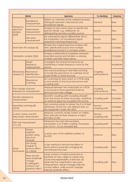
TABLE 1. OVERVIEW OF THE <strong>EMI</strong> ANALYSIS TECHNIQUES.Frequencyspectrumanalysis[2][3]Method Application For identifying ComplexityBroadbandmeasurementNarrowbandmeasurementZero spanmeasurementShort term FFT analysis [4]Correlation analysis [5][6]Resonanceanalysis [7]SweptfrequencymeasurementResonanceidentificationResonancescanningPort voltage and portimpedance measurementTransfer impedancemeasurementNear-field scanning [8][9][10]Current clamp and E/Hfield probe measurementTEM cell measurement[11] [12]SmalltechniquesObtainradiationpattern usingspectrumanalyzerUse strongmagnet toremove effectof a ferritePress and ob -serve amplitudechangeto distinguishcontact andproximity effectObtain an overview of the radiated emission.Distinguish between narrowband andbroadband signals.Analyze at very narrow span to identify finespectra details, e.g., sidebands, fordistinguishing between possible sources.For narrowband signal: differentiate AM orFM modulation. For broadband signal:determine switching frequencies.Reveal how a signal spectrum evolves withtime. Identify <strong>EMI</strong> sources from multiplebroadband sources in a complex system.Analyze mathematical correlation betweennear-field sources and far-field, or amongmultiple near-field observations.Investigate the resonance behavior bysubstituting a swept frequency clock for thesource.Use manual probing or near-field scanningto locate the resonance on a printed circuitboard (PCB) or metal structure.S21 scanning for each point on a PCB usinga cross probe to find local resonance andcoupling path.Measure between two metal parts on a PCBor enclosure to find suspected antennastructure and noise voltage.Quantify coupling path (coupling strengthfrom the source to other structures). Substitutean external signal for a possible <strong>EMI</strong> source.Use scanning system to obtain the E or H fielddistribution across the user-defined area onthe equipment under test (EUT).Measure common mode current on cables,then estimate far-field. Measure or injectE/H field on EUT.Determine the main <strong>EMI</strong> excitationmechanism: E or H field coupling. The boardhas 10 cm × 10 cm standard size.A quick view of the radiation pattern ofthe EUT.A fast method to remove the effect offerrite without physically changing thecircuit/board structure.Loose contact of metal connectors orproximity of noisy cables to metals maycause bad repeatability of <strong>EMI</strong> tests. Byobserving the magnitude in zero spanmeasurement, abrupt changes indicatecontact effect, while smooth changesindicate proximity effect.GeneralSourceSourceSourceSourceCouplingpath/antennaCouplingpath/antennaCoupling pathSource/coupling pathSource/coupling pathCoupling pathAntennaCoupling pathCoupling pathEasyEasyEasyComplexComplexModerateModerateComplexEasyComplexComplexModerateComplexEasyEasyEasy66 ©2009 <strong>IEEE</strong>
operate at the same frequency or with the same harmonics. Theunderlying idea is to identify subtle differences in the nearspectrum among signals having the same frequency and thencorrelate those differences to the far-field spectral signature.For example, in a phase locked loop (PLL), the reference signalfrom a crystal oscillator has very low phase noise and no sidebands.But the PLL might add phase noise and side bands. It issometimes possible to add a signal of e.g., 100 kHz to a clockto cause some phase modulation (i.e., periodic jitter, sidebands)in certain branches of a clock tree. If the 100 kHz sidebandsshow up in the radiated emissions, it can be concluded that theemissions are caused by the clock tree branches that containthe intended phase modulation, which is easy to detect, and inmany cases will not affect the functionality of the system.Figure 3 shows a narrowband measurement (100 Hz RBWand 6 kHz span) of the far-field radiation at 125 MHz from amother board. There are two signals very close in frequency:one is from the on-board clock, the other is PLL recovered fromLAN signal. In a broadband measurement, the two signals willshow up as one. To identify the signals, one method is to heatup the crystal oscillator in the LAN switch that provides theLAN signal to the PLL. The clock recovered from the incomingLAN will follow the drift of the crystal oscillator frequency.A data signal and clock signal provide another example.Data signal is more likely to be amplitude modulated whereasclocks are often phase modulated. Power supply variations maymodulate the PLL phase at the data frequency, thus data andclock have similar sideband structures, but one is phase modulatedand the other is amplitude modulated. Zero-span analysisor I/Q demodulation can differentiate between amplitude andphase modulation, even if the sideband magnitude is the same.Figure 4 shows the far-field signal from an EUT. The EUThas many clocks, but they are all phase locked to an 18 MHzreference. The insert in Figure 4 shows the near spectrum andsidebands of the harmonic centered at 144 MHz. Those sidebandsare usually visible at kHz or lower span setting. For eachharmonic, the measurement software captures not only its amplitudein 120 kHz RBW, but also its sidebands in a span setby the user, providing data for correlation between near-fieldand far-field.If it is not clear which IC is contributingto the far-field emission,Amplitude (dBm)–70–75–80–85–90–95the source can sometimes be identifiedby correlating the sidebandstructure of the far-field to the differentpossible ICs (more advancedcorrelation techniques for broadbandsignals will be addressed in alater article). Instead of the far-field,a current clamp is often used to measurecable current that determinesthe far-field; another option is thevoltage across a slot, if this slot isthe radiating antenna. The reasonfor substituting the far-field by arelevant near-field measurement isto avoid field changes caused by personstanding around the EUT whileprobing to find the best correlation.A really difficult <strong>EMI</strong> debuggingsituation occurs when a problematicradiation is caused by more than one antenna and couplingpath. In such situations counter-intuitive phenomena can beconfusing. For example, shielding a product may create strongerSemianechoic ChamberLog Periodic AntennaAmplifierSpectrumAnalyzerTurn TableDigital PhosphorOscilloscopeDUTPowerCordFig. 1. Typical far-field broadband measurement setup.E-Field (dBuV/m)555045403530FCC Radiated EmissionLimits for Class B Digital Devices25TV01TV02TV03200 200 400 600 800 1,000Frequency (MHz)Fig. 2. Far-field radiation measurement on three TVs.125 MHz Comparison Far Field125 MHz Main Clock125 MHz PLL Output125 MHZ Comparison Far Field–100125.002 125.003 125.004 125.005 125.006 125.007 125.008 125.009 125.01Frequency (MHz)Fig. 3. Narrowband measurement of the far-field radiation at 125 MHz from amother board.©2009 <strong>IEEE</strong>67