CMOS Technology MOSFETS: Gain & non-linearity ... - 6.004 - MIT
CMOS Technology MOSFETS: Gain & non-linearity ... - 6.004 - MIT
CMOS Technology MOSFETS: Gain & non-linearity ... - 6.004 - MIT

Create successful ePaper yourself
Turn your PDF publications into a flip-book with our unique Google optimized e-Paper software.
NEXT WEEK:<br />
• THU: Lab 1 due!<br />
• FRI: QUIZ 1!!!<br />
poly<br />
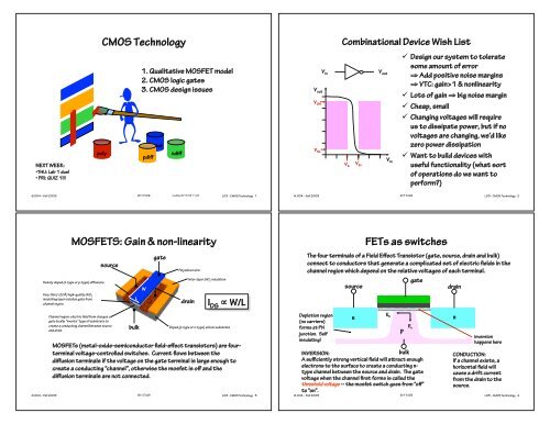
<strong>CMOS</strong> <strong>Technology</strong><br />
1. Qualitative MOSFET model<br />
2. <strong>CMOS</strong> logic gates<br />
3. <strong>CMOS</strong> design issues<br />
pdiff<br />
metal<br />
ndiff<br />
V out<br />
V OH<br />
V in<br />
V OL<br />
V IL<br />
V IH<br />
Combinational Device Wish List<br />
V out<br />
V in<br />
! Design our system to tolerate<br />
some amount of error<br />
! Add positive noise margins<br />
! VTC: gain>1 & <strong>non</strong><strong>linearity</strong><br />
! Lots of gain ! big noise margin<br />
! Cheap, small<br />
! Changing voltages will require<br />
us to dissipate power, but if no<br />
voltages are changing, we’d like<br />
zero power dissipation<br />
! Want to build devices with<br />
useful functionality (what sort<br />
of operations do we want to<br />
perform?)<br />
<strong>6.004</strong> – Fall 2009 9/17/09<br />
modified 9/17/09 11:20<br />
L03 - <strong>CMOS</strong> <strong>Technology</strong> 1<br />
<strong>6.004</strong> – Fall 2009 9/17/09<br />
L03 - <strong>CMOS</strong> <strong>Technology</strong> 2<br />
<strong>MOSFETS</strong>: <strong>Gain</strong> & <strong>non</strong>-<strong>linearity</strong><br />
Heavily doped (n-type or p-type) diffusions<br />
Very thin (
NFET: n-type source/drain<br />
diffusions in a p-type substrate.<br />
Positive threshold voltage;<br />
inversion forms n-type channel<br />
G<br />
B<br />
S<br />
n<br />
D<br />
S<br />
B<br />
G<br />
p<br />
FETs come in two flavors<br />
The use of both NFETs and PFETs – complimentary transistor types – is a key<br />
to <strong>CMOS</strong> (complementary MOS) logic families.<br />
<strong>6.004</strong> – Fall 2009 9/17/09<br />
D<br />
n<br />
Connect B to<br />
GND to keep PN<br />
reverse-biased<br />
(Vp < Vn); keeps<br />
D and S<br />
insulated from B<br />
PFET: p-type source/drain<br />
diffusions in a n-type substrate.<br />
Negative threshold voltage;<br />
inversion forms p-type channel.<br />
G<br />
B<br />
S<br />
p<br />
S<br />
B<br />
D<br />
G<br />
n<br />
D<br />
p<br />
Connect B to<br />
VDD to keep<br />
PN reversebiased<br />
L03 - <strong>CMOS</strong> <strong>Technology</strong> 5<br />
<strong>CMOS</strong> Recipe<br />
If we follow two rules when constructing <strong>CMOS</strong> circuits then we can model the<br />
behavior of the mosfets as simple switches:<br />
Rule #1: only use NFETs in pulldown circuits (paths from output node to GND)<br />
Rule #2: only use PFETs in pullup circuits (paths from output node to V DD )<br />
G<br />
S<br />
D<br />
S<br />
NFET Operating regions:<br />
“off”:<br />
V G < V TH,NFET<br />
“on”:<br />
V G > V TH,NFET<br />
S<br />
“ “<br />
<strong>6.004</strong> – Fall 2009 9/17/09<br />
D<br />
D<br />
G<br />
PFET Operating regions:<br />
“off”:<br />
V G > V DD + V TH,PFET<br />
“on”:<br />
V G < V DD + V TH,PFET<br />
~V DD /5 ~ -V TH,NFET<br />
S<br />
D<br />
S<br />
S<br />
“ “<br />
D<br />
D<br />
L03 - <strong>CMOS</strong> <strong>Technology</strong> 6<br />
When V IN is low, the<br />
nfet is off and the pfet<br />
is on, so current flows<br />
into the output node<br />
and V OUT eventually<br />
reaches V DD (= V OH ) at<br />
which point no more<br />
current will flow.<br />
pfet “on”<br />
nfet “off”<br />
<strong>CMOS</strong> Inverter VTC<br />
V out<br />
V OH<br />
V OL<br />
V IL<br />
V IH<br />
<strong>6.004</strong> – Fall 2009 9/17/09<br />
I pu<br />
I pd<br />
Steady state reached<br />
when V out reaches value<br />
where I pu = I pd .<br />
V in<br />
When V IN is high, the<br />
pfet is off and the nfet<br />
is on, so current flows<br />
out of the output node<br />
and V OUT eventually<br />
reaches GND (= V OL ) at<br />
which point no more<br />
current will flow.<br />
pfet “off”<br />
nfet “on”<br />
When VIN is in the middle, both the pfet and nfet are “on” and the shape of the VTC<br />
depends on the details of the devices’ characteristics. <strong>CMOS</strong> gates have very high gain<br />
in this region (small changes in V IN produce large changes in V OUT ) and the VTC is almost a<br />
step function.<br />
L03 - <strong>CMOS</strong> <strong>Technology</strong> 7<br />
Beyond Inverters:<br />
Complementary pullups and pulldowns<br />
<strong>6.004</strong> – Fall 2009 9/17/09<br />
Now you know what the “C”<br />
in <strong>CMOS</strong> stands for!<br />
We want complementary pullup and pulldown logic, i.e., the<br />
pulldown should be “on” when the pullup is “off” and vice<br />
versa.<br />
pullup pulldown F(A 1 ,…,An)<br />
on off driven “1”<br />
off on driven “0”<br />
on on driven “X”<br />
off off no connection<br />
Since there’s plenty of capacitance on the output node, when the output<br />
becomes disconnected it “remembers” its previous voltage -- at least<br />
for a while. The “memory” is the load capacitor’s charge. Leakage<br />
currents will cause eventual decay of the charge (that’s why DRAMs<br />
need to be refreshed!).<br />
L03 - <strong>CMOS</strong> <strong>Technology</strong> 8
What a nice<br />
V OH you have...<br />
<strong>CMOS</strong> complements<br />
A pop quiz!<br />
Thanks. It runs<br />
in the family...<br />
conducts when V GS is high<br />
A<br />
B<br />
conducts when A is high<br />
and B is high: A . B<br />
conducts when V GS is low<br />
A<br />
B<br />
conducts when A is low<br />
or B is low: A+B = A . B<br />
82#<br />
A<br />
B<br />
What function does<br />
this gate compute?<br />
A B<br />
0 0<br />
0 1<br />
1 0<br />
1 1<br />
C<br />
1<br />
1 NAND<br />
1<br />
0<br />
A<br />
B<br />
conducts when A is high<br />
or B is high: A+B<br />
A<br />
B<br />
conducts when A is low<br />
and B is low: A . B = A+B<br />
16#<br />
Current technology: # = 45nm<br />
COST:<br />
• $3500 per 300mm wafer<br />
• 300mm round wafer = $(150e -3 ) 2 = .07m 2<br />
• NAND gate = (82)(16)(45e -9 ) 2 =2.66e -12 m 2<br />
• 2.6e 10 NAND gates/wafer (= 100 billion FETS!)<br />
• marginal cost of NAND gate: 132n$<br />
<strong>6.004</strong> – Fall 2009 9/17/09<br />
L03 - <strong>CMOS</strong> <strong>Technology</strong> 9<br />
<strong>6.004</strong> – Fall 2009 9/17/09<br />
L03 - <strong>CMOS</strong> <strong>Technology</strong> 10<br />
Here’s another…<br />
General <strong>CMOS</strong> gate recipe<br />
B<br />
What function does<br />
this gate compute?<br />
Step 1. Figure out pulldown network that<br />
does what you want, e.g., F = A•(B +C)<br />
(What combination of inputs<br />
generates a low output)<br />
B<br />
A<br />
C<br />
A<br />
A B<br />
0 0<br />
0 1<br />
1 0<br />
1 1<br />
C<br />
1<br />
0 NOR<br />
0<br />
0<br />
Step 2. Walk the hierarchy ! replacing nfets<br />
with pfets, series subnets with parallel<br />
subnets, and parallel subnets with series<br />
subnets<br />
Step 3. Combine pfet pullup network<br />
from Step 2 with nfet pulldown<br />
network from Step 1 to form fullycomplementary<br />
<strong>CMOS</strong> gate.<br />
A<br />
A<br />
A<br />
B<br />
B<br />
C<br />
B<br />
C<br />
C<br />
So, whats the big<br />
deal?<br />
<strong>6.004</strong> – Fall 2009 9/17/09<br />
L03 - <strong>CMOS</strong> <strong>Technology</strong> 11<br />
<strong>6.004</strong> – Fall 2009 9/17/09<br />
L03 - <strong>CMOS</strong> <strong>Technology</strong> 12
A Quick Review<br />
Big Issue 1: Time<br />
Static<br />
discipline<br />
• A combinational device is a circuit element that has<br />
– one or more digital inputs<br />
– one or more digital outputs<br />
– a functional specification that details the value of each output for<br />
every possible combination of valid input values<br />
– a timing specification consisting (at minimum) of an upper bound<br />
t PD on the required time for the device to compute the specified<br />
output values from an arbitrary set of stable, valid input values<br />
V IN<br />
V out<br />
R<br />
C<br />
V IN<br />
input A<br />
input B<br />
input C<br />
If C is 1 then copy A to Y,<br />
otherwise copy B to Y<br />
I will generate a valid<br />
output in no more than<br />
2 weeks after<br />
seeing valid inputs<br />
output Y<br />
Wire delays:<br />
% RC ≈ 50ps/mm<br />
Implies > 1 ns to traverse a 20mm x 20mm chip<br />
This is a long time in a 2GHz processor<br />
<strong>6.004</strong> – Fall 2009 9/17/09<br />
L03 - <strong>CMOS</strong> <strong>Technology</strong> 13<br />
<strong>6.004</strong> – Fall 2009 9/17/09<br />
L03 - <strong>CMOS</strong> <strong>Technology</strong> 14<br />
Due to unavoidable delays…<br />
Propagation delay (t PD ):<br />
An UPPER BOUND on the delay from valid inputs<br />
to valid outputs.<br />
V IN<br />
V IH<br />
V IL<br />
V OUT<br />
V OH<br />
V OL<br />
< t PD<br />
<strong>6.004</strong> – Fall 2009 9/17/09<br />
< tPD<br />
GOAL:<br />
minimize<br />
propagation<br />
delay!<br />
ISSUE:<br />
keep<br />
Capacitances<br />
low and<br />
transistors<br />
fast<br />
time constant<br />
% = R PD •C L<br />
time constant&<br />
Contamination Delay<br />
an optional, additional timing spec<br />
INVALID inputs take time to propagate, too...<br />
V IN<br />
V IH Do we really need t CD ?<br />
V IL<br />
V OUT<br />
V OH<br />
V OL<br />
> t CD<br />
CONTAMINATION DELAY, t CD<br />
A LOWER BOUND on the delay from any invalid input to an invalid output<br />
% = R PU •C L<br />
L03 - <strong>CMOS</strong> <strong>Technology</strong> 15<br />
<strong>6.004</strong> – Fall 2009 9/17/09<br />
L03 - <strong>CMOS</strong> <strong>Technology</strong> 16<br />
> t CD<br />
Usually not… it’ll be<br />
important when we<br />
design circuits with<br />
registers (coming<br />
soon!)<br />
If t CD is not specified,<br />
safe to assume it’s 0.
The Combinational Contract<br />
Acyclic Combinational Circuits<br />
A<br />
B<br />
A<br />
B<br />
A B<br />
0 1<br />
1 0<br />
t PD propagation delay<br />
t CD contamination delay<br />
If NAND gates have a t PD = 4nS and t CD = 1nS<br />
t CD is the minimum cumulative<br />
contamination delay over all<br />
paths from inputs to outputs<br />
B<br />
t PD = _______ 12 nS<br />
t CD = _______ 2 nS<br />
Must be ___________<br />
C<br />
Y<br />
Note:<br />
1. No Promises during<br />
2. Default (conservative) spec: t CD = 0<br />
Must be ___________ < t PD<br />
> t CD L03 - <strong>CMOS</strong> <strong>Technology</strong> 18<br />
A<br />
t PD is the maximum cumulative<br />
propagation delay over all paths<br />
from inputs to outputs<br />
<strong>6.004</strong> – Fall 2009 9/17/09<br />
L03 - <strong>CMOS</strong> <strong>Technology</strong> 17<br />
<strong>6.004</strong> – Fall 2009 9/17/09<br />
Oh yeah… one last timing issue<br />
What happens in this case?<br />
A<br />
B<br />
NOR:<br />
Z<br />
A B Z<br />
0<br />
0<br />
1<br />
1<br />
0<br />
1<br />
0<br />
1<br />
1<br />
0<br />
0<br />
0<br />
A<br />
B<br />
Z<br />
t CD<br />
t PD<br />
<strong>CMOS</strong> NOR:<br />
B<br />
A<br />
Z<br />
A<br />
B<br />
Z<br />
t PD<br />
t CD<br />
Input A alone is<br />
sufficient to<br />
determine the<br />
output<br />
Recall the rules for combinational devices:<br />
Output guaranteed to be valid when all inputs have been<br />
valid for at least t PD , and, outputs may become invalid no<br />
earlier than t CD after an input changes!<br />
Many gate implementations--e.g., <strong>CMOS</strong>—<br />
adhere to even tighter restrictions.<br />
<strong>6.004</strong> – Fall 2009 9/17/09<br />
L03 - <strong>CMOS</strong> <strong>Technology</strong> 19<br />
LENIENT Combinational Device:<br />
Output guaranteed to be valid when any combination of inputs<br />
sufficient to determine output value has been valid for at least t PD .<br />
Tolerates transitions -- and invalid levels -- on irrelevant inputs!<br />
NOR:<br />
A B Z<br />
0<br />
0<br />
1<br />
1<br />
0<br />
1<br />
0<br />
1<br />
1<br />
0<br />
0<br />
0<br />
Lenient<br />
NOR:<br />
0<br />
X<br />
1<br />
<strong>6.004</strong> – Fall 2009 9/17/09<br />
A B Z<br />
0<br />
1<br />
X<br />
1<br />
0<br />
0<br />
A<br />
B<br />
Z<br />
L03 - <strong>CMOS</strong> <strong>Technology</strong> 20
V IN moves from<br />
L to H to L<br />
Big Issue 2: Power<br />
V IN<br />
V DD<br />
C<br />
V OUT<br />
Energy dissipated = C V DD<br />
2<br />
per cycle<br />
Power consumed = f n C V DD<br />
2<br />
per chip<br />
where f = frequency of charge/discharge<br />
n = number of gates /chip<br />
V OUT moves from<br />
H to L to H<br />
C discharges and<br />
then recharges<br />
32 Amps (@220v)<br />
<strong>MIT</strong> Computation Center<br />
and Pizzeria<br />
I’ve got the<br />
solution!<br />
Unfortunately…<br />
Modern chips (UltraSparc III, Power4, Itanium 2)<br />
dissipate from 80W to 150W with a Vdd ≈ 1.2V<br />
(Power supply current is ≈ 100 Amps)<br />
Cooling challenge is like making the filament of a<br />
100W incandescent lamp cool to the touch!<br />
Worse yet…<br />
– Little room left to reduce Vdd<br />
– nC and f continue to grow<br />
Hey: could we<br />
Somehow recycle<br />
the charge?<br />
<strong>6.004</strong> – Fall 2009 9/17/09<br />
L03 - <strong>CMOS</strong> <strong>Technology</strong> 21<br />
<strong>6.004</strong> – Fall 2009 9/17/09<br />
L03 - <strong>CMOS</strong> <strong>Technology</strong> 22<br />
MUST computation consume energy?<br />
(a tiny digression…)<br />
How energy-efficient can we make a gate? It<br />
seems that switching the input to a NAND gate<br />
will always dissipate some energy…<br />
Landauer’s Principle (1961): discarding<br />
information is what costs energy!<br />
A B<br />
0 0<br />
0 1<br />
1 0<br />
1 1<br />
Bennett (1973): Use reversible logic gates, not NAND, and there’s no lower<br />
bound to energy use!<br />
A B<br />
0 0<br />
0 1<br />
1 0<br />
1 1<br />
http://www.research.ibm.com/journal/rd/441/landauerii.pdf<br />
http://www.research.ibm.com/journal/rd/176/ibmrd1706G.pdf<br />
P Q<br />
0 0<br />
0 1<br />
1 1<br />
1 0<br />
FEYNMAN<br />
GATE:<br />
2 bits ' 2 bits<br />
(information<br />
Preserving!)<br />
C<br />
1<br />
1<br />
1<br />
0<br />
NAND GATE:<br />
2 bits ' 1 bit<br />
(information<br />
Loss!)<br />
The fundamental physical limits of computation, Bennett & Landauer, Scientific American. Vol. 253, pp. 48-56. July 1985<br />
Bennett, Fredkin, Feynman, others: Computer<br />
systems constructed from infopreserving<br />
elements.<br />
Theory: NO lower bound on energy use!<br />
Practice: Research frontier (qubits, etc.)<br />
Summary<br />
• <strong>CMOS</strong><br />
• Only use NFETs in pulldowns, PFETs in pullups ' mosfets behave as<br />
voltage-controlled switches<br />
• Series/parallel Pullup and pulldown switch circuits are<br />
complementary<br />
• <strong>CMOS</strong> gates are naturally inverting (rising input transition can only<br />
cause falling output transition, and vice versa).<br />
• “Perfect” VTC (high gain, V OH = V DD , V OL = GND) means large noise<br />
margins and no static power dissipation.<br />
• Timing specs<br />
• t PD : upper bound on time from valid inputs to valid outputs<br />
• t CD : lower bound on time from invalid inputs to invalid outputs<br />
• If not specified, assume t CD = 0<br />
• Lenient gates: output unaffected by some input transitions<br />
• Next time: logic simplification, other ca<strong>non</strong>ical forms<br />
<strong>6.004</strong> – Fall 2009 9/17/09<br />
L03 - <strong>CMOS</strong> <strong>Technology</strong> 23<br />
<strong>6.004</strong> – Fall 2009 9/17/09<br />
L03 - <strong>CMOS</strong> <strong>Technology</strong> 24
![Semaphores [Printable PDF version]](https://img.yumpu.com/51161588/1/190x245/semaphores-printable-pdf-version.jpg?quality=85)


![Gates and Boolean logic [Printable PDF version] - MIT](https://img.yumpu.com/43807495/1/190x245/gates-and-boolean-logic-printable-pdf-version-mit.jpg?quality=85)