Complete report - Max-Planck-Institut für Mikrostrukturphysik - Max ...
Complete report - Max-Planck-Institut für Mikrostrukturphysik - Max ...
Complete report - Max-Planck-Institut für Mikrostrukturphysik - Max ...

Create successful ePaper yourself
Turn your PDF publications into a flip-book with our unique Google optimized e-Paper software.
MAX-PLANCK-INSTITUT<br />
<strong>für</strong><br />
MIKROSTRUKTURPHYSIK<br />
HALLE<br />
ANNUAL REPORT 2011<br />
01.11.2010 - 31.10.2011
Board of Directors<br />
Prof. Dr. Peter Fratzl (Interim Director)<br />
Prof. Dr. Eberhard Gross<br />
Prof. Dr. Jürgen Kirschner<br />
Managing Director<br />
Prof. Dr. Jürgen Kirschner<br />
Representative of the <strong>Institut</strong>e<br />
Dipl.-Phys. Detlef Hoehl<br />
Address<br />
Weinberg 2<br />
D-06120 Halle<br />
Tel.: +49-345-5582-50 Fax.: +49-345-5511-223<br />
Secretary<br />
Tel.: +49-345-5582-656 Fax.: +49-345-5582-566 E-mail: info@mpi-halle.de<br />
E-Mail<br />
J. Kirschner sekrki@mpi-halle.de<br />
D. Hoehl hoehl@mpi-halle.de<br />
WWW<br />
http://www.mpi-halle.mpg.de
Members of the Scientific Advisory Board<br />
Prof. Dr. Stefan Blügel<br />
<strong>Institut</strong> <strong>für</strong> Festkörperforschung,<br />
Forschungszentrum Jülich<br />
Prof. Dr. Harald Brune<br />
<strong>Institut</strong> de Physique de Nanostructures<br />
École Polytechnique Fédérale de Lausanne<br />
Prof. Dr. Jörn Manz<br />
<strong>Institut</strong> <strong>für</strong> Chemie und Biochemie,<br />
Freie Universität Berlin<br />
Prof. Dr. ir. Bene Poelsema<br />
Faculteit Technische Natuurkunde,<br />
Universiteit Twente<br />
Prof. Dr. Lucia Reining<br />
Laboratoire des Solides Irradiés,<br />
École Polytechnique, Palaiseau<br />
Prof. Dr. Frans Spaepen<br />
School of Engineering and Applied Sciences,<br />
Harvard University, Cambridge<br />
Prof. Dr. Giovanni Vignale<br />
Department of Physics and Astronomy,<br />
University of Missouri, Columbia
Director Emeritus<br />
Prof. Dr. Johannes Heydenreich<br />
External Scientific Members<br />
Prof. Dr. Peter Grünberg<br />
<strong>Institut</strong> <strong>für</strong> Festkörperforschung,<br />
Forschungszentrum Jülich<br />
Prof. Dr. Sajeev John<br />
Department of Physics and Astronomy,<br />
University of Toronto
Contents<br />
Preface 7<br />
Experimental Department I . . . . . . . . . . . . . . . . . . . . . . . . . . . . . . 8<br />
Experimental Department II . . . . . . . . . . . . . . . . . . . . . . . . . . . . . 9<br />
Theory Department . . . . . . . . . . . . . . . . . . . . . . . . . . . . . . . . . . 10<br />
International <strong>Max</strong> <strong>Planck</strong> Research School for Science and Technology of<br />
Nanostructures (Nano-IMPRS) . . . . . . . . . . . . . . . . . . . . . . . . . 11<br />
<strong>Max</strong> <strong>Planck</strong> Fellow Group - Prof. Mertig . . . . . . . . . . . . . . . . . . . . . . . 12<br />
<strong>Max</strong> <strong>Planck</strong> Fellow Group - Prof. Widdra . . . . . . . . . . . . . . . . . . . . . . 13<br />
Selected Results 15<br />
Structure of the multiferroic BaTiO3/Fe(001) interface . . . . . . . . . . . . . . . . 16<br />
Elementary excitations at magnetic surfaces and their spin dependence . . . . . . 18<br />
Investigation of unoccupied quantum well states in Co/Cu(001) . . . . . . . . . . 20<br />
Surface stress change upon condensation of xenon . . . . . . . . . . . . . . . . . 22<br />
Quantum well states and oscillatory magnetic anisotropy in thin Fe films . . . . . . 24<br />
Circular dichroism in double photoemission . . . . . . . . . . . . . . . . . . . . . 26<br />
Spin resolved photoelectron microscopy using a two-dimensional spin-polarizing<br />
electron mirror . . . . . . . . . . . . . . . . . . . . . . . . . . . . . . . . . 28<br />
Domain walls in ferroelectric and multiferroic materials – microstructure and<br />
impact on material properties . . . . . . . . . . . . . . . . . . . . . . . . . . 30<br />
Local thermal analysis of current-voltage characteristics of solar cells . . . . . . . . 32<br />
Atomic layer deposition assisted template approach for electrochemical synthesis<br />
of Au crescent-shaped half-nanotubes . . . . . . . . . . . . . . . . . . . . . 34<br />
Synthesis and electrical characterization of InSb nanowires . . . . . . . . . . . . . 36<br />
Influence of surface reconstruction on the morphology of nanowires . . . . . . . . 38<br />
Structural and magnetic interlayer coupling investigations of<br />
SrRuO3/R0.7A0.3MnO3 (R=La, Pr; A=Sr, Ca) superlattices . . . . . . . . . . . 40<br />
On the formation process of Si nanowires by metal-assisted etching . . . . . . . . 42<br />
Nanostripes of CO molecules on Cu(001) . . . . . . . . . . . . . . . . . . . . . . 44<br />
Electronic structure via potential functional approximations . . . . . . . . . . . . . 46<br />
Discontinuities of the exchange-correlation kernel and charge-transfer<br />
excitations in time-dependent density functional theory . . . . . . . . . . . . 48<br />
Interface electronic complexes and Landau damping of magnons in ultra-thin<br />
magnets . . . . . . . . . . . . . . . . . . . . . . . . . . . . . . . . . . . . . 50<br />
Bootstrap approximation for the exchange-correlation kernel of time-dependent<br />
density functional theory . . . . . . . . . . . . . . . . . . . . . . . . . . . . 52<br />
Electric field as a switching tool for magnetic states in atomic-scale nanostructures 54<br />
Density functional theory of phonon-driven superconductivity . . . . . . . . . . . 56<br />
Calculation of the Berry curvature with the KKR method . . . . . . . . . . . . . . 58<br />
Ultrathin nickel oxide films studied by two-photon photoemission . . . . . . . . . 60<br />
5
Contents<br />
Personnel 63<br />
Scientific staff and guests . . . . . . . . . . . . . . . . . . . . . . . . . . . . . . . 63<br />
Scientists from abroad . . . . . . . . . . . . . . . . . . . . . . . . . . . . . . . . . 75<br />
Third-party funds . . . . . . . . . . . . . . . . . . . . . . . . . . . . . . . . . . . 75<br />
BMBF Projects . . . . . . . . . . . . . . . . . . . . . . . . . . . . . . . . . . 75<br />
DFG Projects . . . . . . . . . . . . . . . . . . . . . . . . . . . . . . . . . . 76<br />
Collaborative Research Centres (DFG Sonderforschungsbereiche) . . . . . . 77<br />
Projects of Saxony-Anhalt . . . . . . . . . . . . . . . . . . . . . . . . . . . . 78<br />
EU Projects . . . . . . . . . . . . . . . . . . . . . . . . . . . . . . . . . . . 78<br />
Industrial Funding . . . . . . . . . . . . . . . . . . . . . . . . . . . . . . . . 78<br />
German Academic Exchange Service (DAAD) . . . . . . . . . . . . . . . . . 79<br />
Federal Ministry for the Environment, Nature Conservation and Nuclear<br />
Safety . . . . . . . . . . . . . . . . . . . . . . . . . . . . . . . . . . 79<br />
Miscellaneous / Industrial Funding . . . . . . . . . . . . . . . . . . . . . . . 79<br />
Doctoral, habilitation and diploma theses . . . . . . . . . . . . . . . . . . . . . . 79<br />
Dissertations . . . . . . . . . . . . . . . . . . . . . . . . . . . . . . . . . . . 79<br />
Awards . . . . . . . . . . . . . . . . . . . . . . . . . . . . . . . . . . . . . . . . . 81<br />
Appointments as professor . . . . . . . . . . . . . . . . . . . . . . . . . . . . . . 81<br />
Activities in scientific boards . . . . . . . . . . . . . . . . . . . . . . . . . . . . . 81<br />
Academies, scientific societies, committees etc. . . . . . . . . . . . . . . . . 81<br />
Publishing committees of scientific journals . . . . . . . . . . . . . . . . . . 83<br />
Preparing committees of conferences . . . . . . . . . . . . . . . . . . . . . . 83<br />
Scientific events 85<br />
Scientific meetings . . . . . . . . . . . . . . . . . . . . . . . . . . . . . . . . . . 85<br />
Joint Colloquia with the <strong>Institut</strong>e of Physics at the Martin Luther University<br />
Halle-Wittenberg . . . . . . . . . . . . . . . . . . . . . . . . . . . . . . . . 85<br />
<strong>Institut</strong>e seminars . . . . . . . . . . . . . . . . . . . . . . . . . . . . . . . . . . . 86<br />
SFB Colloquia . . . . . . . . . . . . . . . . . . . . . . . . . . . . . . . . . . . . . 90<br />
Ring Lectures Nano-IMPRS . . . . . . . . . . . . . . . . . . . . . . . . . . . . . . 90<br />
Visiting groups . . . . . . . . . . . . . . . . . . . . . . . . . . . . . . . . . . . . . 93<br />
Events for the public at large . . . . . . . . . . . . . . . . . . . . . . . . . . . . . 93<br />
University lectures . . . . . . . . . . . . . . . . . . . . . . . . . . . . . . . . . . . 94<br />
Publications and presentations 95<br />
Journals and books . . . . . . . . . . . . . . . . . . . . . . . . . . . . . . . . . . 95<br />
Conference proceedings . . . . . . . . . . . . . . . . . . . . . . . . . . . . . . . 112<br />
Invited lectures . . . . . . . . . . . . . . . . . . . . . . . . . . . . . . . . . . . . 113<br />
Contributed presentations . . . . . . . . . . . . . . . . . . . . . . . . . . . . . . 132<br />
Invention disclosures, patent applications and patents . . . . . . . . . . . . . . . . 156<br />
Author and editor index . . . . . . . . . . . . . . . . . . . . . . . . . . . . . . . . 157<br />
6
Preface<br />
The <strong>Max</strong> <strong>Planck</strong> <strong>Institut</strong>e of Microstructure Physics focuses primarily on solid state phenomena<br />
determined by small dimensions, surfaces and interfaces.<br />
Our <strong>Institut</strong>e was founded in 1992 as the <strong>Max</strong> <strong>Planck</strong> Society’s first institute in Germany’s<br />
new federal states. The <strong>Institut</strong>e has three departments:<br />
and<br />
• Experimental Department I (Director: Prof. Dr. J. Kirschner)<br />
• Experimental Department II (former Director: Prof. Dr. U. Gösele, Interim Director:<br />
Prof. Dr. P. Fratzl)<br />
• Theory Department (Director: Prof. Dr. E. K. U. Gross)<br />
• International <strong>Max</strong> <strong>Planck</strong> Research School (Spokesperson: Prof. Dr. E. K. U. Gross)<br />
• <strong>Max</strong> <strong>Planck</strong> Fellow Group (Head: Prof. Dr. I. Mertig,<br />
Martin Luther University Halle-Wittenberg)<br />
• <strong>Max</strong> <strong>Planck</strong> Fellow Group (Head: Prof. Dr. W. Widdra,<br />
Martin Luther University Halle-Wittenberg)<br />
Through our research we want to establish relations between the magnetic, electronic<br />
and optical properties of solids and their microstructure. We explore thin films, surfaces,<br />
and nanocrystalline materials. Our findings provide information for creating new and improved<br />
functional or structural materials. The individual departments’ fields of research are<br />
outlined on the following three pages.<br />
Since April 2005, the <strong>Institut</strong>e hosts the International <strong>Max</strong> <strong>Planck</strong> Research School for<br />
Science and Technology of Nanostructures (Nano-IMPRS). This is a joint initiative funded<br />
by the <strong>Max</strong> <strong>Planck</strong> Society and the federal state of Saxony-Anhalt. Our partners are Martin<br />
Luther University Halle-Wittenberg and Fraunhofer <strong>Institut</strong>e for Mechanics of Materials<br />
Halle.<br />
In August 2011, the MPI staff was comprised of 101 positions, including scientific, technical,<br />
and administrative personnel. These positions were filled by 41 scientists (20 of those<br />
non-tenured) and 60 non-scientists (8 of those non-tenured). Additionally, 9 scientists with<br />
a temporary contract were financed by the <strong>Max</strong> <strong>Planck</strong> Society. During the period under<br />
review, third-party funds financed 45 coworkers including 10 graduates studying for a doctorate.<br />
Finally, 83 graduate students and postdocs were financed by the <strong>Max</strong> <strong>Planck</strong> Society.<br />
Of all those coworkers listed above, 121 came from abroad.<br />
7
Experimental Department I Preface<br />
Experimental Department I<br />
We do basic research on magnetic properties of materials at reduced dimensionality. This<br />
includes magnetic surfaces, thin films, wires, and dots with linear scales of 1 to 1,000 atoms.<br />
We are particularly interested in the correlation between structural properties and growth<br />
modes of these structures on the one hand, and their magnetic and electronic properties<br />
on the other hand.<br />
Thin films are grown by molecular beam epitaxy and/or laser ablation. Magnetic wires<br />
and dots are made by using specially structured substrates for molecular beam epitaxy. Surface<br />
structures are analyzed by surface X-ray diffraction, scanning tunneling microscopy,<br />
and low energy electron diffraction. Magnetic properties of surfaces, interfaces, and magnetic<br />
nanostructures are analyzed by spin-polarized low energy electron scattering, spinpolarized<br />
scanning tunneling microscopy and by photoemission with femtosecond lasers.<br />
The magneto-optic Kerr effect serves as a transfer standard between different experiments.<br />
Our present interests also include oxides, either as ferromagnets in their own right or as insulating<br />
films in spin-polarized tunneling devices for magnetoelectronics applications. We are<br />
currently exploring experimental ways to reveal electron correlation and positron-electron<br />
correlation effects by means of coincidence spectroscopy.<br />
Our long-standing (since 2003) enjoyable and fruitful cooperation with the Laboratoire<br />
Louis Néel (Grenoble, France) within the framework of the Laboratoire Européen Associé<br />
(LEA) will be continued on a less intense level. The reason lies in the expiration of the<br />
former generous funding by CNRS and the <strong>Max</strong> <strong>Planck</strong> Society. Since April 2010 we have<br />
a new collaboration with the India Fellow group of Prof. Anil Kumar at the Indian <strong>Institut</strong>e<br />
of Science, Bangalore, India. The field of common interest is surface magnetism of metals<br />
and oxides probed by elastic spin-polarized electron scattering.<br />
8
Preface Experimental Department II<br />
Experimental Department II<br />
The aim of the Department is to improve the basic scientific understanding of design and<br />
fabrication of new materials by micro- or nanostructuring. The research capabilities include<br />
methods to fabricate nanowires and nanotubes, micro- and macroporous silicon and<br />
nanoporous alumina as well as functional oxides. Molecular beam epitaxy, laser deposition<br />
and clean room facilities are available. Advanced high resolution and analytical electron<br />
optical techniques are indispensable research tools, complemented by the appropriate simulation<br />
techniques. We are also renting cleanroom facilities in a nearby Center for Nanostructured<br />
Materials, which also houses a focused ion beam machine, a high resolution<br />
SEM and a 100 keV electron beam lithography. Our materials research addresses a variety<br />
of semiconductors, ferroelectrics, thermoelectrics, polymers, ceramics and composites.<br />
Recent examples include experimental and theoretical work on nanowires of silicon and<br />
compound semiconductors, functional oxides as well as germanium inclusions in silicon for<br />
potential silicon light emitters.<br />
Our collaborative research efforts include a <strong>Max</strong> <strong>Planck</strong> Partner Group working at ITT<br />
New Delhi in the area of wafer bonding. Two research teams are active within the BMBFfunded<br />
research project ”SiLi-nano”. This joint activity of the Martin Luther University, the<br />
Fraunhofer <strong>Institut</strong>e for Mechanics of Materials, and of the MPI is to accelerate the development<br />
of photovoltaics and silicon photonics. Moreover, the department is strongly involved<br />
in collaborative research activities in a Center of Excellence ”Nanostructured Materials” of<br />
the Martin Luther University, financed by the State of Saxony-Anhalt.<br />
The BMBF-funded junior research group ”Functional 3D-Nanostructures by Atomic<br />
Layer Deposition” focuses on novel strategies for the synthesis of nanostructures controlling<br />
the mechanical, optical, but also the catalytic properties. In the area of functional oxide<br />
nanomaterials, physical processes occuring in ferroelectric and multiferroic nanocapacitors<br />
and layers as well as in intrinsically multiferroic single crystals are characterized in detail.<br />
The Minerva Research Group ”Nanoscale ferroelectric and multiferroic heterostructures”,<br />
started in 2009, currently studies structural and physical properties of superlattices based<br />
on various functional oxides as well as epitaxial thin films and multiferroic nanostructures.<br />
Very sadly, the director Prof. Dr. U. Gösele passed away unexpectedly, on Nov. 8, 2009.<br />
From the beginning of February 2010 Prof. Dr. P. Fratzl (Director at the <strong>Max</strong> <strong>Planck</strong> <strong>Institut</strong>e<br />
of Colloids and Interfaces, Potsdam) has been acting as director of the department.<br />
9
Theory Department Preface<br />
Theory Department<br />
The Theory Department started its activities in April 1998. The first director, Prof. Dr.<br />
P. Bruno, moved to the European Synchrotron Radiation Facility (ESRF) in Grenoble on<br />
December 15, 2007. Prof. Dr. E.K.U. Gross was hired as the new director on July 1, 2009.<br />
The current research is focused on electronic, optical, magnetic and transport properties<br />
of micro- and nanostructured systems, with particular emphasis on studying these systems<br />
also in the time domain. The main research topics are:<br />
Ab initio description of strongly correlated solids. For Mott-type transition-metal<br />
oxides, traditional density functional methods, such as LDA and GGA, fail completely:<br />
They typically predict a metallic ground state instead of the antiferromagnetic insulating<br />
phase found in nature. With a spectrum of advanced electronic-structure methods,<br />
such as Reduced-Density-Matrix-Functional Theory (RDMFT), dynamical mean field theory<br />
(DMFT), and LDA+U, we study the physics of these materials. Several methodological<br />
developments, including the finite-temperature extension of RDMFT and novel exchangecorrelation<br />
functionals are pursued with the ultimate goal of a parameter-free description<br />
of the complete phase diagram of these materials. Of particular interest in this context is<br />
the study of interfaces between strongly correlated oxides and their multiferroic properties.<br />
Electronic charge and spin transport through nanostructured systems. Here we focus<br />
on time-dependent aspects of transport, such as the periodic charging and discharging of<br />
quantum dots found in the Coulomb-blockade regime upon ramping up a bias. Another<br />
focus is on tunneling magneto-resistance in ferromagnet/insulator/ferromagnet systems and<br />
on spin-dependent transport phenomena in two-dimensional systems such as the Rashba<br />
effect.<br />
Ab initio theory of superconductivity. We predict material-specific properties, such<br />
as the critical temperature, of conventional phonon-driven superconductors. In search of<br />
high-temperature superconductors within this class of materials, we look for systematic connections<br />
between the chemical bonding and the strength/structure of the superconducting<br />
order parameter. Generalizations of the presently available theoretical framework to include<br />
spin-driven and polaronic mechanisms are being developed.<br />
Analysis and control of electronic dynamics with ultrashort laser pulses. We study<br />
multi-photon processes such as high-harmonic generation found in the interaction of strong<br />
laser pulses with matter. Apart from the mere description of these phenomena we also<br />
explore the inverse problem, i.e. we calculate the specific pulse shape that achieves a<br />
predefined goal, for example the enhancement of a single peak (say the 13th harmonic)<br />
in the harmonic spectrum. This is achieved by a combination of time-dependent density<br />
functional theory with optimal-control theory.<br />
Nanostructures on surfaces. The interactions among adatoms on a surface strongly<br />
depend on the specific electronic structure of the surface. Especially in the presence of<br />
a surface state, long-range interactions arise that lead to a number of new quantum phenomena<br />
such as self-organization processes due to quantum interferences in the surface<br />
state.<br />
10
Preface Nano-IMPRS<br />
International <strong>Max</strong> <strong>Planck</strong> Research School for Science and<br />
Technology of Nanostructures (Nano-IMPRS)<br />
Nano-IMPRS is a joint PhD program of the Martin Luther University Halle-Wittenberg, the<br />
Fraunhofer <strong>Institut</strong>e for Mechanics of Materials and our <strong>Institut</strong>e. It combines and shares the<br />
expertise of various strong research groups in different fields of science and technology of<br />
nanostructures. It connects competence in nanostructural synthesis and analytics in order<br />
to facilitate the efficient acquisition of basic knowledge in this field. A unique feature<br />
of nanoscale science and technology is the interdisciplinarity of methods and procedures<br />
for the synthesis and characterization of nanometer-sized systems. The participants of the<br />
Research School conduct scientific research on an international level.<br />
Within the Research School, the synthesis and preparation of nanostructures, the characterization<br />
of their physical and structural properties, and the theoretical description are<br />
closely linked together. Research inside the IMPRS includes the investigation of nanomaterials<br />
for potential applications, fundamental issues with regard to the physical properties<br />
of systems with reduced size and dimension and the theoretical analysis of the observed<br />
phenomena.<br />
Nano-IMPRS is supported by the <strong>Max</strong> <strong>Planck</strong> Society with 2.2 Mio EUR for six years,<br />
and by the federal state of Saxony-Anhalt with six additional research positions. Granted in<br />
fall 2004, the financial support for the Research School started in April 2005. The original<br />
term of six years was extended to nine years. Currently, the Research School has 34 student<br />
members from 10 countries. They hold degrees in physics, chemistry, engineering and<br />
materials sciences.<br />
In addition to their research activities, the PhD students attend a special teaching program<br />
which consists of lectures, a regular seminar, lab rotations, a yearly workshop, and<br />
courses in soft skills.<br />
11
<strong>Max</strong> <strong>Planck</strong> Fellow Group - Prof. Mertig Preface<br />
<strong>Max</strong> <strong>Planck</strong> Fellow Group - Prof. Mertig<br />
The activities of the <strong>Max</strong> <strong>Planck</strong> Fellow Group started in 2007. We do basic research<br />
in the field of solid state theory. We are interested in a material-specific and parameterfree<br />
description of nanostructured systems. Our research is based on the density functional<br />
theory formulated in terms of Green functions. Green functions are very comfortable for the<br />
consideration of systems with arbitrary geometry like heterostructures, thin films, surfaces,<br />
adatoms on surfaces or nanocontacts. The numerical effort of our method scales with the<br />
number of atoms. In this respect we are able to treat nanostructures of realistic size.<br />
Our investigations start from the atomic structure of a system which is either known from<br />
experiment or can be determined numerically by structural relaxation. The main focus of<br />
our work is the microscopic understanding of the electronic, the magnetic, the ferroelectric<br />
and the transport properties on the atomic scale.<br />
A substantial part of our research is dedicated to the emerging field of spintronics. Spintronics<br />
has a large potential for future applications in sensor and information technology in<br />
which the charge and the spin-degree of freedom of the electrons are exploited. A successful<br />
application requires achieving control of the materials and processes involved on<br />
the atomic scale. To support the experimental developments, to predict new materials and<br />
to optimize the effects, first-principles electronic structure calculations based on density<br />
functional theory are the most powerful tool. Our method is applied to gain insight into<br />
the microscopic origin of spin-dependent transport of magnetic heterostructures as well as<br />
metallic and molecular contacts. The basic effects of spintronics like Giant Magnetoresistance<br />
(GMR), Tunneling Magnetoresistance (TMR) and Ballistic Magnetoresistance (BMR)<br />
have been investigated.<br />
Our research is as well related to the Collaborative Research Centre 762: Functional<br />
oxide interfaces. In this respect our activities are extended from metal to metal-oxide heterostructures.<br />
We are particularly interested in multiferroics. Multiferroic materials show<br />
ferroelectric and magnetic order simultaneously. The observed electric polarization and<br />
magnetization and their coupling effects are usually very small in single-phase multiferroics.<br />
A breakthrough in this respect is expected from multiferroic heterostructures. Magnetoelectric<br />
coupling via the interface between a ferroelectric and a ferromagnetic layer is expected<br />
to be larger because of the reduced dimensionality.<br />
12
Preface <strong>Max</strong> <strong>Planck</strong> Fellow Group - Prof. Widdra<br />
<strong>Max</strong> <strong>Planck</strong> Fellow Group - Prof. Widdra<br />
The <strong>Max</strong> <strong>Planck</strong> Fellow group under the guidance of Prof. Dr. Wolf Widdra started in July<br />
2010 in the field of experimental surface science. The group focuses on the electronic<br />
structure of oxide surfaces and nanostructures as well as oxide thin films. Special focus will<br />
be on systems for which electronic correlations are important and which are beyond the traditional<br />
description in a one-electron picture. The long-term goal within the new activities<br />
will be the investigation of such systems by laser-based double photoemission spectroscopy<br />
in combination with complementary techniques as time-resolved two-photon photoemission<br />
(2PPE), scanning tunneling spectroscopy (STS), angle-resolved photoemission (ARPES),<br />
and electron energy loss spectroscopy (EELS) to advance the understanding of the peculiar<br />
electronic properties of correlated systems.<br />
One objective of the group concerns the development of a new high-repetition pulsed<br />
light source for double photoemission coincidence experiments. It will be based on higherharmonics<br />
generation from femtosecond lasers operating at high repetition rates. This will<br />
enable coincidence experiments which are planned in close cooperation with the Experimental<br />
Department I. A second part of the research is dedicated to the spectroscopy and<br />
the understanding of the electronic structure of transition metal oxide surfaces and epitaxial<br />
thin films. Here the interest starts at model systems like NiO(100) but extends also to<br />
more complex, but structurally still well-prepared oxide thin film systems. The combination<br />
of ARPES and 2PPE allows a broad spectroscopic characterization of occupied as well as<br />
unoccupied electronic states and their dynamic screening. The combination with STS provides<br />
an alternative spectroscopy which links directly local electronic and atomic structure.<br />
These activities are closely linked to the Collaborative Research Center 762: Functional<br />
oxide interfaces.<br />
13
14<br />
Preface
Selected Results<br />
15
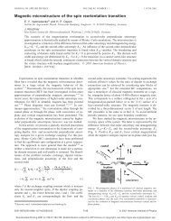
Structure of the multiferroic BaTiO3/Fe(001) interface<br />
Selected Results<br />
H. L. Meyerheim, F. Klimenta, A. Ernst, K. Mohseni, S. Ostanin, M. Fechner, and S. S. Parihar<br />
in cooperation with<br />
I. V. Maznichenko and I. Mertig<br />
Martin-Luther-Universität Halle-Wittenberg, Halle, Germany<br />
A considerable amount of ongoing research<br />
is directly aimed at controlling magnetism<br />
with electric fields and vice versa. One approach<br />
is based on interfacial magneto-electric<br />
coupling via multiferroic interfaces consisting<br />
of a ferroelectric (FE) and a ferromagnetic<br />
(FM) component. Theory has predicted the<br />
possibility of significant changes in the interfacial<br />
magnetization and spin polarization in<br />
a ferromagnet in response to the ferroelectric<br />
polarization state across the interface [1].<br />
In this context, the BaTiO3/Fe(001) interface<br />
represents an archetype system in which<br />
the classical FE film is combined with the FM<br />
electrode in an almost perfect lattice match<br />
(misfit 1.4%). Surprisingly, current knowledge<br />
is limited to theoretical predictions, while<br />
quantitative information on growth, film and<br />
interface structure is not available so far. To<br />
this end we have carried out a combined surface<br />
X-ray diffraction (SXRD) and theoretical<br />
study to elucidate the structural and multiferroic<br />
properties of the BaTiO3/Fe(001) interface,<br />
which go far beyond current knowledge<br />
[2]. Using a KrF (248nm) excimer laser,<br />
BaTiO3 films were grown on the atomically<br />
clean Fe(001) surface by pulsed laser deposition<br />
at room temperature followed by annealing<br />
for 10 min at 600 ◦ C. After this preparation<br />
a c(2×2) superstructure pattern with respect to<br />
the primitive Fe(001) surface unit cell was observed<br />
by low-energy electron diffraction and<br />
surface X-ray diffraction.<br />
The experiments were carried out in situ<br />
in an ultra-high vacuum X-ray diffractometer<br />
using a multilayer X-ray optics focusing Xrays<br />
generated by a rotating anode generator<br />
(Co-Kα radiation, λ=1.79 Å). Fig. 1 shows<br />
the observed (symbols) and calculated (lines)<br />
16<br />
50<br />
0<br />
100<br />
50<br />
0<br />
100<br />
50<br />
|F| (arb. units) |F| (arb. units) |F| (arb. units)100<br />
3 BTO<br />
2 BTO<br />
1 BTO<br />
(1/2 1/2)<br />
(1/2 3/2)<br />
(3/2 3/2)<br />
100<br />
10<br />
100<br />
10<br />
100<br />
10<br />
(1 0)<br />
(1 1)<br />
(2 0)<br />
0<br />
0.0 0.5 1.0 1.5 0.0 0.5 1.0 1.5<br />
qz (rec. latt. units) qz (rec. latt. units)<br />
Fig. 1: Experimental (symbols) and calculated<br />
(lines) structure factor amplitudes along several integer<br />
and superlattice rods for Fe(001) covered by<br />
1, 2 and 3 unit cells of BTO.<br />
structure factor amplitudes for films of 1, 2,<br />
and 3 unit cell(s) thickness (1 BTO, 2 BTO,<br />
3 BTO) along several superstructure (left) and<br />
Fe(001) bulk truncation rods. The parameter<br />
qz corresponds to the momentum transfer normal<br />
to the sample surface. Error bars represent<br />
the standard deviations (1σ). Very good<br />
fits could be achieved quantified by the unweighted<br />
residuum (Ru). Excellent values in<br />
the range of Ru=0.10-0.13 were obtained in<br />
general. The corresponding structure models<br />
are shown in Fig. 2.<br />
All films are terminated by a BaO layer,<br />
while a TiO2 layer is adjacent to the Fe(001)<br />
surface where the bonding is mediated between<br />
the O atoms atop of the Fe atoms. For<br />
the 1 BTO sample of Fig. 2(a) we determine<br />
δ(Ti−O)=0 and δ(Ba−O)=-0.23Å The pa-
Selected Results<br />
=-0.23<br />
= 0.00<br />
=-0.16<br />
= 0.46<br />
= 0.17<br />
= 0.46<br />
[001]<br />
a<br />
2.03<br />
2.08<br />
1.78<br />
1.83<br />
2.39<br />
1.74 2.49 1.74<br />
=-0.06<br />
= 0.06<br />
= 0.06<br />
= 0.36<br />
= 0.14<br />
= 0.30<br />
b c<br />
[110]<br />
2.05<br />
1.72<br />
1.72 2.04 2.00 2.45 1.76<br />
Ba<br />
Fe(1)<br />
O<br />
Ti<br />
Fe(2)<br />
Fig. 2: Model of the BaTiO3/Fe(001) structure. (a)<br />
- (c): side view for films with m=1, 2, and 3 unit<br />
cells of BaTiO3. Red, green, blue and black spheres<br />
correspond to O, Ba, Ti and Fe atoms, respectively.<br />
Experimental distances and vertical displacements<br />
(δ) between oxygen and the Ti (Ba) atoms are given<br />
in Ångstrom units.<br />
rameter δ defines the relative vertical displacement<br />
between the cation relative to the plane<br />
of oxygen atoms. Thus, the TiO2 layer is totally<br />
flat within the experimental uncertainty<br />
∆δ≈0.10 Å. The Ba atom is below the level of<br />
oxygen atoms (δ
Selected Results<br />
Elementary excitations at magnetic surfaces and their spin dependence<br />
Y. Zhang, P. A. Ignatiev, J. Prokop, I. Tudosa, T. R. F. Peixoto, W. X. Tang,<br />
V. S. Stepanyuk, and K. Zakeri Lori<br />
Collective excitations in solids can be well<br />
described by their representative quasiparticles,<br />
i.e. phonons and magnons. Phonons<br />
are collective modes of lattice vibrations and<br />
magnons represent both collective and singleparticle<br />
spin excitations. In a magnetic solid<br />
they coexist and show comparable energies.<br />
The fundamental question in such a case is<br />
the following: How can one distinguish experimentally<br />
between these two different kinds<br />
of excitations? Using the spin degree of freedom<br />
of the electrons in spin-polarized electron<br />
energy loss spectroscopy (SPEELS) experiments,<br />
we demonstrate that the phonons<br />
and magnons can be unambiguously identified.<br />
As an example we show the results of<br />
a high-quality oxygen-passivated Fe(100) surface.<br />
We probe the dispersion relation of all<br />
surface excitations and shed light onto the nature<br />
of each individual excitation. A comparison<br />
between experimental results and theory<br />
clarifies the character of each phonon branch<br />
[1].<br />
A schematic illustration of the scattering geometry<br />
in our SPEELS experiments is given<br />
in the inset of Fig. 1(a). An electron beam<br />
with energy Ei and spin σi is focused onto the<br />
sample surface. The spin of the incident electrons<br />
can be either parallel or antiparallel to<br />
the magnetization direction of the sample. The<br />
angle- and energy-resolved intensity I(θ f , E f )<br />
of back-scattered electrons is recorded and analyzed.<br />
A fraction of the back-scattered electrons<br />
change their energy due to the creation<br />
or annihilation of surface excitations, thus surface<br />
excitations can be observed as peaks in<br />
the intensity spectrum centered exactly at their<br />
excitation energies. An example of such spectra<br />
acquired for different spin directions of incident<br />
electrons is given in Fig. 1(a). Peaks<br />
revealing surface excitations are marked with<br />
arrows and enumerated. Spectra with posi-<br />
18<br />
tive and negative energies ɛ�ω are named as<br />
loss and gain spectra, respectively. This notation<br />
reflects the direction of the energy transfer<br />
during the scattering event. Excitation peaks<br />
in loss and gain spectra are “twinned” in a<br />
sense, that electrons can create certain quasiparticles<br />
losing energy ɛ�ω, and annihilate the<br />
thermally excited ones gaining energy ɛ�ω. The<br />
“twinned” loss and gain peaks are marked with<br />
the same numbers. As a magnon excitation<br />
corresponds to a spin flip in the sample, if<br />
the incoming electron is of minority character<br />
with a spin of -1/2 � then, according to the total<br />
angular moment conservation rule, the outgoing<br />
electron has to be of majority character<br />
with a spin of +1/2 �, after the excitation of a<br />
magnon.<br />
Fig. 1: (a) SPEEL spectra measured on the<br />
O/Fe(001)-p(1×1) surface with the primary energy<br />
4.1 eV and wave vector transfer 0.3 Å −1 . Blue<br />
(I↑) and red (I↓) spectra are obtained with the spin<br />
of incident electrons parallel to that of the majority<br />
and minority electrons in the sample, respectively.<br />
The inset shows the experimental scattering<br />
geometry. (b) The asymmetry curve defined as<br />
A=(I↓ − I↑)/(I↓ + I↑). Insets illustrate the magnon<br />
annihilation and creation processes.
Selected Results<br />
The time reversal process happens for the<br />
incidence of majority electrons, i.e. the annihilation<br />
of a magnon. The creation and annihilation<br />
processes of magnons are sketched in<br />
the inset of Fig. 1(b). A magnon creation peak<br />
in the loss spectrum appears only when incident<br />
electrons are of minority character, while<br />
a magnon annihilation peak in the gain spectrum<br />
is only produced by majority electrons.<br />
This fact would lead to an opposite sign of<br />
spin asymmetry of magnon peaks in gain and<br />
loss regions (see Fig. 1(b)). Since phonons are<br />
spin-independent quasi-particles, they can be<br />
created and annihilated by incident electrons<br />
of both spin characters (meaning the same sign<br />
of spin asymmetry in gain and loss peaks).<br />
Based on this fact one concludes that the excitation<br />
“3” in Fig. 1(a) is a magnon while the<br />
others are phonons.<br />
The intensity spectra recorded for different<br />
wave vectors are presented in Figs. 2(a) and<br />
2(b). Careful fitting of the spectra with a superposition<br />
of Gaussian peaks revealed five excitation<br />
branches which are marked in Figs. 2(c)<br />
and 2(d) with symbols. Phonon branches labeled<br />
“1”, “2”, “4” and “5” are represented by<br />
open symbols, while a magnon branch labeled<br />
“3” is plotted by filled symbols.<br />
To understand the observed phonon modes,<br />
we performed calculations of the harmonic<br />
phonons of the O/Fe(001)-p(1×1) surface by<br />
means of the direct calculations of the force<br />
matrix. Figures 2(c) and 2(d) show the spectral<br />
densities of phonons projected on the oxygen<br />
and the topmost Fe atoms. Based on the theoretical<br />
calculations, we conclude: The phonon<br />
branch “5” with the lowest energy originates<br />
from the acoustical z-polarized transversal oscillations<br />
of the topmost Fe and O layers. It<br />
is the so-called Rayleigh wave of the surface<br />
and has been also observed in He-atom<br />
scattering experiments [2]. In the Fe layer<br />
branch “4” is a longitudinal acoustic phonon<br />
with x-polarization, while in the O layer it is<br />
transversal with z-polarization. Phonon branch<br />
“2” spreading off the ¯Γ-point at the energy of<br />
� 33 meV plotted with squares in Figs. 2(c)<br />
and 2(d) is a z-polarized surface resonance of<br />
the phonons of the Fe slab. Two high-energy<br />
branches at � 50 meV are optical z- transversal<br />
or x- longitudinal phonons localized mostly<br />
at the oxygen atoms.<br />
! " #<br />
#<br />
$ %<br />
Fig. 2: (a) and (b) SPEELS spectra measured for<br />
different in-plane wave vectors. Theoretically calculated<br />
phonon spectral density maps projected on<br />
(c) the oxygen layer and (d) the topmost Fe layer.<br />
Open symbols denote the phonon branches numbered<br />
by “1”, “2”, “4” and “5”; filled symbol denotes<br />
the magnon branch and is numbered by “3”.<br />
The corresponding directions are illustrated in the<br />
inset of (c).<br />
In summary, we have shown that the<br />
magnon and phonon excitations on relatively<br />
complex magnetic surfaces can be measured<br />
and unambiguously distinguished based on<br />
their different spin nature. Our results demonstrate<br />
a promising application of SPEELS in<br />
the study of magnons and phonons and the<br />
their possible coupling.<br />
References<br />
[1] Y. Zhang et al., Phys. Rev. Lett. 106, 127201<br />
(2011).<br />
[2] G. Fahsold et al., Appl. Surf. Sci. 137, 224<br />
(1999).<br />
&<br />
%<br />
19
Selected Results<br />
Investigation of unoccupied quantum well states in Co/Cu(001)<br />
C.-T. Chiang, A. Winkelmann, J. Henk, and P. Yu<br />
Unoccupied electronic states determine the<br />
reaction of electrons in a crystal when it is excited<br />
by intense light from a high-power laser.<br />
An unoccupied state can be analyzed by first<br />
populating it with a photoelectron from an occupied<br />
intial state and then probing this excited<br />
state with an additional photon in the<br />
method of two-photon-photoemission (2PPE).<br />
The spin of the excited electrons, which is related<br />
to their magnetic moment, is of great interest<br />
in ferromagnets, since optical excitation<br />
by lasers can be used to influence the magnetization<br />
of a sample. Moreover, the electron spin<br />
is coupled to the orbital motion, a mechanism<br />
which for instance influences the preferential<br />
orientation of the magnetization in crystals.<br />
In magnetic systems, the optical transition<br />
probability is also influenced by the spin-orbit<br />
coupling and shows changes in x-ray absorption<br />
[1] and photoemission intensity [2] upon<br />
magnetization reversal. This effect is called<br />
magnetic dichroism. By a unique combination<br />
of 2PPE with magnetic dichroic methods, we<br />
have access to spin-orbit coupling in the unoccupied<br />
electronic states, which helps us to<br />
obtain a more complete picture of the spindependent<br />
band stucture and we gain insights<br />
into the optically triggered dynamics on the<br />
femtosecond time scale. 2PPE can therefore be<br />
viewed as a very useful tool which is complementary<br />
to valence band photoemission for investigation<br />
of the unoccupied electronic states.<br />
As a special type of unoccupied states, we<br />
have systematically investigated quantum well<br />
(QW) states which are formed due to the confinement<br />
of electrons in ultrathin ferromagnetic<br />
cobalt films deposited on Cu(001). By<br />
using frequency converted laser pulses with<br />
photon energies of 3.1 eV and 6.0 eV, we can<br />
reveal the presence of unoccupied QW states<br />
by a comparison of 2PPE with one-photon<br />
photoemission (1PPE) experiments. In Fig.<br />
1(a), the features of the QW states in the 2PPE<br />
20<br />
spectra are identified by their characteristic dependence<br />
on the cobalt film thickness. The<br />
first QW state appears at 4.7 eV at 3 monolayers<br />
(ML) Co and disperses up to 5.5 eV at<br />
8 ML. Starting from 10 ML, we can observe<br />
the feature of the second QW state emerging<br />
at 4.8 eV and its upward shift in energy. In<br />
the 1PPE spectra in Fig. 1(b), the features of<br />
the unoccupied QW states are missing because<br />
they are not involved in the 1PPE process. The<br />
cobalt thickness dependence of the QW states<br />
Fig. 1: Cobalt thickness dependent (a) two-photon<br />
photoemission with hν = 3.1 eV and (b) one-photon<br />
photoemission with hν = 6.0 eV. The incident light<br />
is p-polarized. Unoccupied quantum well states are<br />
observed in the 2PPE spectra, e.g. at the position<br />
marked by the dashed circle for 6ML Co (a) [3].
Selected Results<br />
agrees well with our theoretical calculations<br />
[4] as well as with previous inverse photoemission<br />
experiments.<br />
In addition, we observe increased intensity<br />
due to the occupied cobalt d-bands near the<br />
Fermi level of the 1PPE and 2PPE spectra in<br />
Fig. 1. Furthermore, a periodic modulation of<br />
the photoemission intensity as a function of the<br />
cobalt thickness deposited is seen. This intensity<br />
oscillation can be associated with the periodic<br />
change of the surface morphology during<br />
the layer-by-layer growth of the ultrathin films<br />
after 2 ML of Co are deposited.<br />
To examine the magnetic dichroic signal in<br />
2PPE, we focussed on the quantum well state<br />
in 6 ML cobalt films which appears at 5.4 eV<br />
final state energy in the 2PPE spectra (dashedcircle<br />
in Fig. 1(a). In these measurements, the<br />
sample magnetization was aligned in the optical<br />
plane and parallel to [110] crystal directions.<br />
The incident linear polarization of the<br />
laser light was varied continuously and is represented<br />
by the angle α of the electric field vector<br />
relative to the optical plane. As shown in<br />
Fig. 2(a), we observed a strong dependence of<br />
the 2PPE intensity as a function of the angle α<br />
and we also see clear intensity changes upon<br />
magnetization reversal of the sample. The<br />
magnetic dichroic effect is represented by the<br />
relative intensity asymmetry between opposite<br />
magnetization directions, AMLD, which is defined<br />
in Fig. 2(b). We find that the dichroic effect<br />
appears when the incident light is neither<br />
perfectly p- nor s-polarized (α � 0 ◦ , ±90 ◦ ).<br />
Moreover, the dichroic signal changes its sign<br />
when the sign of angle α is reversed and it<br />
reaches its maximum around ±75 ◦ .<br />
We further compared our experimental results<br />
with theoretical photoemission calculations.<br />
In the calculations, the spin-orbit<br />
coupling in the cobalt electronic structure is<br />
treated by using the Dirac equation in a layer-<br />
KKR method [4]. The theoretical photoemission<br />
signal in Fig. 2(b) is calculated from QW<br />
states which are assumed to be transiently populated<br />
by excited electrons. We see very good<br />
agreement of the theory with the experiments,<br />
indicating that we capture the main physics of<br />
Fig. 2: (a) Magnetization dependent two-photon<br />
photoemission as a function of incident polarization<br />
of light at around 5.4 eV for 6 ML cobalt films<br />
(chosen region in Fig. 1(a) [4]. (b) Photoemission<br />
intensity asymmetry from experiments compared<br />
to theoretical calculations.<br />
the effects observed. Specifically, we can identify<br />
the weak but measurable spin-orbit coupling<br />
in the unoccupied cobalt quantum well<br />
states as the origin of the magnetic dichroism<br />
we observed.<br />
References<br />
[1] G. Schütz, W. Wagner, W. Wilhelm, P. Kienle,<br />
R. Zeller, R. Frahm, and G. Materlik, Phys. Rev.<br />
Lett. 58, 737 (1987).<br />
[2] L. Baumgarten, C. M. Schneider, H. Petersen, F.<br />
Schäfers, and J. Kirschner, Phys. Rev. Lett. 65,<br />
492 (1990).<br />
[3] C.-T. Chiang, A. Winkelmann, P. Yu, and J.<br />
Kirschner, Phys. Rev. Lett. 103, 077601 (2009).<br />
[4] C.-T. Chiang, A. Winkelmann, P. Yu, J.<br />
Kirschner, and J. Henk, Phys. Rev. B 81, 115130<br />
(2010).<br />
21
Surface stress change upon condensation of xenon<br />
Condensation of a gas on a cold surface is a<br />
phenomenon which is well known to us from<br />
every day experience. The formation of a layer<br />
of humidity on a bathroom mirror when taking<br />
a hot shower or the fogging of the inner<br />
side of the windscreen of a car, induced by<br />
our breath, when starting off on a cold winter<br />
morning are examples, where moisture condenses<br />
on a cold surface. These observations<br />
already reveal important aspects of the underlying<br />
physics: Condensation requires a cold<br />
surface and the interaction between the adsorbed<br />
species (water) and the substrate surface<br />
(glass) is fairly weak, as the condensed<br />
layer is easily wiped away.<br />
Research on condensation is of significant<br />
interest in surface physics and chemistry [1].<br />
Here, the formation of a weak bond between<br />
adsorbate and surface, known as physisorption,<br />
is distinguished from chemisorption.<br />
There, a strong chemical bond develops<br />
between adsorbate and surface atoms, a process<br />
which takes place for example upon oxidation<br />
(rusting) of steels and tarnishing of silver.<br />
But does physisorption also impact the<br />
properties of the surface? Our experiments on<br />
a prototypical physisorption system, the condensation<br />
of the rare gas xenon on a cold Pt<br />
surface [2, 3] reveal that this is indeed the case.<br />
To elucidate this question we use a recently<br />
developed liquid helium cooled sample manipulator<br />
to measure Xe-induced surface stress<br />
change upon condensation on Pt(111) at 30 K<br />
[4]. Figure 1 presents the results in conjunction<br />
with low energy electron diffraction<br />
(LEED) images taken at the clean and Xecovered<br />
Pt(111) surface. We find a surprisingly<br />
large compressive surface stress change<br />
of −2.2 N/m upon exposure of the clean Pt<br />
crystal to a Xe partial pressure of 1×10 −7 mbar<br />
for 320 s.<br />
The LEED images reveal a pronounced<br />
change of the diffraction pattern induced by Xe<br />
22<br />
D. Sander and J. Premper<br />
Selected Results<br />
Fig. 1: Stress measurements and electron diffraction<br />
images during the the condensation of Xe on<br />
Pt(111) at 30 K. The stress curve (red, left scale)<br />
indicates a sizeable compressive stress change of<br />
−2.2 N/m upon exposure of the clean Pt(111) surface<br />
to Xe at a partial pressure (blue, right scale)<br />
of 1 × 10 −7 mbar for 320 s. The top row shows<br />
LEED images at 87 eV taken before and after Xe<br />
exposure. Upon Xe exposure an area of blurred<br />
diffracted intensity is found within the Pt first order<br />
diffraction peaks labelled (1,0) and (0,1).<br />
exposure. Prior to exposure a pattern indicative<br />
of clean Pt(111) is observed, with distinct<br />
and strong diffraction spots. This is shown in<br />
the top row of Fig. 1, left image, where some<br />
diffractions spots are identified. After exposure,<br />
these spot intensities are diminished, see<br />
the labels in the right image. An area with a<br />
blurred intensity distribution is now observed<br />
at the inner region. This LEED pattern suggests<br />
that Xe has condensed on the Pt(111)<br />
crystal, forming a not well ordered structure<br />
on top of the surface at 30 K. Slight annealing<br />
of this structure to 80 K induces the formation<br />
of an ordered Xe- √ 3 × √ 3 surface structure.<br />
The surface stress change of order −2.2 N/m<br />
appears to be remarkably large for a phy-
Selected Results<br />
sisorbed system. This assessment is based<br />
on surface stress measurements on Pt(111) for<br />
chemisorbed oxygen, where a saturation coverage<br />
of O induces a compressive stress of<br />
−2.2 N/m [5]. Here, a strong chemical bond<br />
O–Pt with a binding energy of 5.5 eV is formed<br />
[5]. It contrasts with the much lower adsorption<br />
energy of 0.29 eV per atom for Xe on<br />
Pt(111) [1]. This comparison leads us to the<br />
first important result of this study which indicates<br />
that the strength of the adsorbate bond is<br />
not necessarily a valid indicator for the magnitude<br />
of the resulting adsorbate-induced surface<br />
stress change.<br />
This comes as a surprise, as one might have<br />
speculated that a weak adsorbate-substrate interaction,<br />
as indicated by a minute binding energy,<br />
should be linked to a small distortion of<br />
the electronic structure of the substrate surface<br />
region upon, and consequently a negligible<br />
change of surface stress should result. This<br />
line of thought fails to describe the comparably<br />
strong surface stress change induced by Xe.<br />
An important point in this respect is the<br />
change of the electronic charge density at the<br />
Pt(111) surface upon Xe-condensation. This<br />
has been calculated [3], and the result is shown<br />
in Fig. 2. The plot reveals that the electronic<br />
charge density changes at both, the Xe atom<br />
and the Pt surface atom due to the adsorption<br />
of Xe on the surface. Electronic charge is reduced<br />
at the Xe atom, it is enhanced between<br />
Xe and the surface, and it is depleted within the<br />
Pt surface layer. Although the binding energy<br />
of Xe is low, there is a substantial modification<br />
of the electronic structure of the substrate.<br />
The impact of this charge redistribution on<br />
surface stress has not been addressed yet. Future<br />
experimental and theoretical endeavors<br />
are called for to elucidate the electronic origin<br />
of rare gas induced surface stress changes. It is<br />
tempting to speculate that the Pauli exclusion<br />
principle, which comes into play when closed<br />
shell electron clouds of neighboring rare gas<br />
atoms start to interact, might be a further factor<br />
contributing to the compressive surface stress<br />
change.<br />
Our measurements of rare gas induced sur-<br />
3.07 A<br />
Xe/Pt<br />
Xe<br />
Pt<br />
�n � n � n � n �n<br />
Fig. 2: Plot of the calculated change of electronic<br />
charge density ∆n for Xe adsorption at a height of<br />
3.07 Å on top of a Pt(111) surface atom. The blue<br />
color indicates a decrease of electronic charge density<br />
around the Xe atom, whereas the charge density<br />
is enhanced between Xe and Pt. This indicates<br />
the formation of a surface dipole, where the positive<br />
charge is located near the Xe atom, and the<br />
negative close to the surface. Note that within the<br />
topmost Pt surface layer a reduction of charge density<br />
is calculated. Adopted from [3].<br />
face stress change provide novel and first experimental<br />
insights into a largely unexplored<br />
field of surface science, where we strive for<br />
an improved understanding of forces acting in<br />
surface layers.<br />
References<br />
Xe<br />
[1] L. W. Bruch, R. D. Diehl, and J. A. Venables, Rev.<br />
Mod. Phys. 79, 1381 (2007).<br />
[2] J. E. Müller, Phys. Rev. Lett. 65, 3021 (1990);<br />
Appl. Phys. A 87, 433 (2007).<br />
[3] J. L. F. DaSilva, C. Stampfl, and M. Scheffler,<br />
Phys. Rev. Lett. 90, 066104 (2003).<br />
[4] J. Premper, Diploma thesis, Martin Luther University<br />
Halle-Wittenberg, 2010.<br />
[5] Z. Tian, D. Sander, N. N. Negulyaev, V. S. Stepanyuk,<br />
and J. Kirschner, Phys. Rev. B 81, 113407<br />
(2010).<br />
Pt<br />
23
Selected Results<br />
Quantum well states and oscillatory magnetic anisotropy in thin Fe films<br />
U. Bauer, M. Dabrowski, J. Li, Y. Z. Wu, and M. Przybylski<br />
in cooperation with<br />
M. Cinal<br />
<strong>Institut</strong>e of Physical Chemistry of the Polish Academy of Sciences, Warsaw, Poland<br />
Magnetic anisotropy is one of the key<br />
properties of ferromagnetic films (FM) and<br />
nanostructures and is of particular importance<br />
for their application in magnetic recording<br />
and spintronics. The magnetocrystalline<br />
anisotropy is caused by spin-orbit coupling<br />
of electrons, which can be interpreted as a<br />
coupling between the spin of a moving electron<br />
and the relativistic effect of the electric<br />
field created by all nuclei and other electrons<br />
present in the system. The magnetocrystalline<br />
anisotropy energy (MAE) results<br />
from the anisotropy of the spin-orbit coupling,<br />
i.e. it is the difference of the total energies obtained<br />
including the spin-orbit coupling term<br />
with the magnetization pointing in two different<br />
directions.<br />
Since spin-orbit coupling is small, it can be<br />
treated as a perturbation. The resulting correction<br />
to the total energy of the system becomes<br />
relevant only if the energy difference between<br />
the unoccupied and occupied states is small,<br />
and thus only the pairs of the states of energies<br />
close to each other can contribute significantly<br />
to MAE.<br />
In a thin film electrons can move back and<br />
forth between the upper and lower surface.<br />
They may form standing waves if the wavelength<br />
of the electron waves fits into the thickness<br />
of the film. Such standing waves represent<br />
states called quantum well states (QWS),<br />
which can be occupied by electrons or remain<br />
unoccupied. With increasing film thickness,<br />
the energies of these pairs move. At specific<br />
thicknesses (tn = t0 + nL, n=1,2,..), there exists<br />
a pair of occupied and unoccupied states<br />
for which the energies are very close to each<br />
other, and thus they contribute significantly to<br />
MAE. The oscillation period L is determined<br />
24<br />
Fig. 1: Schematics of Fe wedge on stepped surface<br />
of Ag(001) with easy magnetization axis (blue<br />
arrows) oriented parallel or perpendicular to the<br />
steps. Red arrows represent incoming and outgoing<br />
laser beam. Representative hysteresis loops for longitudinal<br />
MOKE measurements for the easy magnetization<br />
axis oriented either parallel (left panel)<br />
or perpendicular (right panel) to the steps are also<br />
shown. ∆S P denotes additional polar MOKE signal<br />
due to tilting of the easy axis relative to the sample<br />
plane by angle δ, not discussed here.<br />
by the wavelength of the electron waves.<br />
For thin films grown on single-crystalline<br />
substrates, magnetic anisotropy reflects the<br />
symmetry of the crystal surface. In particular,<br />
films grown on (001) surfaces exhibit a<br />
so-called fourfold anisotropy. Small changes<br />
of magnetic anisotropy can be easily followed<br />
if the fourfold symmetry is lowered by growing<br />
FM films on stepped surfaces. The lower<br />
symmetry has the consequence that the easy<br />
magnetization axes of the fourfold anisotropy<br />
are not equivalent any more. In case the steps<br />
are oriented along one of the easy axes of the<br />
fourfold anisotropy of a FM film, one of them<br />
becomes the easy magnetization axis and the<br />
other the intermediate magnetization axis.
Selected Results<br />
In order to orient the magnetization along<br />
the intermediate axis, it is necessary to apply<br />
a small magnetic field. As a result, so-called<br />
split hysteresis loops can be measured, which<br />
are characterized by a shift field (Hs) being<br />
defined as half of the distance between two<br />
constituent loops. The more the magnetization<br />
prefers an orientation along the easy-axis<br />
(i.e. the larger the anisotropy, the larger Hs).<br />
Therefore, Hs can be taken as a measure of the<br />
anisotropy modification introduced by the substrate<br />
steps (Fig. 1). Positive or negative Hs<br />
refers to the situation where the easy magnetization<br />
axis is oriented along or perpendicular<br />
to the steps, respectively [1].<br />
The experiments were performed for Fe<br />
films grown on Ag(1,1,10) and Ag(1,1,6).<br />
These are vicinal surfaces of Ag(001) with an<br />
average terrace width of 4.5 and 2.5 atomic<br />
distances, respectively. Magnetic hysteresis<br />
loops were probed by in situ longitudinal magnetooptical<br />
Kerr effect (MOKE) with a laser<br />
diode of wavelength 670 nm and beam diameter<br />
Circular dichroism in double photoemission<br />
If the absorption of light in matter depends<br />
on the helicity one calls this circular dichroism.<br />
This absorption dependence manifests itself<br />
also in the kinetic energy spectra of emitted<br />
electrons. An example is core-level (e.g.<br />
2p or 3p) photoemission on magnetic materials<br />
which provides magnetic contrast. Our<br />
recent activities are devoted to the study of<br />
electron pair emission upon photon absorption<br />
termed also double photoemission (DPE)<br />
[1, 2]. In particular, we focussed on an energy<br />
window which includes the emission of a 3p<br />
photoelectron and the related Auger electron<br />
[2]. This type of labeling follows from a single<br />
electron notation. On the other hand coincidence<br />
experiments emphasize the property of<br />
the pair rather than those of the individual electrons.<br />
Therefore the question arises whether<br />
it is possible to observe dichroism for pairs<br />
while the single electron spectra display no<br />
dichroic effect. In order to address this point<br />
we performed a DPE experiment on a Cu(001)<br />
surface. A schematic view of the instrument<br />
and geometry employed is shown in Fig. 1<br />
[2, 3]. Two hemispherical electron energy analyzers<br />
were used to detect two outgoing electrons<br />
in coincidence. The kinetic energies are<br />
given by Ele f t and Eright, respectively. The<br />
BESSY II storage ring served as light source<br />
and we selected a photon energy of hν=125 eV<br />
of circular polarized light. The different helicities<br />
will be labeled as σ + and σ − , respectively.<br />
With this choice of the photon energy and setting<br />
of the analyzers it is possible to detect the<br />
3p photoelectron together with the resulting<br />
Auger electron. In the conventional description<br />
of Auger emission it is assumed that this<br />
occurs in a subsequent step following the photoelectron<br />
emission. We have demonstrated<br />
previously that this picture is incorrect at least<br />
for a Cu sample [2]. This means that the emitted<br />
pair is a single entity rather than two individual<br />
electrons. This statement was based<br />
26<br />
Z. Wei, R. S. Dhaka, and F. O. Schumann<br />
Selected Results<br />
Fig. 1: Schematic view of the coincidence experiment.<br />
Circularly polarized light impinges onto the<br />
Cu(001) sample in grazing incidence. Electrons<br />
emitted within the gray emission cones are detected<br />
by two hemispherical analyzers. A coincidence circuit<br />
ensures the detection of pairs only.<br />
on the observed energy distributions. An additional<br />
proof would consist in observing a circular<br />
dichroic effect in the electron pair emission<br />
while the single electron spectra do not<br />
show circular dichroism. In Fig. 2 we display<br />
the important result. Panel (a) shows the 2D<br />
energy distribution for the sum of both helicities<br />
(σ + +σ − ), while in panel (b) the difference<br />
(σ + -σ − ) is shown. It is apparent that the 2D<br />
energy spectrum in panel (a) has two localized<br />
regions where the intensity is maximal. Those<br />
regions are marked with A and B with the energy<br />
coordinates (45 eV, 57 eV) and (57 eV,<br />
45 eV), respectively. These energies can be<br />
easily identified as the photoelectron at 45 eV<br />
while 57 eV is the kinetic energy of the Auger<br />
electron. The dashed diagonal line through the<br />
intensity pockets marks a line of constant sum<br />
energy Esum = Ele f t + Eright. Along this line,<br />
but outside the regions A and B, the intensity<br />
is not zero but has a finite value. This can only
Selected Results<br />
Fig. 2: In (a) we display the 2D energy distribution<br />
for the sum of both helicities (σ + +σ − ). In (b)<br />
we show the difference (σ + -σ − ) spectrum. The energy<br />
regions A and B mark those positions where<br />
a 3p photoelectron and Auger electron is detected<br />
in coincidence. At these positions the difference is<br />
largest. It amounts to ± 12 % if we compute the<br />
ratio of the difference to the sum.<br />
be understood if we consider the electron pair<br />
as a single entity [2]. The difference spectrum<br />
(σ + -σ − ) is essentially constant over the whole<br />
2D energy window except near the regions A<br />
and B. Near region A the difference is positive<br />
while at region B it is negative, the integral of<br />
the difference spectrum is zero as expected for<br />
a dichroic effect.<br />
In order to proof that the dichroic effect observed<br />
in Fig. 2 (b) is a genuine effect of a<br />
pair, one needs to show that the single electron<br />
spectra display no dichroism. These were<br />
obtained without the coincidence logic. As an<br />
example we show in Fig. 3 (a) such a spectrum.<br />
The spectra cover the photoelectron and<br />
Auger electron with the energy positions labeled.<br />
The red spectrum has been measured<br />
with σ + while the blue spectrum was measured<br />
Fig. 3: In a) we display helicity dependent single<br />
electron spectra which include the Auger and 3p<br />
photoelectron. In b) we plot the difference curve<br />
which is close to zero. Calculating the ratio of the<br />
difference to the sum gives a value below 3 %.<br />
with σ − . Both spectra are essentially identical<br />
as the difference spectrum displayed in panel<br />
b) demonstrates. In particular, there is no difference<br />
intensity at the energy positions of the<br />
single electron peaks. We conclude that the<br />
dichroic effect seen in Fig. 2 (b) is not due<br />
to dichroism in the single electron spectra, but<br />
is a property of the pair. This is additional evidence<br />
that the Auger emission proceeds in a<br />
single step upon photon absorption by the core<br />
level.<br />
References<br />
[1] F.O. Schumann, C. Winkler, and J. Kirschner,<br />
physica status solidi (b) 246, 1483 (2009).<br />
[2] G.A. van Riessen, Z. Wei, R.S. Dhaka, C. Winkler,<br />
F.O. Schumann and J. Kirschner, J. Phys.:<br />
Condens. Matter 22, 092201 (2010).<br />
[3] G.A. van Riessen, F.O. Schumann, M. Birke, C.<br />
Winkler, and J. Kirschner, J. Phys. Cond. Matter<br />
20, 442001 (2008).<br />
27
Selected Results<br />
Spin resolved photoelectron microscopy using a two-dimensional<br />
spin-polarizing electron mirror<br />
C. Tusche, M. Ellguth, A. A. Ünal, C.-T. Chiang, A. Winkelmann, A. Krasyuk, and J. Kirschner<br />
in cooperation with<br />
M. Hahn and G. Schönhense<br />
Johannes-Gutenberg-Universität Mainz, Mainz, Germany<br />
Electrons in a solid state system are<br />
in principle characterized by their energy-,<br />
momentum-, and spin degrees of freedom. In<br />
particular, the spin of the electron gives rise<br />
to many fundamental phenomena observed in<br />
solid state physics, like magnetism and electron<br />
correlation. However, while energy and<br />
momentum are readily accessible in a photoemission<br />
experiment, it takes considerable effort<br />
to measure the spin degree of freedom of<br />
the electron.<br />
As electrons cannot be separated by their<br />
spin (“up” or “down”) in a Stern-Gerlach type<br />
experiment, an electron spin detector involves<br />
scattering at a suitable target where a measurable<br />
quantity, e. g. the scattering cross section,<br />
shows an asymmetry with respect to the spin.<br />
Setups typically employed are the Mott- or<br />
SP-LEED detectors [1]. These are characterized<br />
by a fairly low efficiency, due to an overall<br />
low reflectivity or a low asymmetry function,<br />
and the restriction to measure only one<br />
data point at a time. This, in particular, is<br />
a major limitation when using state-of-the-art<br />
electron spectrometers with multichannel detection<br />
and electron microscopy imaging techniques.<br />
There, due to the large number of data<br />
points, spin-resolved measurements are practically<br />
impossible with existing single-channel<br />
spin detectors.<br />
To access the local electron spin polarization<br />
in images recorded by a photoelectron<br />
emission microscope (PEEM), we developed a<br />
new two-dimensional (2D) spin filter. The 2D<br />
spin filter, similar to the SP-LEED detector, is<br />
based on the spin dependent reflectivity of low<br />
energy electrons at a single crystal target due<br />
to spin-orbit coupling [2]. Here we have cho-<br />
28<br />
sen a W(100) crystal due to its reliable preparation<br />
procedure. In the 2D spin filter, scattering<br />
takes place in the (00)-LEED spot, which<br />
is unique among all LEED reflections in that<br />
the momentum transfer vector is oriented normal<br />
to the target surface. This geometry allows<br />
us to encode the additional information associated<br />
with the x and y coordinate of the PEEM<br />
image into the angle of incidence of electrons<br />
scattered at the W(100) target. Like for a mirror,<br />
this angle is conserved after reflection even<br />
when a small energy spread of the incoming<br />
beam is allowed [3].<br />
source image<br />
retarding lens<br />
spin−filtered image<br />
W(100) crystal<br />
direct image<br />
for retracted target<br />
Fig. 1: Scattering geometry at the W(100) crystal.<br />
Scattering takes place under parallel beam conditions,<br />
preserving the spatial information of the<br />
source image. The spin-integrated image is obtained<br />
by retracting the W(100) crystal.<br />
As outlined in Fig. 1, the W(100) crystal is<br />
mounted at 45 ◦ with respect to the incoming<br />
beam. The transformation of the PEEM image<br />
into a parallel beam and vice versa is accomplished<br />
by two identical electrostatic retarding<br />
lenses. These lenses are also used to adjust the<br />
kinetic energy of the electrons to the optimum<br />
working point.<br />
As a first proof of principle we recorded<br />
spin-resolved PEEM images of the magnetic
Selected Results<br />
a)<br />
M ±<br />
b)<br />
[010]<br />
[001]<br />
25°<br />
p<br />
intensity (arb. u.)<br />
1.4<br />
1.2<br />
1<br />
intensity (arb. u.)<br />
1.6<br />
1.4<br />
1.2<br />
1.0<br />
0.8<br />
line profile<br />
fit<br />
0 1 2 3 4<br />
distance (µm)<br />
Fig. 2: (a) Spin-filtered PEEM image of magnetic<br />
domains of an 8 ML Co film observed after the<br />
electron beam was scattered at the W(100) crystal.<br />
(b) A high magnification image of the area marked<br />
by the circle in (a). The inset in (b) shows an intensity<br />
profile across the domain wall as indicated by<br />
the line.<br />
domain structure of ultrathin Co films grown<br />
on a Cu(100) surface, a well characterized prototypical<br />
system. In particular, from other experiments,<br />
a 40-50% spin polarization of electrons<br />
emitted in two-photon-photoemission<br />
(2PPE) is known.<br />
As the most important result, the pattern<br />
of vertically aligned magnetic domains in the<br />
Co film can be directly observed as a blackwhite<br />
contrast when the electrons are scattered<br />
with Ekin = 27 eV at the target. In the 2PPE-<br />
PEEM image shown in Fig. 2(a), the grey scale<br />
directly corresponds to measured intensities<br />
from the CCD camera. Remarkably, the image<br />
in Fig. 2(a) was integrated over a time of<br />
only 120 s. This comparably short time is the<br />
result of the simultaneous measurement of all<br />
image pixels within one single exposure.<br />
Figure 2(b) shows a high magnification image<br />
of the magnetic domain boundary. From<br />
the line profile (see inset) across the domain<br />
wall we observe an intensity variation of 46%.<br />
With the known spin polarization of the photoelectrons<br />
this translates into a spin sensitivity<br />
(i. e. the asymmetry expected for a 100%<br />
polarized beam) of S = 42 ± 5%. The width<br />
of the domain wall derived from the profile is<br />
500 ± 30 nm. This value is about 20% larger<br />
than values <strong>report</strong>ed in literature for films of<br />
comparable thickness [4]. It is therefore reasonable<br />
to conclude that the instrumental image<br />
resolution is better than 300 nm, corresponding<br />
to a total of 3800 independent pixels<br />
in the image. This is an important result, as<br />
the efficiency of the spin detector, defined by<br />
the rate at which data points are collected, is<br />
directly proportional to the number of parallel<br />
detected pixels. A comparison with the typical<br />
mosaic spread of a high quality tungsten crystal<br />
shows that the observable number of independent<br />
pixels is primarily limited by the quality<br />
of the crystal, through angular broadening<br />
of the reflected beam [3].<br />
While we demonstrated spin filtering of<br />
PEEM images, the same setup can be used<br />
for the spin analysis of any 2D electron distribution.<br />
In particular, applications in multichannel<br />
electron spectrometers, or the spinresolved<br />
measurement of 2D electron momentum<br />
images are possible.<br />
References<br />
[1] D. Pierce, R. Celotta, M. Kelley, and J. Unguris,<br />
Nucl. Instrum. Methods Phys. Res. A 266, 550<br />
(1988)<br />
[2] J. Kirschner and R. Feder, Phys. Rev. Lett. 42,<br />
1008 (1979)<br />
[3] C. Tusche, M. Ellguth, A. A. Ünal, C.-T. Chiang,<br />
A. Winkelmann, A. Krasyuk, M. Hahn, G.<br />
Schönhense, and J. Kirschner, Appl. Phys. Lett.<br />
99, 032505 (2011)<br />
[4] A. Berger and H. P. Oepen, Phys. Rev. B 45,<br />
12596 (1992)<br />
29
Selected Results<br />
Domain walls in ferroelectric and multiferroic materials – microstructure<br />
and impact on material properties<br />
M. Alexe, Y. S. Kim, I. Vrejoiu, and D. Hesse<br />
in cooperation with<br />
H. Han and S. Baik<br />
Pohang University of Science and Technology, Pohang, Korea<br />
and<br />
W. Lee<br />
Korea Research <strong>Institut</strong>e of Standards and Science, Daejeon, Korea<br />
Domain walls in ferroic (ferroelectric, ferromagnetic<br />
or ferroelastic) materials significantly<br />
contribute to the properties of the latter,<br />
because microstructure and mobility of these<br />
walls largely determine the switching properties.<br />
Switching between different states is a<br />
fundamental process which occurs in many applications<br />
of ferroic materials. 180 ◦ domain<br />
boundaries in ferroelectric materials, e.g., determine<br />
the switching properties of ferroelectric<br />
random access memories. In case of multiferroic<br />
materials, i.e. materials involving at<br />
least two ferroic order parameters simultaneously,<br />
even switching between, e.g., four different<br />
memory states may occur. Microstructure,<br />
mobility, and other properties of domain<br />
walls are thus presently under investigation,<br />
particularly on the nanoscale, because the increasing<br />
demands for a high memory density<br />
result in a downsizing of the memory elements<br />
into the nanoscale range.<br />
In micron-size ferroelectric capacitors,<br />
switching follows the well-known<br />
Kolmogorov-Avrami-Ishibashi (KAI) kinetics.<br />
Our experiments on Pt/Pb(Zr,Ti)O3/Pt<br />
nanocapacitors showed, however, that the KAI<br />
model is not applicable in nanocapacitors [1].<br />
An epitaxial Pb(Zr0.2Ti0.8)O3 (PZT) thin film<br />
of 35 nm thickness was deposited onto an<br />
epitaxial Pt layer on a MgO(100) single<br />
30<br />
and<br />
C.-L. Jia and K. W. Urban<br />
Forschungszentrum Jülich, Jülich, Germany<br />
crystal substrate by pulsed laser deposition<br />
(PLD). Nanosize Pt top electrodes were<br />
deposited by e-beam evaporation through an<br />
anodic alumina stencil mask with a pore size<br />
of 70 nm. To observe switching dynamics, the<br />
method described by Gruverman et al. was<br />
used using piezoresponse force microscopy<br />
(PFM) [2].<br />
Fig. 1: (a) PFM phase, (b) PFM amplitude images,<br />
and (c) schematical cross-sectional domain structures<br />
developing at different pulse widths between<br />
200 ns and 1 s under an applied voltage of +2 V [1].<br />
Figure 1 shows PFM images of the domain<br />
configuration developed at different pulse<br />
widths between 200 ns and 1 s. Polarization<br />
switching for most of the nanoscale capacitors<br />
typically proceeds as expected via nucleation<br />
and subsequent lateral domain growth.<br />
But unlike the case of micron-scale capacitors,<br />
in which many nuclei occur at different<br />
places, here there is always only one nucleus,<br />
which is always generated at the same
Selected Results<br />
edge of the capacitor. Based on the experimental<br />
findings, a new mathematical switching<br />
model of non-KAI type was developed that<br />
is in very good agreement with the experimental<br />
data [1]. The nucleation of a single<br />
180 ◦ domain at the capacitor edge, its rapid<br />
spread towards the counterelectrode, and the<br />
subsequent, slower lateral movement of the<br />
180 ◦ domain boundary (Fig. 1(c)) constitute<br />
the physical base of this model. The different<br />
mobilities of the charged, head-headcoupled,<br />
bottom part and the non-charged,<br />
head-tail-coupled, lateral parts of the parabolic<br />
domain boundary (Fig. 1(c), second from left)<br />
can be explained on the base of the significantly<br />
different atomic-scale microstructure of<br />
charged and non-charged 180 ◦ domain boundaries<br />
in PZT. The latter was analyzed using<br />
the method of negative-spherical-abberationcoefficient<br />
imaging in high-resolution transmission<br />
electron microscopy (HRTEM) [3].<br />
Fig. 2: Part of a processed cross section HRTEM<br />
image of the bottom of a ferroelectric 180 ◦ boundary<br />
in a PZT layer close to the substrate interface.<br />
Image taken with negative coefficient of spherical<br />
abberation in an abberation-corrected TEM at FZ<br />
Jülich. The image was processed to visualize the<br />
magnitude and direction of the electric dipole in<br />
each unit cell and shows the continuous rotation of<br />
the dipoles in a roughly triangular region [4].<br />
Applying the same method, an even more<br />
interesting finding has recently been made:<br />
According to textbook knowledge, the polarisation<br />
vector in tetragonal PZT can have only<br />
six specific directions in space. Different from<br />
the magnetization vector which can continuously<br />
rotate, no such rotation is allowed for the<br />
ferroelectric polarization due to the very large<br />
related electrostrictive energy. However, as we<br />
found, in a nanosize region of a PLD-grown<br />
PZT layer close to its interface with the substrate,<br />
a continuous rotation of the polarization<br />
vector occurs, obviously due to the influence<br />
of the depolarizing field [4]. Figure 2 shows a<br />
correspondingly processed HRTEM image of<br />
the nanoregion, displaying the continuous rotation<br />
of the dipoles.<br />
Fig. 3: Photocurrent-voltage characteristics of a<br />
BiFeO3 single crystal obtained by successively<br />
contacting three tips A, B, C (photo in the inset)<br />
of a multicantilever AFM chip [5].<br />
The impact of the ferroelectric 71 ◦ and 109 ◦<br />
domain boundaries in multiferroic BiFeO3 on<br />
the unconventional photovoltaic properties of<br />
this material are presently under intensive discussion.<br />
We recently studied the anomalous<br />
photovoltaic effect of self-grown BiFeO3<br />
single crystals applying photoelectric atomic<br />
force microscopy and PFM, and we were able<br />
to show that a nanoscale top electrode is able<br />
to efficiently collect the photoexcited carriers,<br />
increasing the external quantum efficiency by<br />
up to seven orders of magnitude [5]. Figure<br />
3 shows that the photocurrent scales with the<br />
number of nanoscale top electrodes. The role<br />
of the domain boundaries for this process is<br />
presently under study.<br />
References<br />
[1] Y. Kim et al., Nano Letters 10, 1266 (2010)<br />
[2] A. Gruverman, D. Wu, and J. F. Scott, Phys. Rev.<br />
Lett. 100, 097601 (2008)<br />
[3] C.-L. Jia et al., Nature Materials 7, 57 (2008)<br />
[4] C.-L. Jia et al., Science 331, 1420 (2011)<br />
[5] M. Alexe and D. Hesse, Nature Comm. 2, 256<br />
(2011)<br />
31
Selected Results<br />
Local thermal analysis of current-voltage characteristics of solar cells<br />
The dark current of solar cells can be described<br />
by the two-diode model, comprising<br />
two exponential contributions. These are the<br />
so-called “diffusion current” Jdi f f described by<br />
its saturation current density J01 and the depletion<br />
region “recombination current” Jrec described<br />
by its saturation current density J02 and<br />
ideality factor n2. Jdi f f is a measure of all recombination<br />
processes in the bulk and in the<br />
emitter volume and dominates at high forward<br />
bias, and Jrec is due to recombination in the<br />
depletion region of the pn-junction and dominates<br />
at low forward bias. Dark lock-in thermography<br />
(DLIT) allows one to image the forward<br />
current density quantitatively. In silicon,<br />
DLIT at a forward bias of about 0.5 V reveals<br />
predominantly the J02- and at 0.6 V predominantly<br />
the J01-contribution. However, these are<br />
always “mixed” images, hence even at 0.5 V,<br />
contributions of J01 and at 0.6 V contributions<br />
of J02 are visible in the images. Since certain<br />
recombination centers may influence J01, J02,<br />
and n2 in a different way, a separate imaging<br />
of both contributions would be highly desirable.<br />
The purpose of this work is to develop<br />
a method which allows a separate imaging of<br />
all three relevant dark current parameters J01,<br />
J02, and n2, thereby Jdi f f and Jrec, and of the<br />
ohmic parallel conductance G p = 1/Rp (Rp =<br />
parallel resistance).<br />
Within a limited spatial resolution given by<br />
the thermal diffusion length, the −90◦ component<br />
of the DLIT image T 90◦(x,<br />
y) can be scaled<br />
in units of the locally dissipated power density<br />
[1] by applying<br />
p(x, y) =<br />
O. Breitenstein<br />
in cooperation with<br />
K. Bothe and J. Müller<br />
<strong>Institut</strong>e of Solar Research, Hameln, Germany<br />
T −90◦(x,<br />
y)P<br />
< T −90◦ (x, y) > A<br />
(1)<br />
(< T −90◦(x,<br />
y) > = average value of T −90◦(x,<br />
y),<br />
P = total dissipated power, A = cell area).<br />
32<br />
A special feature of the method described<br />
here is that it explicitly considers the arearelated<br />
series resistance Rs(x, y) to each position<br />
(x, y), given in units of Ωcm 2 , which either<br />
may be assumed to be position-independent or<br />
may be imported from an independent imaging<br />
method like EL/PL imaging [2] or RESI [3].<br />
Then the local bias V(x,y) is the applied bias<br />
VB minus the voltage drop at the local series<br />
resistance Rs(x, y). Thus, neglecting the power<br />
dissipation due to the voltage drop in the sheet<br />
resistance, the local current density J(x,y) can<br />
be expressed as:<br />
J(x, y) =<br />
VB<br />
2Rs(x, y) −<br />
�<br />
V2 B p(x, y)<br />
−<br />
4Rs(x, y) 2 Rs(x, y)<br />
(2)<br />
Now the local voltage V(x, y) may be calculated<br />
for any bias voltage VB by considering<br />
the voltage drop accross Rs(x, y). Then the influence<br />
of ohmic shunting is regarded. It is assumed<br />
that the DLIT image taken at a weak reverse<br />
bias VBrev (typically -1 V) contains only<br />
the ohmic contribution, leading to:<br />
Gp(x, y) = Jrev(x, y)<br />
(3)<br />
Vrev(x, y)<br />
This image enables the correction of all forward<br />
currents for ohmic shunt contributions.<br />
The main task is now to calculate the images of<br />
the remaining two-diode-parameters J01 (x, y),<br />
J02 (x, y), and n2(x, y). This is performed by<br />
evaluating three forward bias images measured<br />
at three different forward biases (e.g. 0.5,<br />
0.55, and 0.6 V) which are series resistancecorrected<br />
as described above. Since this evaluation<br />
cannot be performed analytically, a special<br />
iteration method is applied whose details<br />
are described in [4].
Selected Results<br />
Fig. 1: (a) Measured current density, (b) diffusion<br />
current density, and (c) recombination current density<br />
at +0.55 V of a multicrystalline cell, (d) ideality<br />
factor scaled from 1.5 to 5.<br />
The iteration method was applied to a<br />
156x156 mm 2 sized commercial multicrystalline<br />
solar cell. The parameters JBrev = −1V,<br />
VB1 = 0.5 V, VB2 = 0.55 V, and VB3 = 0.6 V<br />
have been used and a constant Rs of 0.2 Ωcm 2<br />
was assumed. This cell did not contain any<br />
ohmic shunts and had a very low series resistance.<br />
Figure 1(a) shows the measured current<br />
density map of this cell at 0.55 V calculated<br />
according to Eq. (2), (b) shows the diffusion<br />
current and (c) the recombination current densities,<br />
all in the same scaling, and (d) shows the<br />
ideality factor map scaled from 1.5 to 5. This<br />
image appears quite noisy since at the lowest<br />
bias (0.5 V) the current densities are very<br />
weak. However, in regions of high recombination<br />
current density the results are meaningful.<br />
Thus, the image shows that in region C the ideality<br />
factor is about 2.4, in region D about 4.2<br />
is measured and in most of the area it is close to<br />
2. The measured current density maps and the<br />
current density maps simulated from the calculated<br />
J01-, J02-, n2- and Gp distributions were<br />
virtually indistinguishable for all 4 biases.<br />
By evaluating the local 2-diode parameters,<br />
also I-V characteristics for selected regions<br />
may be calculated and compared with each<br />
other. Figure 2 shows such characteristics of<br />
the regions of shunts A and B marked in Fig.<br />
1(a). They nicely confirm that, at 0.55V, shunt<br />
A is indeed dominated by the recombination<br />
current and shunt B by the diffusion current<br />
contribution. Note that in the simulations of<br />
Fig. 2 the series resistance is not considered,<br />
hence here the bias is the local bias across the<br />
junction in this position.<br />
Fig. 2: Simulated local I-V characteristics of<br />
shunts A and B of Fig. 1(a).<br />
These results show that a separation of all<br />
current contributions in solar cells is possible<br />
by this method. If there should be regions of<br />
high series resistance in the investigated cell,<br />
an independently obtained image of the series<br />
resistance must be known. The results of this<br />
procedure are especially useful to identify local<br />
origins of the diffusion and the recombination<br />
current and thus to optimize the open<br />
circuit voltage and the fill factor of solar cells.<br />
References<br />
[1] O. Breitenstein, W. Warta, M. Langenkamp,<br />
Lock-in Thermography - Basics and Use for Evaluating<br />
Electronic Devices and Materials (2nd<br />
ed.), Berlin: Springer, 2010<br />
[2] M. Glatthaar, J. Haunschild, M. Kasemann, J.<br />
Giesecke, W. Warta, and S. Rein, physica status<br />
solidi RRL 4, 13 (2010)<br />
[3] K. Ramspeck, K. Bothe, D. Hinken, B. Fischer,<br />
J. Schmidt, and R. Brendel, Appl. Phys. Lett. 90,<br />
153502 (2007)<br />
[4] O. Breitenstein, Solar Energy Materials & Solar<br />
Cells, 95, 2933 (2011)<br />
33
Selected Results<br />
Atomic layer deposition assisted template approach for electrochemical<br />
synthesis of Au crescent-shaped half-nanotubes<br />
Y. Qin, L. F. Liu, O. Moutanabbir, R. B. Yang, and M. Knez<br />
Noble metal nanostructures can strongly interact<br />
with visible light exhibiting a resonant<br />
excitation of the collective oscillations of their<br />
conduction electrons, namely the surface plasmon<br />
resonance [1, 2]. The resonance strength<br />
and wavelength strongly depend on the geometry<br />
of a metal nanostructure and the surrounding<br />
medium [3]. Thus, the ability to tailor<br />
and tune these parameters to adjust the plasmonic<br />
behavior for meeting the targeted application<br />
is highly desirable [4]. Here, we demonstrate<br />
a flexible template-based approach for<br />
the synthesis of sharp-edged crescent-shaped<br />
half-nanotubes (HNTs).<br />
Fig. 1: A schematic diagram illustrating the fabrication<br />
process of HNTs.<br />
Figure 1 schematically illustrates the synthetic<br />
approach. Initially, a ZnO layer is deposited<br />
onto the pore walls of an anodic aluminum<br />
oxide (AAO) template and the remaining<br />
pores are filled with Al2O3 by atomic layer<br />
deposition (ALD). After an ion-milling process<br />
to remove the capping layers, a stabilizing<br />
polystyrene support is attached to one side of<br />
the template to stabilize the Al2O3 nanowires<br />
(NWs) inside the pores. In the next step, the<br />
remaining ZnO is selectively removed with<br />
34<br />
in cooperation with<br />
A. L. Pan<br />
Hunan University, Changsha, P. R. China<br />
HNO3, resulting in free space surrounding the<br />
Al2O3 NWs inside the pores. A template with<br />
crescent-shaped channels for electrodeposition<br />
is created after the removal of the polystyrene<br />
support by annealing in air. Finally, electrodeposition<br />
of Au is performed to fill the channels.<br />
Fig. 2: SEM images of (a) an AAO template (with<br />
180 nm pore diameter) after ALD of ZnO (40 nm)<br />
and Al2O3 (50 nm) and subsequent ion milling, (b)<br />
the template after selective etching of ZnO and removal<br />
of polystyrene, (c) the template after electrodeposition<br />
of Au, (d) HNT arrays released from<br />
the template.<br />
Figure 2(a) shows a template after the ion<br />
milling step. The ZnO layers exhibit circular<br />
bright lines. After removal of ZnO and<br />
polystyrene, crescent-shaped channels are produced,<br />
resulting from the displacement of the<br />
Al2O3 NWs and their attachment to the pore<br />
walls (Fig. 2(b)). The cross-sectional view of<br />
the Au HNTs is visible after ion milling (Fig.<br />
2(c)). The HNTs display sharp edges, consistent<br />
with the shape of the initial channels.<br />
Figure 2(d) shows HNT arrays released from<br />
the template. Their length can reach 10 µm or
Selected Results<br />
more and their crescent-shaped profile can be<br />
conveniently controlled by varying the thickness<br />
of the ZnO coating (Fig. 3).<br />
Fig. 3: (a) Schematic illustration showing the geometrical<br />
parameters of the HNTs being tunable<br />
with the thickness of the ZnO layer. (b), (c) and<br />
(d) SEM images of HNTs obtained with ZnO coating<br />
thicknesses of 60 nm, 40 nm, or 15 nm.<br />
Figure 4 shows scattering spectra of HNTs.<br />
For released HNTs with lengths of 5.6 µm and<br />
thicknesses of 80 nm, two resonance peaks at<br />
575 nm (transverse mode) and 860 nm (longitudinal<br />
mode) are observed. The spectrum of<br />
HNTs with thicknesses of 30 nm and lengths<br />
of 4.2 µm shows significant overlapping of<br />
the resonance peaks. Samples embedded in<br />
the Al2O3 matrix show one distinct resonance<br />
peak at 810 nm. The resonance excitation in<br />
short axis mode is suppressed with Al2O3 covering<br />
the sharp edges of the HNTs. These results<br />
reveal that the plasmon resonance is sensitive<br />
to the geometry of the HNTs and their<br />
optical properties can be tailored by varying<br />
the geometrical parameters, in particular the<br />
edge sharpness.<br />
Figure 5 shows the Raman spectra of crystal<br />
violet (CV) adsorbed on various samples.<br />
With the HNTs embedded in the template (Fig.<br />
2(c)), a clear enhancement is observed. The<br />
enhancement obtained with released HNTs is,<br />
however, even ∼600 times larger. An Ausputtered<br />
substrate and Au NWs (diameter and<br />
length similar to the HNTs) were used for reference<br />
measurements with no detectable signal<br />
enhancement resulting. Accordingly, the<br />
strong Raman signal obtained from the re-<br />
Fig. 4: Scattering spectra of HNTs having a thickness<br />
of 80 nm embedded in AAO (red) or spread<br />
on a Si substrate (blue) and HNTs with a thickness<br />
of 30 nm spread on a Si substrate (black).<br />
leased HNTs is a direct evidence of the excitation<br />
of surface plasmons at the sharp edges<br />
of the HNTs.<br />
Fig. 5: Surface enhanced Raman scattering spectra<br />
of CV molecules adsorbed on released HNTs, on<br />
HNTs embedded in AAO (amplified by a factor of<br />
600), on a Au-sputtered Si substrate, and on Au<br />
NWs. Inset: 50 µm x 50 µm optical image of the<br />
measured HNT sample.<br />
References<br />
[1] C. F. Bohren, D. R. Huffman, Absorption and<br />
Scattering of Light by Small Particles, New York:<br />
Wiley, 1983.<br />
[2] U. Kreibig, M. Vollmer, Optical Properties of<br />
Metal Clusters, Springer series in materials science,<br />
Vol. 25, Berlin: Springer, 1995.<br />
[3] U. Kreibig, L. Genzel, Surf. Sci. 156, 678 (1995).<br />
[4] Y. Qin, A. L. Pan, L. F. Liu, O. Moutanabbir, R.<br />
B. Yang, and M. Knez, ACS Nano 5, 788 (2011).<br />
35
Synthesis and electrical characterization of InSb nanowires<br />
A. T. Vogel, J. V. Wittemann, E. Pippel, and V. Schmidt<br />
in cooperation with<br />
B. Büttner and G. Schmidt<br />
Martin-Luther-Universität Halle-Wittenberg, Halle, Germany<br />
Indium antimonide (InSb) is a fascinating<br />
material. It exhibits the highest electron mobility<br />
(7.7x10 −4 cm 2 /Vs), the smallest effective<br />
electron mass (0.014 m0), and the largest electron<br />
magnetic moment among all III-V semiconductors<br />
[1]. Due to its small effective electron<br />
mass and the correspondingly large exciton<br />
radius, quantum size effects already set in<br />
at sizes of about 50 nm, which, in combination<br />
with the large g-factor, makes InSb nanostructures<br />
ideal objects for fundamental transport<br />
studies; that is why we are interested in<br />
synthesizing high quality InSb nanowires.<br />
For growing InSb nanowires a chemical<br />
beam epitaxy (CBE) system has been set up<br />
at the MPI, which is up and running since mid<br />
2009. Similarly to a metal-organic chemical<br />
vapor deposition (MOCVD), CBE also employs<br />
metal-organic precursors as sources of<br />
the group III and group V elements, but in<br />
contrast to an MOCVD system, pressures are<br />
held in the 10 −4 to 10 −5 mbar range, where<br />
gas transport is still ballistic. Little was known<br />
at that time on the controlled growth of InSb<br />
nanowires and none on CBE growth. Our goal<br />
was to synthesize single crystalline, defectfree<br />
InSb nanowires directly and epitaxially on<br />
different III-V substrates with additional emphasis<br />
put on preventing the unwanted deposition<br />
of InSb in between the vertically grown<br />
nanowires. In studying the effect of precursor<br />
fluxes, III/V ratio, and temperature on the<br />
growth of InSb nanowires, we could identify<br />
two markedly different growth regimes. A<br />
low temperature growth regime for substrate<br />
temperatures between 300 ◦ C and 400 ◦ C and<br />
V/III-ratios of 1.5 to 5 and a high temperature<br />
regime for temperatures between 410 ◦ C and<br />
470 ◦ C with V/III-ratios of 7 to 30 [3]. Wire<br />
36<br />
Selected Results<br />
growth is in both cases initiated by a Au (or<br />
Ag [2]) catalyst nanoparticle deposited onto<br />
the substrate surface.<br />
Fig. 1: Top: schematic of InSb nanowire growth<br />
regimes; low temperature: liquid In catalyzed, high<br />
temperature: solid AuIn2 catalyzed. Bottom: SEM<br />
of InSb nanowires grown at 460 ◦ C and V/III=15<br />
on InSb(111).<br />
As schematically indicated in Fig. 1 the two<br />
growth modes fundamentally differ with respect<br />
to composition and state of the catalyst<br />
during growth. While at low temperatures, the<br />
Au particle, upon exposure to the In precursor,<br />
forms a very In-rich, liquid In:Au alloy,<br />
a solid AuIn2 alloy particle forms in the high<br />
temperature growth regime. A further difference<br />
is that the nanowires grown in the high<br />
temperature growth regime are defect free, single<br />
crystalline, cubic InSb and that, as shown<br />
in the SEM image of Fig. 1, the deposition of a<br />
parasitic InSb layer on the substrate is strongly<br />
suppressed.<br />
For electrical characterization, single InSb<br />
nanowires grown in the high temperature<br />
growth regime were contacted by electron
Selected Results<br />
Fig. 2: SEM image of an InSb nanowire contacted<br />
by electron beam lithography; inset: electrical<br />
characteristic of the InSb nanowire at room<br />
temperature; resitivity ρ=0.037 Ωcm.<br />
beam lithography at the Martin Luther University<br />
Halle-Wittenberg and measured there as<br />
well, see Fig. 2. The current-voltage characteristic<br />
shown in the inset of Fig. 2 reveals a<br />
resitivity of 0.037 Ωcm, which is more than<br />
one order of magnitude higher than that of bulk<br />
InSb, but in good agreement with what has<br />
been <strong>report</strong>ed for InSb nanowires by Caroff et<br />
al. [4]. The strong deviation of the nanowire<br />
resistivity from bulk InSb properties is presumably<br />
related to a corresponding reduction<br />
of the charge carrier mobility due to surface<br />
scattering, as commonly observed in III-V<br />
nanowires.<br />
One way of reducing surface scattering and<br />
of increasing the mobility is to cover the InSb<br />
nanowires with a thin shell of GaSb. Due to<br />
the significantly larger bandgap of GaSb (0.73<br />
eV compared to 0.17 eV) and the type-I band<br />
alignment [5], both electrons and holes would<br />
be confined within the InSb nanowire. Using<br />
triethylgallium as Ga percursor we managed<br />
to cover the InSb nanowires with a 5-10 nm<br />
thick, epitaxial, but partly relaxed GaSb shell.<br />
In the high resolution TEM image of Fig. 3<br />
one can clearly distinguish the InSb exhibiting<br />
Moiré fringes from the GaSb shell. The EDX<br />
linescan shown in Fig. 3 across the core-shell<br />
nanowire confirms the presence of a Ga-rich<br />
surface layer.<br />
To summarize, we could synthesize high<br />
quality, epitaxial, and defect-free InSb<br />
Fig. 3: InSb-core-GaSb-shell heterostructure<br />
nanowire. Top: high resolution TEM of the InSb-<br />
GaSb interface region. Bottom: EDX line scan<br />
across the core-shell nanowire.<br />
nanowires and cover them with an epitaxial<br />
GaSb shell. Further studies on the electrical<br />
properties of such core-shell nanowires are in<br />
progress.<br />
References<br />
[1] H. A. Nilsson, P. Caroff, C. Thelander, M. Larsson,<br />
J. B. Wagner, L.-E. Wernersson, L. Samuelson,<br />
and H. Q. Xu, Nano Lett. 9, 3151 (2009)<br />
[2] A. T. Vogel, J. de Boor, M. Becker, J. V. Wittemann,<br />
S. Mensah, P. Werner, and V. Schmidt,<br />
Nanotechnol. 22, 015605 (2010)<br />
[3] A. T. Vogel, J. de Boor, J. V. Wittemann, S. Mensah,<br />
P. Werner, and V. Schmidt, Crystal Growth<br />
& Design 11, 1896 (2011)<br />
[4] P. Caroff, J. B. Wagner, K. A. Dick, H. A. Nilsson,<br />
M. Jeppsson, K. Deppert, L. Samuelson, L.<br />
R. Wallenberg, and L.-E. Wernersson, Small 4,<br />
878 (2008)<br />
[5] S. Ben Rejeb, M. Debbichi, M. Said, A. Gassenq,<br />
E. Tournié, and P. Christol, J. Phys. D: Appl.<br />
Phys. 43, 325102 (2010)<br />
37
Selected Results<br />
Influence of surface reconstruction on the morphology of nanowires<br />
S. Senz, O. Moutanabbir, R. Scholz, and Y. Wang<br />
in cooperation with<br />
Ch. Wiethoff, T. Nabbefeld, F. Meyer zu Heringdorf, and M. Horn-von Hoegen<br />
Universität Duisburg-Essen, Duisburg, Germany<br />
Silicon nanowires (SiNWs) are versatile<br />
nanotechnological building blocks. To date, a<br />
variety of metals have been used to synthesize<br />
high-density epitaxial SiNWs through metalcatalyzed<br />
vapor phase epitaxy. Understanding<br />
the impact of the catalyst on the intrinsic properties<br />
of SiNWs is critical for precise manipulation<br />
of the emerging SiNW-based devices.<br />
Recently, we demonstrated that SiNWs synthesized<br />
at low-temperature using Al as a catalyst<br />
present distinct properties pointing to the<br />
crucial role of the catalyst atoms in shaping the<br />
structural and electrical properties of SiNWs<br />
[1].<br />
The nanowire growth was performed in an<br />
ultra high vacuum chemical vapor deposition<br />
reactor with a background pressure of 10 −10<br />
mbar using Si(111) substrates in the temperature<br />
range 410 − 470 ◦ C. Figure 1(a) shows<br />
a scanning electron microscopy (SEM) image<br />
of Al-SiNWs grown at the highest temperature<br />
(470 ◦ C). A high density ((3.81 ± 0.42) ×<br />
10 9 cm −2 ) of uniform nanowires is obtained<br />
at a growth rate of 20 nm/min. The grown<br />
nanowires have a height of (500 ± 28) nm<br />
and a diameter of (81 ± 7) nm. We observed<br />
that at lower temperatures the nanowire diameter<br />
becomes smaller. Independently of<br />
the growth temperature, the grown nanowires<br />
show hexagonal faceting with {211}-type sidewalls<br />
(Fig. 1(b)). Identical faceting was previously<br />
<strong>report</strong>ed for Au-catalyzed nanowires<br />
having a diameter above 10 nm [2].<br />
The interesting observation here is that<br />
the Al-SiNW sidewall surface is atomically<br />
smooth in contrast to Au-catalyzed SiNWs,<br />
which display a faceted and rough sidewalls<br />
surface [2, 3]. This can be clearly seen in<br />
Fig. 1(c) showing a high resolution cross-<br />
38<br />
Fig. 1: (a) SEM image of high-density SiNWs<br />
grown at 470 ◦ C. The scale bar denotes 500 nm.<br />
(b) top-view TEM image of radial slices of Al catalyzed<br />
SiNWs. Inset: Top-view SEM image of individual<br />
nanowire. (c) high resolution XTEM image<br />
of SiNW sidewall. Inset is a close-up image of<br />
the nanowire surface.<br />
sectional transmission electron microscopy<br />
(TEM) image of the sidewall of an as-grown<br />
nanowire. In situ electron microscopy studies<br />
have demonstrated that the roughness of<br />
Au-SiNWs originates from a periodic sawtooth<br />
faceting [2] resulting from Au-induced<br />
(111) and (113) facets on the Si(112) sidewall<br />
surface [3]. Analogously, it is plausible that<br />
the nature of the interaction of Al atoms with<br />
the Si(112) surface may play the key role in<br />
defining the morphology of SiNW sidewalls
Selected Results<br />
since the presence of Al catalyst atoms on the<br />
nanowire surface is inevitable as confirmed by<br />
EDX [1]. To test this hypothesis, we investigated<br />
the behavior of Al atoms on Si(112) surface<br />
using spot-profile-analyzing low-energy<br />
electron diffraction (SPA-LEED). Reciprocal<br />
space maps (RSMs), which represent the surface<br />
lattice rods in the reciprocal space, were<br />
also recorded using this setup.<br />
Fig. 2: (a) in situ 1D-SPA-LEED spot profiles in<br />
[11¯1] direction as a function of Al coverage on<br />
Si(112); RSMs along [11¯1] direction and the corresponding<br />
diffraction pattern (inset) before (b) and<br />
after (c) surface ordering.<br />
In general, the Si(112) surface is composed<br />
of quasiperiodic nanoscale facets. Each<br />
nanofacet consists of a single unit cell wide<br />
(111) terrace opposed by a 6 to 11 nm wide<br />
(337) terrace [4]. This unique faceting results<br />
from the low free energy of a single<br />
unit cell of the Si(111) (7 × 7) reconstruction<br />
combined with the stability of reconstructed<br />
Si(337). Figure 2(a) shows in situ 1D SPA-<br />
LEED spot profiles recorded for an increasing<br />
amount of Al on Si(112) surface along the<br />
[11¯1] direction. We note that two spots are observed<br />
for the initial surface. These spots are<br />
diffuse as expected from the surface disorder<br />
in this direction [4]. At an Al coverage of 1<br />
atom/nm 2 , these spots vanish and new, relatively<br />
sharp spots appear at 0 Å −1 and -0.67<br />
Å −1 . A third spot at +0.67 Å −1 emerges later<br />
at an Al coverage of 3 atoms/nm 2 . Each of the<br />
observed spots is associated with a distinct surface<br />
morphology with characteristic stepped<br />
surfaces and nanofacets. As shown below, the<br />
observed new spots are the (¯10) and the (10)<br />
of the (112) surface, corresponding to an unit<br />
cell size of 941 pm. The increase of Al coverage<br />
up to 4.4 atoms/nm 2 enhances the sharpness<br />
of the spots, which can be understood as<br />
an increase in the surface order along the [11¯1]<br />
direction. Figures 2(b) and 2(c) show RSMs<br />
obtained before and after this surface ordering.<br />
At the initial stage, the dominant features<br />
are (337) reciprocal lattice rods which, under<br />
closer inspection, exhibit a fine structure which<br />
is caused by an ordered step sequence with a<br />
terrace width of 11.5±1.5 nm and a step height<br />
of 0.8 nm. A significant change is, however,<br />
detected in the second RSM (Fig. 2(c)). Remarkably,<br />
only the (112) reciprocal lattice rods<br />
are observed. Note that the (112) rods do not<br />
exist in a pristine (112) surface. Furthermore, a<br />
6-fold periodicity is established. This demonstrates<br />
that the presence of Al atoms on Si(112)<br />
surface revokes the reconstruction along the<br />
[¯1¯12] direction leading to equivalent adjacent<br />
step edges and hence to smooth nanowire sidewalls.<br />
Smooth nanowire surfaces present certain<br />
advantages expected from the weak charge<br />
carrier and phonon scattering.<br />
References<br />
[1] O. Moutanabbir et al., ACS Nano 5, 1313 (2011)<br />
[2] F. M. Ross et al., Phys. Rev. Lett. 95, 146104<br />
(2005)<br />
[3] C. Wiethoff et al., Nano Lett. 8, 3065 (2008)<br />
[4] A. A. Baski et al., Phys. Rev. Lett. 74, 956 (1995)<br />
39
Selected Results<br />
Structural and magnetic interlayer coupling investigations of<br />
SrRuO3/R0.7A0.3MnO3 (R=La, Pr; A=Sr, Ca) superlattices<br />
Ferromagnetic perovskites are the classical<br />
choice for epitaxial metal-ferroelectric-metal<br />
heterostructures and have potential for being<br />
employed in oxide tunnel magnetoresistance<br />
junction devices. La0.7Sr0.3MnO3 (LSMO) and<br />
SrRuO3 (SRO) have bulk ferromagnetic Curie<br />
temperatures of 370 K and 160 K, respectively.<br />
In LSMO / SRO superlattices (SLs) made by<br />
pulsed laser deposition on SrTiO3 (100) (STO)<br />
substrates we observed a strong antiferromagnetic<br />
(AF) interlayer coupling [1, 2]. Figure<br />
1 (a) is a Z-contrast STEM micrograph of a<br />
LSMO / SRO SL with 2.4 nm thick LSMO layers<br />
and 4.8 nm thick SRO layers, taken with<br />
our Titan 80-300 microscope. For this SL at<br />
low temperatures (< 62 K), the AF interlayer<br />
coupling resulted in peculiar hysteresis loops<br />
and giant exchange bias, as shown in the upper<br />
part of Fig. 1(b) and its inset. The intriguing<br />
feature of the hysteresis is the inversion<br />
of the central part of the loop at 10 K. Starting<br />
at high positive fields, first the LSMO layers<br />
reverse their magnetization, but at positive<br />
fields, followed by the SRO layers at negative<br />
fields. At 100 K (lower panel of Fig. 1(b))<br />
the switching of the magnetization proceeds<br />
differently: the magnetically hard SRO layers<br />
reverse first at about ±1.6 T, followed by<br />
a switching of the overall ferrimagnetic SL<br />
magnetization in low fields and a last switching<br />
of the SRO to a mainly parallel orientation<br />
at about ±2.5 T. LSMO and SRO epitaxial<br />
films grown on STO(100) show significant<br />
changes of their physical properties when their<br />
thickness is below few unit cells. LSMO films<br />
thinner than four unit cells are insulating and<br />
show no ferromagnetic ordering. SRO films<br />
stay metallic down to one unit cell, but be-<br />
40<br />
I. Vrejoiu, E. Pippel, and D. Hesse<br />
in cooperation with<br />
M. Ziese<br />
Universität Leipzig, Leipzig, Germany<br />
Fig. 1: (a) Z-contrast STEM micrograph of the<br />
LSMO / SRO SL. (b) Full (black) and minor (red<br />
and blue) hysteresis loops at 10 K and 100 K. The<br />
arrows indicate the sweep direction for the applied<br />
magnetic field. The relative layers magnetization<br />
orientation is shown in the diagrams with a SL unit<br />
with a LSMO (L) and a SRO (S) layer. The insets<br />
show zooms of the central sections of the loops.<br />
come also non-ferromagnetic below three unit<br />
cells. However, our LSMO / SRO SL with<br />
nominally two unit cell thick individual layers<br />
has large Curie temperature of about 290 K
Selected Results<br />
Fig. 2: (a) Cross section Z-contrast STEM micrograph<br />
of a LSMO / SRO SL with 2 unit cells LSMO<br />
and 2 unit cells SRO layers. (b) Magnetic moment<br />
vs. temperature of the same SL, measured with the<br />
field applied parallel to the surface.<br />
and exhibits AF interlayer coupling at temperatures<br />
below ≈120 K, where probably the two<br />
unit cell thick SRO layers also order ferromagnetically<br />
(Fig. 2). This demonstrates that important<br />
physical interactions take place across<br />
LSMO / SRO interfaces.<br />
Given the AF interlayer coupling between<br />
LSMO and SRO, which was explained theoretically<br />
to be mediated by Mn-O-Ru interfacial<br />
bond [1], we extended the study<br />
to the magnetic interlayer coupling between<br />
another manganite, Pr0.7Ca0.3MnO3 (PCMO),<br />
and SRO. Our PCMO films undergo a single<br />
magnetic transition to an insulating ferromagnetic<br />
or canted AF state below TC ≈ 110 K,<br />
lower than the transition temperature of the<br />
SRO layers. The magnetic interlayer coupling<br />
in PCMO / SRO SLs turned out to be also AF<br />
in low magnetic fields (≤ 1 T), as shown in<br />
Fig. 3 [3]. At 10 K, the hysteresis curve exhibits<br />
inverted central loops (Fig. 3(b)), similar<br />
to the LSMO / SRO SL (Fig. 1(b)). However,<br />
the strength of the interlayer coupling depends<br />
on the thickness of the PCMO layers. Both<br />
PCMO and SRO have orthorhombic structures<br />
Fig. 3: (a) Field cooled magnetic moment vs. temperature<br />
curves of a PCMO / SRO SL with 1.6 nm<br />
thick PCMO and 4.4 nm thick orthorhombic SRO<br />
layers (field applied parallel to the surface). (b) Full<br />
hysteresis loop of the same PCMO / SRO SL, measured<br />
at 10 K.<br />
in bulk. HRTEM and STEM investigations of<br />
these SLs revealed structural changes undergone<br />
by the SRO layers [4]. The structure of<br />
the 4 nm thick SRO layers changed from orthorhombic<br />
to tetragonal when the thickness<br />
of the PCMO layers increased from 1.6 nm to<br />
3.8 nm.<br />
The fact that the antiferromagnetic interlayer<br />
exchange coupling is stronger for the<br />
SLs with orthorhombic SRO is probably due<br />
the Mn and Ru spins at the PCMO / SRO interfaces<br />
being more collinear in case of orthorhombic<br />
SRO than tetragonal SRO symmetry.<br />
References<br />
[1] M. Ziese, I. Vrejoiu, E. Pippel, P. Esquinazi,<br />
D. Hesse, C. Etz, A. Ernst, I. Maznichenko,<br />
W. Hergert, and I. Mertig, Phys. Rev. Lett 104,<br />
167203 (2010)<br />
[2] M. Ziese, I. Vrejoiu, and D. Hesse, Appl. Phys.<br />
Lett. 97, 052504 (2010)<br />
[3] M. Ziese, I. Vrejoiu, E. Pippel, E. Nikulina, and<br />
D. Hesse, Appl. Phys. Lett. 98, 132504 (2011)<br />
[4] M. Ziese, I. Vrejoiu, E. Pippel, A. Hähnel,<br />
E. Nikulina, and D. Hesse, J. Phys. D: Appl. Phys.<br />
44, 345001 (2011).<br />
41
Selected Results<br />
On the formation process of Si nanowires by metal-assisted etching<br />
Metal-assisted chemical etching is a relatively<br />
new top-down approach allowing the<br />
controlled and precise fabrication of Si and<br />
Si/Ge superlattice nanowires (NWs) [1]. It is a<br />
simple method with the ability to tailor diverse<br />
NW parameters like the diameter, length, density,<br />
orientation, doping level, doping type, and<br />
morphology. In a typical metal-assisted chemical<br />
etching procedure, a Si substrate is covered<br />
by a noble metal hole-mask and etched<br />
in a solution containing HF and an oxidant<br />
(typically H2O2). In general the function of<br />
the metal is to catalyze the reduction of H2O2<br />
which delivers the electronic holes, necessary<br />
for the oxidation and subsequent dissolution of<br />
the Si oxide by HF. However, the details of the<br />
etching process are still not well understood.<br />
Therefore we have developed and tested a<br />
model to describe the metal-induced etching<br />
process applied for continuous metal films using<br />
a wide variety of methods (scanning and<br />
transmission electron microscopy (SEM and<br />
TEM), energy dispersive x-ray spectroscopy,<br />
electron energy loss spectroscopy, photoluminescence,<br />
positron annihilation spectroscopy,<br />
secondary ion mass spectroscopy, scanning<br />
spreading resistance microscopy). These results<br />
allow a deeper understanding and better<br />
experimental control of the fabrication of NWs<br />
using this top-down approach.<br />
The metal-induced etching process is<br />
schematically shown in Fig.1. Firstly, a layer<br />
of porous Si (dark grey) is formed at the<br />
lithographic openings, as shown in Fig.1(a).<br />
Secondly, this porous layer expands until it extends<br />
beneath the whole metal film, as shown<br />
in Fig.1(b). Thirdly, the porous film under the<br />
metal starts to be etched off. Consequently<br />
the metal film moves into the substrate (see<br />
Fig.1(c)).<br />
The resulting structure is an array of porous<br />
SiNWs standing on a substrate whose upper<br />
layer is also porous, which is shown in the<br />
42<br />
N. Geyer, A. Tonkikh, and P. Werner<br />
Fig. 1: Formation of porous SiNWs in three stages:<br />
(a) Formation of porous Si at the lithographic openings<br />
in the metal film, (b) expansion of the porous<br />
layer beneath the whole metal layer and (c) caving<br />
in of the metal film in the Si substrate and formation<br />
of NWs.<br />
SEM image in Fig.2. Experiments have shown<br />
that the thickness of the porous layer decreases<br />
for low doping levels. For doping levels below<br />
NA/D < 10 18 cm −3 the NWs are single crystalline<br />
and only covered by a thin (< 30 nm)<br />
porous layer. For highly doped Si substrates<br />
the thickness of the porous layers amounts to<br />
several hundred nm.<br />
Fig. 2: SEM image of typically metal-assisted<br />
etched porous SiNWs using a high doped Si substrate.<br />
Furthermore a porous layer beneath the<br />
SiNWs is visible.
Selected Results<br />
Our model of the etching process is based<br />
on two necessary conditions: (i) a source of<br />
electronic holes is indispensable for the dissolution<br />
of Si and (ii) a direct contact with the<br />
electrolyte (HF, H2O2) is necessary for etching<br />
off the oxidized Si surface. The dissolution<br />
mechanism can be described by the following<br />
equation (n = 2: formation of porous Si, n = 4:<br />
electropolishing [3]):<br />
Si + 6HF + nh + → H2SiF6 + nH + 4 − n<br />
+<br />
2 H2 (1)<br />
Our hypothesis for the mass-transport at the<br />
Si/metal interface region is the following: the<br />
etching process forms a thin layer for the exchange<br />
of reactants and byproducts of the reaction.<br />
The porous layer observed under the<br />
metal film may serve as such a diffusion channel.<br />
This was confirmed by a variety of different<br />
etching scenarios especially for low doped<br />
substrates. However, this porous layer, which<br />
allows the mass transport, is at the same time<br />
a strong obstacle for the charge transport since<br />
porous Si is electrically strongly isolating [4].<br />
Experiments where the metal catalyst was spacially<br />
separated from the etching site showed<br />
an electrochemical dissolution and a redeposition<br />
of the metal on the Si surface. Herewith a<br />
metal redox couple of a solid elementary phase<br />
and mobile ions are responsible for the charge<br />
diffusion through the electrolyte. In the case of<br />
Ag the reaction is the following:<br />
Ag + ⇋ Ag + h +<br />
(2)<br />
Holes are generated at the surface of the metalfilm<br />
through the reduction of H2O2 which<br />
leads to a formation of Ag + -ions. These ions<br />
diffuse through the porous layer and are deposited<br />
on the sidewalls of the Si as elementary<br />
Ag particles. The holes generated in this<br />
reduction are absorbed in the Si oxidation process<br />
according to Eq.(2). At the redeposited<br />
Ag particles, H2O2 reduction is catalyzed just<br />
like on the original Ag film such that the Ag<br />
particles can be mobilized again. This mechanism<br />
of charge transfer via Eq.(2) is then<br />
cyclically repeated in the further formation of<br />
porous Si.<br />
After the porous Si is formed the metal<br />
layer has only small point-like contacts with<br />
the remaining porous Si skeleton, as shown<br />
in Fig. 3(a) and the corresponding scheme in<br />
Fig. 3(b). At these contact points there is a<br />
direct contact to the electrolyte as well as an<br />
abundant supply of holes from the H2O2 reduction<br />
at the surface of the metal film. Therefore<br />
an etching of the remaining Si occurs preferentially<br />
at the contact of Ag and Si (see Fig. 3(c))<br />
which leads to a further movement of the Ag<br />
layer into the Si substrate – the SiNWs are<br />
formed.<br />
Fig. 3: (a) Detailed TEM-image of the contact<br />
between metal and porous Si, (b) scheme of the<br />
metal/porous Si contact and (c) a detailed view of<br />
the contact points.<br />
References<br />
[1] N. Geyer, Z. Huang, F. Fuhrmann, S. Grimm,<br />
M. Reiche, T.-K. Nguyen-Duc, J. de Boor,<br />
H. S. Leipner, P. Werner, and U. Gösele, Nano<br />
Lett. 9, 3106 (2009)<br />
[2] Z. Huang, N. Geyer, J. de Boor, P. Werner, and<br />
U. Gösele, Adv. Mater. 23, 285 (2011)<br />
[3] C. Chartier, S. Bastide, C. Levy-Clement, Electrochimica<br />
Acta 53, 5509 (2008)<br />
[4] V. Lehmann and U. Gösele, Appl. Phys. Lett. 58,<br />
856 (1991)<br />
43
Nanostripes of CO molecules on Cu(001)<br />
A. Ernst, H. L. Meyerheim, R. Thamankar, S. Ostanin, E. Soyka, and I. Mertig<br />
in cooperation with<br />
I. Maznichenko<br />
Martin-Luther-Universität Halle-Wittenberg, Halle, Germany<br />
The preparation and the characterization of<br />
nanostructures represents an important theme<br />
in solid state physics. This is because the<br />
physical and chemical properties of nanostructures<br />
substantially differ from those of macroscopic<br />
bulk systems. From the structural point<br />
of view the most important characteristic of a<br />
nanostructure is that atoms experience a significantly<br />
lower coordination number, i.e. the<br />
number of atoms surrounding a given atom is<br />
reduced. Despite their technological and fundamental<br />
importance, the preparation of nanosized<br />
materials is far from straightforward.<br />
In this study we demonstrate the formation<br />
of a nanopatterned structure by selfassembling<br />
of CO molecules on a Cu(001) surface.<br />
CO on Cu(001) represents an archetype<br />
system in surface physics, which has been a<br />
matter of investigations since the 60’s of the<br />
last century. It is well known that CO adsorbs<br />
with the C atom on top of the Cu atoms with<br />
the C-O bond oriented normal to the Cu surface.<br />
At a coverage of θ=1/2 of a monolayer<br />
(ML) CO is located on every other Cu atom, in<br />
this way forming a checkerboard-like pattern,<br />
which is referred to as the √ 2 × √ 2 superstructure.<br />
Although it has been argued that by increasing<br />
the density of adsorbed CO molecules<br />
more densely packed structures may form, detailed<br />
investigations of their atomic geometry<br />
have not been carried out so far.<br />
The most densely packed structure was first<br />
described by Tracy [1] and later identified as<br />
a c(7 √ 2 × √ 2) superstructure. Analysis of<br />
low energy electron diffraction (LEED) patterns<br />
led to the suggestion that the dense structure<br />
is composed of regions of regularly arranged<br />
CO molecules ( √ 2 × √ 2) separated by<br />
denser regions, which are referred to as ”hard”<br />
44<br />
Selected Results<br />
domain walls (DW) [2], but no conclusive picture<br />
has been provided so far.<br />
Fig. 1: 4×4 nm 2 STM image of the dense CO<br />
molecular nanostructure on Cu(001). Individual<br />
dots are related to single CO molecules. Dark and<br />
bright regions correspond to ( √ 2× √ 2) domains and<br />
domain walls, respectively. The two structure motives<br />
are highlighted by the square and the zig-zagpattern,<br />
respectively.<br />
To elucidate the atomic geometry of the<br />
densely packed CO structure on Cu(001) we<br />
have carried out an experimental and theoretical<br />
study which goes far beyond current<br />
knowledge [3]. The experiments were<br />
carried out in an ultrahigh-vacuum system<br />
equipped with a variable temperature scanning<br />
tunnelling microscope (STM). CO molecules<br />
were deposited on the Cu(001) surface at low<br />
(30 Kelvin) temperature, which is required to<br />
form the dense adsorbate phase.<br />
Figure 1 shows a topographic 4×4 nm 2 STM<br />
image, in which the molecules are resolved
Selected Results<br />
as individual dots. Most remarkably, besides<br />
(dark) regions in which molecules are arranged<br />
in a quadratic pattern (e.g. see white square)<br />
there is a regular array of bright lines in which<br />
the molecules form a zig-zag pattern running<br />
parallel to each other. The lines are separated<br />
by about 1.2 nm. The nanopatterning of the<br />
CO-molecular structure is related to the formation<br />
of the c(7 √ 2× √ 2) superstructure, in<br />
which on average θ=4/7 of all the Cu-atomic<br />
sites are occupied, i.e. in this structure the<br />
atomic packing density is only slightly higher<br />
than in the case of the simple ( √ 2× √ 2) phase,<br />
which still exists in the region between the<br />
lines.<br />
Fig. 2: Calculated normalized charge density contour<br />
plot of CO/Cu(001) in top (a) and side view<br />
(b). Distances are given in Ångstrom units.<br />
In combination with the STM experiments,<br />
ab initio calculations were carried out in which<br />
the vertical and lateral positions of the CO<br />
molecules as well as the upper two copper layers<br />
were allowed to relax. The relaxed geometric<br />
structure in the vicinity of a DW is sketched<br />
in Fig. 2, which shows the charge density contour<br />
plot in top (a) and side view (b).<br />
As discussed in detail in Ref. [3], we find<br />
that the molecular arrangement as seen in the<br />
STM is characterized by a more regular in-<br />
termolecular spacing as compared to the idealized<br />
structure [1,2]. In the latter the spacing<br />
between the two molecular rows of atoms<br />
forming the DW should be only one half of the<br />
spacing between the rows of molecules within<br />
the ( √ 2 × √ 2) domains. This relaxation is<br />
because the molecules are tilted. Tilting is<br />
most pronounced for the (symmetry-related)<br />
molecules which are labelled as 1 and 4’ forming<br />
the DW (see Fig. 2(a)). The angle between<br />
the Cu–C bond and the surface plane is equal<br />
to 77 ◦ , while the angle between the Cu–C and<br />
the C–O bond equals to 175 ◦ . This configuration<br />
involves an adsorption site for the DW<br />
forming CO molecules, which is not exactly on<br />
top of a Cu atom. The origin of this effect is<br />
electrostatic interaction and symmetry breaking<br />
at the domain boundaries. Tilting is related<br />
to the increased brightness of the molecules<br />
forming the DW as observed in the STM images.<br />
Therefore, the increased brightness is not<br />
of topographic but of electronic origin. The apparent<br />
maximum corrugation between bright<br />
and dark regions is equal to 0.03 nm [3].<br />
In summary, we have carried out an experimental<br />
and theoretical analysis of the<br />
CO/Cu(001)-c(7 √ 2× √ 2) superstructure. We<br />
find that CO molecules form self assembled<br />
nanostripes. The detailed analysis shows that<br />
owing to intermolecular interactions structural<br />
relaxations occur involving molecular tilting,<br />
bending and non-terminal sites. Our analysis<br />
solves the long standing problem of the<br />
adsorption structure of the compressed phase<br />
and is important for understanding the physical<br />
properties of this fundamental adsorption<br />
system.<br />
References<br />
[1] J. C. Tracy, J. Chem. Phys. 56, 2748 (1972)<br />
[2] J. P. Biberian and M. A. van Hove, Surf. Sci. 118,<br />
443 (1982)<br />
[3] R. Thamankar, H. L. Meyerheim, A. Ernst, S. Ostanin,<br />
I. V. Maznichenko, E. Soyka, I. Mertig, and<br />
J. Kirschner, Phys. Rev. Lett. 106, 106101 (2011)<br />
45
Electronic structure via potential functional approximations<br />
A. Cangi and E. K. U. Gross<br />
in cooperation with<br />
Selected Results<br />
D. Lee and K. Burke (University of California Irvine, Irvine, USA), P. Elliott (Hunter College<br />
and the City University of New York, New York, USA)<br />
In the original form of density functional<br />
theory (DFT), suggested by Thomas and Fermi<br />
(TF) and made formally exact by Hohenberg<br />
and Kohn, the energy of a many-body quantum<br />
system is minimized directly as a functional<br />
of the density. Its modern incarnation<br />
uses the Kohn-Sham (KS) scheme, which employs<br />
the orbitals of a fictitious non-interacting<br />
system, such that only a small fraction of the<br />
total energy needs to be approximated. With<br />
the goal to simulate ever larger molecular and<br />
solid state systems, interest is rapidly reviving<br />
in finding an orbital-free approach to DFT.<br />
The major bottleneck in modern calculations is<br />
the solution of the KS equations, which can be<br />
avoided with a pure density functional for the<br />
kinetic energy of non-interacting fermions, Ts.<br />
Despite decades of effort, no generally applicable<br />
approximation for Ts has been found.<br />
We consider the potential as a more natural<br />
variable to use in deriving approximations to<br />
quantum systems. In exact potential functional<br />
theory (PFT) we obtain the ground-state (gs)<br />
energy from<br />
Ev = min<br />
Ψ<br />
� 〈Ψ | ˆT + ˆVee + ˆV | Ψ〉 � , (1)<br />
where ˆT is the kinetic energy operator, ˆVee the<br />
inter-electronic repulsion, ˆV the one-body potential,<br />
and Ψ are N-particle wavefunctions.<br />
Defining<br />
F[v] = 〈Ψv | ˆT + ˆVee | Ψv〉, (2)<br />
with Ψv denoting the gs wavefunction of potential<br />
v(r), the exact gs energy is given by<br />
�<br />
Ev = F[v] + d 3 r n[v](r) v(r) , (3)<br />
n denoting the gs density. In practice, this re-<br />
quires two separate approximations, F A [v] and<br />
n A [v], yielding a direct approximation E A,dir<br />
v .<br />
46<br />
In a recent letter [1] we go beyond those<br />
results by considering explicit potential functional<br />
approximations to interacting and noninteracting<br />
systems of electrons. We show that<br />
(i) the universal functional, F[v], is determined<br />
entirely from knowledge of the density as a<br />
functional of the potential, such that only one<br />
approximation is required, namely n A [v], (ii)<br />
the variational principle imposes a condition<br />
relating energy and density approximations,<br />
(iii) a simple condition guarantees satisfaction<br />
of the variational principle, (iv) with an orbitalfree<br />
approximation to the non-interacting density<br />
as a functional of the potential, Ts is automatically<br />
determined, i.e., there is no need for<br />
a separate approximation, and (v) satisfaction<br />
of the variational principle improves accuracy<br />
of approximations.<br />
We deduce an approximation to F from any<br />
n A [v](r) by introducing a coupling constant in<br />
the one-body potential, v λ (r) = (1 − λ) v0(r) +<br />
λ v(r), where v0(r) is some reference potential.<br />
Via the Hellmann-Feynman theorem (and for<br />
the choice v0 = 0) we obtain<br />
�<br />
F[v] = d 3 r {¯n[v](r) − n[v](r)} v(r) , (4)<br />
where ¯n[v](r) = � 1<br />
0 dλ n[vλ ](r). This estab-<br />
lishes that the universal functional is determined<br />
solely by the knowledge of the density<br />
as functional of the potential. Moreover, insertion<br />
of n A (r) on the right defines an associated<br />
approximate F cc [n A [v]], where cc denotes coupling<br />
constant.<br />
Furthermore, consider the variational prin-<br />
ciple. In PFT, this yields [2]<br />
E A,var<br />
�<br />
v = min<br />
˜v<br />
F A �<br />
[˜v] + d 3 r n A �<br />
[˜v](r) v(r) ,<br />
(5)
Selected Results<br />
with a possibly different value from E A,dir<br />
v<br />
for<br />
a given pair of approximations {F A , n A }. We<br />
also show that this minimization over trial po-<br />
tentials ˜v can be avoided, such that F cc [n A [v]]<br />
does yield E A,var<br />
v , if, and only if,<br />
χ A [v](r, r ′ ) = χ A [v](r ′ , r) , (6)<br />
where χ A [v](r, r ′ ) = δn A [v](r)/δv(r ′ ). This<br />
condition is satisfied by the exact response<br />
function, but not necessarily by an approximation<br />
n A [v]; furthermore, enforcing Eq. (6) on<br />
n A [v] improves upon the accuracy.<br />
Of much more practical use is the application<br />
of these results to the non-interacting<br />
electrons in a KS potential, mimicking interelectronic<br />
interactions via the Hartree (v H) and<br />
exchange-correlation (v XC) contribution:<br />
vs(r) = v(r) + v H[n A<br />
s [vs]](r) + v A<br />
XC[n A<br />
s [vs]](r) .<br />
abs. error<br />
KED<br />
12<br />
9<br />
6<br />
3<br />
0<br />
-0.25<br />
-0.5<br />
0 0.2 0.4 0.6 0.8 1<br />
x<br />
ex cc<br />
sc cc<br />
ex dir<br />
sc dir<br />
Fig. 1: Top panel: Exact (ex) KED of the couplingconstant<br />
(cc) and the direct (dir) approach (black<br />
and blue) with the corresponding semiclassical (sc)<br />
approximations (red and green) for one particle in<br />
v(x) = −5 sin 2 (πx), 0 < x < 1. Bottom panel:<br />
Absolute errors.<br />
Ref. [3] yields both locally and globally more<br />
accurate results, and required no separate approximation<br />
for the KED.<br />
(7)<br />
For a given EA , which determines vA , this<br />
XC XC<br />
equation can be easily solved by standard iteration<br />
techniques, bypassing the need to solve<br />
the KS equations via a given nA s [vs], where the<br />
subscript S denotes single-particle quantities.<br />
However, once self-consistency is achieved,<br />
we need Ts to extract the total energy of the interacting<br />
electronic system. All our derivations<br />
apply equally to the non-interacting problem,<br />
so we deduce:<br />
�<br />
Ts[v] = d 3 r {¯ns[v](r) − ns[v](r)} v(r) , (8)<br />
which is the analog of Eq. (4) for noninteracting<br />
electrons in the external potential<br />
v(r) (which is called vs(r), when it is the KS<br />
potential of some interacting system). This<br />
defines a kinetic energy approximation determined<br />
solely by the density approximation,<br />
T cc<br />
s [nAs<br />
[v]]. This result eliminates the need<br />
for constructing approximations to the noninteracting<br />
kinetic energy, Ts.<br />
To illustrate the power of these results, we<br />
consider a simple example of non-interacting,<br />
spinless fermions in a one-dimensional box<br />
with potential v(x). In Fig. 1 we plot exact and<br />
approximate kinetic energy densities (KED)<br />
demonstrating that our coupling-constant approach<br />
from Eq. (8) evaluated on nA Potential functional approximations to the<br />
density, n<br />
s [v] from<br />
A<br />
s [v], are presently being developed<br />
via a systematic asymptotic expansion in terms<br />
of the potential, which has already been found<br />
in simple cases [3, 4]. The leading terms<br />
are local approximations of the TF type, and<br />
the leading corrections, which are relatively<br />
simple, nonlocal functionals of the potential,<br />
greatly improve over the accuracy of local approximations<br />
in a systematic and understandable<br />
way. However, a practical realization of<br />
the presented approach awaits general-purpose<br />
approximations to nA s [v](r) for an arbitrary<br />
three-dimensional case. We have shown here<br />
that it no longer awaits the corresponding kinetic<br />
energy approximations.<br />
References<br />
[1] A. Cangi, D. Lee, P. Elliott, K. Burke, and E. K.<br />
U. Gross, Phys. Rev. Lett. 106, 236404 (2011).<br />
[2] E. K. U. Gross and C. R. Proetto, J. Chem. Theory<br />
Comput. 5, 844 (2009).<br />
[3] P. Elliott, D. Lee, A. Cangi, and K. Burke, Phys.<br />
Rev. Lett. 100, 256406 (2008).<br />
[4] A. Cangi, D. Lee, P. Elliott, and K. Burke, Phys.<br />
Rev. B 81, 235128 (2010).<br />
47
Selected Results<br />
Discontinuities of the exchange-correlation kernel and charge-transfer<br />
excitations in time-dependent density functional theory<br />
Density functional theory (DFT) owes its<br />
great success to the fact that the highly intricate<br />
many-body wave function is replaced by<br />
the much simpler electronic density. In addition,<br />
the density is calculated from a system of<br />
non-interacting electrons known as the Kohn-<br />
Sham (KS) system. The effective KS potential<br />
is composed of the external, the Hartree<br />
and the so-called exchange-correlation (XC)<br />
potential vxc, where the latter is given by the<br />
functional derivative of the XC energy Exc with<br />
respect to the density, and incorporates all the<br />
effects of the Coulomb interaction beyond the<br />
Hartree level. The difficulties in using DFT<br />
lies in finding good approximations to Exc.<br />
Many works have therefore been devoted to<br />
study its exact properties. One of the most intriguing<br />
features is the existence of derivative<br />
discontinuities at integral particle numbers [1],<br />
a property which turns out to have several important<br />
physical implications.<br />
It is not hard to see that a derivative discontinuity<br />
in Exc gives rise to a singularity in<br />
vxc in the form of a jump by a constant ∆xc,<br />
i.e., v + xc (r) = v−xc (r) + ∆xc, where ± refers to<br />
N → N ±<br />
0 , and N0 is an integer. A classic example<br />
where the jump in vxc becomes important<br />
is in the dissociation of closed-shell molecules<br />
composed of open-shell atoms. In order to get<br />
the correct dissociation limit a step in vxc has<br />
to develop over the atom with the lower ionization<br />
energy (a similar situation but with closedshell<br />
fragments is depicted in Fig. 1).<br />
With the advent of time-dependent DFT<br />
(TDDFT) the variation of vxc with respect to<br />
the density, i.e., the XC kernel fxc(r, r ′ , ω),<br />
has become another central quantity of interest.<br />
The reason is the possibility of extracting<br />
excitation energies from the linear density response<br />
function, which in TDDFT can be expressed<br />
in terms of the KS response function<br />
48<br />
M. Hellgren and E. K. U. Gross<br />
χs, the Coulomb interaction v, and fxc<br />
χ(ω) = χs(ω) + χs(ω)[v + fxc(ω)]χ(ω). (1)<br />
This equation represents an enormous simplification<br />
to the problem of calculating neutral<br />
excitation energies [2]. Again, however, the<br />
difficulty lies in finding approximations to fxc.<br />
Fig. 1: Left: fxc and vxc of a dissociating He-Be 2+<br />
system. Right: Discontinuity of the Be 2+ atom.<br />
In this work we have evaluated the discontinuities<br />
of fxc in order to increase the understanding<br />
of its exact behavior [3]. The discontinuities<br />
of fxc turned out to be of a more complex<br />
nature than those of vxc, where the general<br />
structure is an r -and ω-dependent function<br />
gxc(r, ω), which may diverge. A novel<br />
idea to obtain an exact expression for the discontinuity<br />
is to study the limiting behavior of<br />
Exc as a function of particle number N around<br />
an integer N0, making explicit the local nature<br />
of the KS system described by vxc compared to<br />
the actual nonlocal density dependence in Exc.<br />
The constant jump in vxc can then formally be<br />
written as<br />
∆xc = ∂Exc<br />
∂N<br />
�<br />
�<br />
�<br />
�<br />
� +<br />
�<br />
−<br />
dr v − xc (r) f + (r), (2)<br />
where f (r) = ∂n(r)/∂N is the Fukui function.<br />
The same idea can then be used for the static
Selected Results<br />
XC kernel and we find an expression for gxc<br />
�<br />
�<br />
δ ∂Exc �<br />
dr χ(r1, r)gxc(r) =<br />
�<br />
�<br />
δw(r1) ∂N �<br />
+<br />
�<br />
− dr v + xc (r)δ f + (r)<br />
δw(r1)<br />
�<br />
−<br />
drdr ′ χ(r1, r) f − xc (r, r′ ) f + (r ′ ). (3)<br />
After performing a common denominator approximation<br />
to the response functions it is easy<br />
to see that the second term exhibits a diverging<br />
behavior gxc(r) ∝ e 2( √ I− √ As)r which depends<br />
on the difference between the ionization<br />
energy I and the KS affinity As. This divergency<br />
can be seen in fxc of the dissociating<br />
system in Fig. 1 where the calculations have<br />
been made in the exact-exchange approximation,<br />
which is known to have a discontinuity.<br />
The right panel of Fig. 1 displays gxc, calculated<br />
in the same approximation but defined<br />
on an ensemble which allows for fractional<br />
charges. A striking similarity can be seen and<br />
we can conclude that the peaked structure in<br />
the XC kernel of a dissociating system is just<br />
the discontinuity.<br />
A diverging behavior of the kernel is exactly<br />
what is needed in order to describe chargetransfer<br />
(CT) excitations as has been discussed<br />
in the literature for more than a decade. The<br />
reason is that Eq. (1) involves only matrix<br />
elements of fxc between so-called excitation<br />
functions, i.e., products of occupied and unoccupied<br />
KS orbitals. As the distance between<br />
the fragments increases these products vanish<br />
exponentially and thus there is no correction<br />
to the KS eigenvalue differences unless the<br />
kernel diverges. The formulation of TDDFT<br />
for fractional charges has to allow the particle<br />
number to change in time and we have<br />
therefore proposed an ensemble of the form<br />
ˆρ(t) = � k αk(t)|Ψk(t)〉〈Ψk(t)|, where Ψk(t) is<br />
the k-particle many-body state at time t and<br />
αk(t) are given TD probabilities. A Runge-<br />
Gross theorem can be proved also in this case<br />
allowing for an analysis of the same kind as in<br />
the static case. The function gxc acquires an<br />
ω-dependence and Fig. 2 illustrates the difference<br />
compared to the static case showing<br />
mainly an increase of the exponential growth.<br />
This increase is, however, crucial for the description<br />
of CT excitations, as seen in Fig. 3,<br />
where AEXX uses fx(ω = 0) and TDEXX uses<br />
fx(ωKS).<br />
0<br />
-5<br />
-10<br />
-15<br />
-20<br />
10 20 30<br />
10 20 30<br />
R=12<br />
R=14<br />
R=16<br />
R=18<br />
R=20<br />
0<br />
-500<br />
-1000<br />
Fig. 2: vxc and fxc at ω = 0 and ωKS of a dissociating<br />
He-Be system.<br />
0.4<br />
0.3<br />
0.2<br />
0.1<br />
10 15 20 25 30<br />
Fig. 3: CT excitation energies of the system in Fig.<br />
2 in different approximations.<br />
In conclusion we have determined the discontinuities<br />
of the XC kernel and shown that<br />
they are a key feature in describing CT excitations.<br />
This somewhat unphysical feature of<br />
the KS quantities vxc and fxc reflects the fact<br />
that we are dealing with electrons far from a<br />
non-interacting description. Almost all existing<br />
approximate functionals miss the derivative<br />
discontinuity and therefore the construction<br />
of such approximations remains as one of<br />
the biggest challenges in DFT and TDDFT.<br />
References<br />
[1] J. P. Perdew et al., PRL 49, 1691 (1982)<br />
[2] E. K. U. Gross et al., PRL 55, 2850 (1985)<br />
[3] M. Hellgren and E. K. U. Gross, arXiv:1108.3100<br />
(2011)<br />
49
Selected Results<br />
Interface electronic complexes and Landau damping of magnons in<br />
ultra-thin magnets<br />
The lifetime of excited magnetic states is<br />
one of the key parameters in the design of<br />
spintronic devices. At frequencies larger than<br />
Larmor precession in the anisotropy fields,<br />
the main attenuation mechanism is of the<br />
Landau type [1], where the precessing magnetic<br />
moments excite spin-flip single-electron<br />
transitions (Stoner pairs). We resort to the<br />
parameter-free linear response time-dependent<br />
density functional theory in order to make<br />
quantitative predictions regarding the nature<br />
of Landau-damped spin dynamics in ultrathin<br />
films.<br />
Muniz and Mills [1] discussed the consequences<br />
of the reduced out-of-plane periodicity<br />
of magnetic films, concluding that the Landau<br />
attenuation of the spin waves in the films<br />
should be more severe than in the corresponding<br />
bulk materials. Another aspect of dimensionality<br />
arises when considering films grown<br />
on nonmagnetic substrates. In this case the<br />
two-dimensional periodicity of the system coexists<br />
with its infinite extent in the third dimension.<br />
As a consequence, the number of<br />
the electron states of the system corresponding<br />
to a given in-plane wave vector �k� increases<br />
infinitely, forming a continuum. Muniz and<br />
Mills pointed to the Stoner transitions involving<br />
the electronic states of the substrate as an<br />
important contribution to the Landau damping.<br />
Recently, we presented an alternative picture<br />
of the magnetic Landau damping in nanostructures<br />
[2] and provided basic means for its<br />
engineering. We show that the simple dimensionality<br />
arguments are not sufficient to reflect<br />
the complexity of the substrate’s impact on the<br />
spin-wave damping.<br />
In Fig. 1 we present the magnon spectra<br />
for the two Fe films considered. We compare<br />
the supported monolayers with their freestanding<br />
counterparts. We note, first, that for<br />
the free-standing film the attenuation of the<br />
50<br />
P. Buczek, A. Ernst, and L. M. Sandratskii<br />
ω0(q)<br />
ω0(q)<br />
¯Γ<br />
¯Γ<br />
¯H N¯ Γ¯<br />
Γ¯ ¯H N¯<br />
Γ¯<br />
¯X M¯ Γ¯<br />
Γ¯ ¯X M¯<br />
Γ¯<br />
Fig. 1: Magnon spectra in iron films. Thick lines<br />
denote the dispersion relation, ω0(�q), and the width<br />
of the shaded area corresponds to the full width<br />
at half maximum on the energy axis. The Stoner<br />
spectrum contributing to the damping of marked<br />
magnons (•) is analyzed in Fig. 2.<br />
spin waves is weak. This behavior is in a<br />
drastic contrast to the case of bulk bcc Fe<br />
where both experiment and theory [3] show<br />
that only small-momentum spin waves are well<br />
defined. Second, the presence of the substrate<br />
leads to a modification of the magnon dispersion<br />
and increases the Landau damping. The<br />
latter trend is consistent with the conclusions<br />
of previous work [1]. However, a remarkable<br />
difference between the influence of substrate<br />
in Fe/Cu(100) and Fe/W(110) systems can be<br />
seen.<br />
In Fe/Cu(100), the impact of the substrate<br />
is moderate and the spin waves are well defined<br />
in the whole Brillouin zone whereas in<br />
the case of Fe/W(110) attenuation increases<br />
severely. The strongly damped dynamics at the<br />
zone boundary in Fe/W(110) system has been<br />
observed experimentally [4]. We emphasize,<br />
however, that even for Fe/W(110) the region<br />
in the Brillouin zone featuring the spin wave<br />
disappearance effect is small compared to the<br />
bulk case.<br />
In order to assess the contributions of dif-
Selected Results<br />
ferent electronic states to the damping, we introduce<br />
the concept of Landau map, cf. Fig.<br />
2. We focus on a particular magnon with momentum<br />
�q0 (indicated in Fig. 1) and compute<br />
the �k-resolved spectral density of Stoner transitions<br />
with momentum �q0 and energy ω0(�q0).<br />
In the case of the free-standing film the Stoner<br />
transitions contributing to the Landau damping<br />
are strongly localized in momentum space<br />
and form a Landau hot spot along ¯Γ ¯N direction<br />
in the Brillouin zone. It can be traced<br />
back to the electronic structure of the free film.<br />
In the energy interval of interest there are occupied<br />
spin-up states of a single s-type band<br />
and empty spin-down states of the spin-down<br />
d-type bands.<br />
If the continuum of the substrate bulk-like<br />
states were the decisive factor in the strong<br />
Landau damping of the supported monolayer,<br />
the corresponding Landau map of Fe/W(110)<br />
would show hardly any sharp features. Instead,<br />
the Stoner transitions for the energy associated<br />
with the magnon would be available for<br />
almost any �k� resulting in a relatively uniform<br />
filling of the map. Surprisingly, the damping<br />
of Fe/W(110) is still dominated by hot-spots<br />
(cf. Fig. 2(b)). The hot spots are responsible<br />
for 70% of the damping. The analysis of these<br />
features shows that they are formed by transition<br />
between so called interface electron complexes,<br />
i.e. electronic states resulting from the<br />
hybridization of the states of the Fe film and<br />
the surface states of the W(110) [5]. The region<br />
marked with E originates from electron<br />
states in the film hybridizing strongly with the<br />
continuum of bulk states in both spin channels.<br />
Such Stoner pairs are of minor importance.<br />
In contrast to the Fe/W(110) case, the<br />
electronic structure of the Fe/Cu(100) differs<br />
weakly from its free-standing counterpart. Additionally,<br />
Cu(100) does not feature surface<br />
states crossing the Fermi level. As a result,<br />
the magnon spectrum is weakly affected by the<br />
substrate, cf. Fig. 1.<br />
We conclude that the contribution of the<br />
continuum of substrate states to the Landau<br />
damping is relatively weak. As a result, the<br />
magnons in ultra-thin films can live longer<br />
ky<br />
a) Fe(110)<br />
ky<br />
b) Fe/W(110)<br />
q 0 = (0, 0.375)2π/aW<br />
ω0(q 0) = 123 meV<br />
¯Γ<br />
q 0 = (0, 0.375)2π/aW<br />
ω0(q 0) = 96 meV<br />
E<br />
C<br />
¯H<br />
kx<br />
A<br />
B<br />
Fig. 2: Intensity of Stoner transitions with momentum<br />
�q0 and energy ω0 in the Fe layer resolved for<br />
different final �k-vectors in the first Brillouin zone.<br />
The Stoner states cause the damping of magnons<br />
indicated in Fig. 1.<br />
than their bulk counterparts. On the other<br />
hand, the surface states of the substrate can<br />
give rise to electronic complexes strongly localized<br />
at the film-substrate interface leading<br />
to a drastic reduction of the lifetime.<br />
References<br />
[1] R. B. Muniz and D. L. Mills, Phys. Rev. B 66,<br />
174417 (2002).<br />
[2] P. Buczek, A. Ernst, and L. M. Sandratskii, Phys.<br />
Rev. Lett. 106, 157204 (2011).<br />
[3] S. Y. Savrasov, Phys. Rev. Lett. 81, 2570 (1998).<br />
[4] J. Prokop et al., Phys. Rev. Lett. 102, 177206<br />
(2009).<br />
[5] R. H. Gaylord, K. H. Jeong, and S. D. Kevan, Phys.<br />
Rev. Lett. 62, 2036 (1989).<br />
D<br />
kx<br />
¯N<br />
Intensity [a.u.]<br />
Intensity [a.u.]<br />
0.75<br />
0.50<br />
0.25<br />
0<br />
0.15<br />
0.10<br />
0.05<br />
0<br />
51
Selected Results<br />
Bootstrap approximation for the exchange-correlation kernel of<br />
time-dependent density functional theory<br />
S. Sharma, J. K. Dewhurst, A. Sanna, and E. K. U. Gross<br />
The ab-initio calculation of optical absorption<br />
spectra of nano-structures and solids is<br />
a formidable task. The current state-of-theart<br />
is based on many-body perturbation theory:<br />
one solves the Bethe-Salpeter equation (BSE)<br />
using the one-body Green’s function obtained<br />
from the GW approximation. Resonances, corresponding<br />
to bound electron-hole pairs called<br />
excitons, which have energies inside the gap,<br />
can then appear in the spectrum. This procedure<br />
is a well-established method for yielding<br />
macroscopic dielectric tensors which are<br />
generally in good agreement with experiment.<br />
Unfortunately, solving the BSE involves diagonalizing<br />
a large matrix making this method<br />
computationally very expensive.<br />
Time-dependent density functional theory<br />
(TDDFT) [1], which extends density functional<br />
theory into the time domain, is another<br />
method able to determine neutral excitations of<br />
a system. Although formally exact, the predictions<br />
of TDDFT are only as good as the approximation<br />
of the exchange-correlation (xc)<br />
kernel: fxc(r, r ′ , t − t ′ ) ≡ δvxc(r, t)/δρ(r ′ , t ′ ),<br />
where vxc is the TD exchange-correlation potential<br />
and ρ is the TD density. There are several<br />
such approximate kernels in existence, the<br />
earliest of which is the adiabatic local density<br />
approximation (ALDA) [2]. However in the<br />
dielectric function calculated using ALDA the<br />
physics of the bound electron-hole pair is totally<br />
missing. There have been previous attempts<br />
to solve this problem, and there exist<br />
kernels which correctly reproduce the peaks in<br />
the optical spectrum associated with bound excitons.<br />
The nano-quanta kernel [3], derived<br />
from the four-point Bethe-Salpeter kernel, is<br />
very accurate but has the drawback of being<br />
nearly as computationally demanding as solving<br />
the BSE itself. The long-range correction<br />
(LRC) kernel has a particularly simple form,<br />
fxc = −α/q 2 , which limits its computational<br />
52<br />
cost. This kernel produces the desired excitonic<br />
peak, but depends on the choice of the<br />
parameter α, which turns out to be strongly<br />
material-dependent, thereby limiting the predictiveness<br />
of this approximation. In our latest<br />
work [4] we propose a new parameter-free approximation<br />
for fxc, and demonstrate that this<br />
kernel is nearly as accurate as BSE with a computational<br />
cost of ALDA.<br />
The exact relationship between the dielectric<br />
function ε and the kernel fxc for a periodic<br />
solid can be written as<br />
ε −1 (q, ω) = 1 +<br />
v(q)χ0(q, ω)<br />
1 − � v(q) + fxc(q, ω) � , (1)<br />
χ0(q, ω)<br />
where v is the bare Coulomb potential, χ is<br />
the full response function, and χ0 is the response<br />
function of the non-interacting Kohn-<br />
Sham system. All these quantities are matrices<br />
in the basis of reciprocal lattice vectors G. The<br />
bootstrap kernel is a frequency-independent<br />
approximation given by<br />
fxc(q, ω) = ε−1 (q, ω = 0)<br />
, (2)<br />
χ0(q, ω = 0)<br />
where ε −1 (q, ω = 0) is determined selfconsistently<br />
with Eq. (1). We note that although<br />
Eq. (1) is exact, it is useful only when<br />
either fxc or ε is given; if neither are available<br />
then obviously it cannot be used as a generating<br />
equation for both quantities. With the addition<br />
of the approximation given by Eq. (2)<br />
however, both fxc and ε can be determined<br />
from knowledge of χ0 exclusively. The advantages<br />
of this form for the kernel is that 1. it<br />
has the correct 1/q 2 behavior; 2. as ε improves<br />
from cycle to cycle so does fxc; 3. the computation<br />
cost is minimal; and 4., most importantly,<br />
no system-dependent external parameter<br />
is required. Using the method the optical<br />
spectra for various extended systems have
Selected Results<br />
been calculated using the Elk code [5].<br />
ε 2 (ω)<br />
30<br />
20<br />
10<br />
0<br />
45<br />
30<br />
15<br />
0<br />
30<br />
20<br />
10<br />
0<br />
1 2 3 4 5 6<br />
E 1<br />
E 2<br />
Ge<br />
Si<br />
3 4 5 6<br />
GaAs<br />
2 3 4 5<br />
Energy(eV)<br />
20<br />
15<br />
10<br />
5<br />
0<br />
6<br />
3<br />
6 9 12 15 18<br />
Diamond<br />
9 AlN<br />
0<br />
6 9 12 15<br />
RPA<br />
20 SiC<br />
Expt.1<br />
Expt.2<br />
10<br />
TDDFT<br />
0<br />
4 6 8 10 12 14<br />
Energy(eV)<br />
Fig. 1: Imaginary part of the dielectric tensor (ε2)<br />
as function of photon energy (in eV).<br />
Presented in Fig. 1 are the results for some<br />
small (Ge ∼ 0.67 eV) to medium (diamond<br />
∼ 5.47 eV) bandgap semiconductors. For comparison,<br />
experimental data as well as the RPA<br />
spectra are also plotted. The experimental<br />
data clearly show that all these materials have<br />
weakly bound excitons leading to a small shifting<br />
of the spectral weight to lower energies<br />
compared to RPA. The results from TDDFT<br />
with the new kernel exactly follow this trend<br />
and are in excellent overall agreement with experiment.<br />
ε 2 (ω)<br />
15<br />
10<br />
5<br />
0<br />
15<br />
10<br />
5<br />
0<br />
20<br />
15<br />
10<br />
5<br />
0<br />
12 15 18 21<br />
Ar<br />
LiF<br />
12 13 14<br />
2 3 4 5 6 7 8<br />
15<br />
NiO<br />
10<br />
5<br />
0<br />
12<br />
12 15 18<br />
12<br />
21<br />
Ne<br />
RPA<br />
Expt.<br />
BSE<br />
8<br />
TD 4<br />
14 16 18 20 22<br />
Energy(eV)<br />
8<br />
4<br />
TiO 2 -xy<br />
TiO 2 -z<br />
2 4 6 8 10<br />
Energy(eV)<br />
Fig. 2: Imaginary part of the dielectric tensor (ε2)<br />
as function of photon energy (in eV).<br />
A stringent test for any approximate xckernel<br />
is in its ability to treat materials with<br />
strongly bound excitons. In these cases a new<br />
resonant peak appears in the bandgap itself and<br />
represents the bound state of an electron-hole<br />
pair. Perhaps the most studied test case for<br />
this phenomenon is the ionic solid LiF. Other<br />
excitonic materials which have also attracted<br />
attention and are considered particularly difficult<br />
to treat are the noble gas solids. Plotted<br />
in the first column of Fig. 2 are the results for<br />
three materials of this class: LiF, solid Ar and<br />
Ne. What is immediately clear is that the bootstrap<br />
procedure, which gave only a slight shift<br />
of spectral weight for Ge, now gives rise to an<br />
entirely new bound excitonic peak inside the<br />
gap in all three cases. The location of the peak,<br />
which corresponds to the excitonic binding energy,<br />
is also very well reproduced for all these<br />
materials.<br />
The second column of Fig. 2 consists<br />
of some special cases – NiO has an antiferromagnetic<br />
ground state and provides the<br />
bootstrap technique with a test of its validity<br />
for magnetic materials. It is clear from Fig.<br />
2 that the bootstrap method leads once again<br />
to the correct excitonic binding energy. Results<br />
for the anatase phase of TiO2 are also<br />
presented in Fig. 2. TiO2 is a useful test<br />
for the bootstrap method due to its non-cubic<br />
unit cell, which leads to directional anisotropy<br />
in the optical spectrum. As can be seen the<br />
bootstrap method captures this anisotropy very<br />
well. Even subtle features like the small shoulder<br />
at ∼ 4 eV in the out-of-plane dielectric<br />
function, which is missing in the in-plane case,<br />
are well reproduced.<br />
References<br />
[1] E. Runge and E. K. U. Gross, Phys. Rev. Lett. 52,<br />
997 (1984).<br />
[2] E. K. U. Gross, F. J. Dobson, and M. Petersilka,<br />
Topics in Current Chemisty 181, 81 (1996) (and<br />
references therein).<br />
[3] F. Sottile, V. Olevano, and L. Reining, Phys. Rev.<br />
Lett. 91, 056402 (2003).<br />
[4] S. Sharma, J. K. Dewhurst, A. Sanna, and<br />
E. K. U. Gross, Phys. Rev. Lett. (2011), accepted,<br />
arXiv: 1107.0199<br />
[5] http://elk.sourceforge.net/ (2004).<br />
53
Selected Results<br />
Electric field as a switching tool for magnetic states in atomic-scale<br />
nanostructures<br />
V. S. Stepanyuk and N. N. Negulyaev<br />
in cooperation with<br />
W. Hergert<br />
Martin-Luther-Universität Halle-Wittenberg, Halle, Germany<br />
Modern nanoscience and information technology<br />
demand ever new solutions in order<br />
to maintain their continued progress. The interest<br />
in low-dimensional magnetic nanostructures<br />
has been rekindled by the prospect of using<br />
atomic-size magnets as information storage<br />
units in spintronic applications. One of the<br />
most promising candidates for the construction<br />
of ultrahigh-density storage media are lowdimensional<br />
magnetic nanostructures exhibiting<br />
magnetic bi- or multistability. This property<br />
is peculiar to magnets that have two or<br />
more stable magnetic states characterized by<br />
a relatively small energy difference between<br />
them (of the order of tens of meV).<br />
Switching a unit from one magnetic state<br />
to another can be performed by means of<br />
thermal activation, magnetic field, pressure or<br />
light radiation. These techniques, however,<br />
have an undesirable side effect: they act nonlocally.<br />
Here we reveal a novel route of controlling<br />
magnetism and switching between different<br />
magnetic states in atomic-scale nanostructures<br />
with bi- and multistability: we show<br />
that an external electric field (EEF) can be<br />
exploited for this purpose. Such a field can<br />
be applied locally, e.g. by means of a scanning<br />
tunneling microscope tip [1]. As an example,<br />
we consider the behavior of compact<br />
transition-metal dimers on a metal substrate in<br />
an EEF. We first examine a system exhibiting<br />
magnetic bi-stability, a Mn dimer on a nonmagnetic<br />
Ag(001) substrate, and then generalize<br />
our statements by extending the reasoning<br />
onto the case of a multistable system, a Mn<br />
dimer on a magnetic Ni(001) surface. Mn has<br />
been selected, since it is a unique element in<br />
the transition metal series: with a half-filled d-<br />
54<br />
Fig. 1: (a) A (001) surface is in an external electric<br />
field, which is oriented normally to a surface.<br />
We assume that E > 0, if E is directed downwards.<br />
(b) Energy difference Eexc=EAFM-EFM between<br />
the AFM and FM states of a Mn dimer on<br />
Ag(001) as a function of intensity of electric field<br />
E.<br />
shell, it possesses the largest magnetic moment<br />
of 5µB per free-standing atom in the 3d row.<br />
Let us examine first a compact Mn dimer<br />
oriented along the [010] crystallographic direction<br />
of Ag(001) (Fig. 1(a)). The dimer<br />
is characterized by a collinear spin alignment<br />
with two magnetic states: ferromagnetic (FM)<br />
and antiferromagnetic (AFM). In the absence<br />
of an EEF, the FM state is more stable, and the<br />
energy difference Eexc=EAFM−EFM=18 meV.<br />
The magnetic moments of Mn atoms µ are<br />
3.92µB and 3.87µB in the FM and the AFM<br />
cases respectively. Figure 1(b) shows Eexc as<br />
a function of intensity of an EEF E. A negative<br />
EEF strengthens the FM coupling, while<br />
a positive EEF, on the contrary, decreases the<br />
magnitude of Eexc [2]. At a threshold value<br />
E ≈ 0.4 V/Å a reversal of the stability occurs,<br />
and for E > 0.4 V/Å the AFM dimer is the
Selected Results<br />
ground state [2]. The effect of an EEF on the<br />
magnetic moments µ is insignificant.<br />
To understand the behavior of Eexc as a function<br />
of E, we analyze the electronic properties<br />
of the FM and AFM dimers. We find that the<br />
electrons in the FM state are less localized near<br />
the surface and reach further into the vacuum<br />
than those in the AFM one [2]. Thus screening<br />
of an EEF depends on the sign of the coupling<br />
within the dimer, that leads to the modification<br />
of Eexc as a function of E.<br />
In the following, we extend our reasoning<br />
on the multistable systems, considering a Mn<br />
dimer on a magnetic Ni(001) surface. Three<br />
stable magnetic states, shown in Fig. 2(a), exist<br />
in the system in the absence of an EEF<br />
[2]. (i) The ground state is the non-collinear<br />
(NC) configuration with an angle 2α = 116 ◦<br />
between the spins and magnetic moment µ =<br />
3.61µB per Mn atom. (ii) The FM dimer with<br />
µ = 3.68µB per Mn atom is 2 meV less stable<br />
than the NC one. (iii) The ferrimagnetic<br />
(FI) dimer with the angles γ = 4 ◦ and β =<br />
2 ◦ , and magnetic moments µ1 = 3.60µB and<br />
µ2 = 3.50µB for the left and the right atoms<br />
respectively (Fig. 2(a)) is 28 meV less favorable<br />
than the NC one. The black curve in<br />
Fig. 2(b) shows the energy difference between<br />
the NC and FM configurations of the Mn dimer<br />
ENC − EFM on Ni(001) as a function of the<br />
field strength E. For negative fields, the transition<br />
from the NC to the FM ground state occurs<br />
at E ≈ −0.2 V/Å. The physics behind this<br />
phenomenon is identical to the case of the Mn<br />
dimer on Ag(001). For positive fields, the NC<br />
dimer is the ground-state solution. The energy<br />
balance between the NC and the FI states is<br />
modified as a function of E as well (red curve<br />
in Fig. 2(b)). At any E < 1.0 V/Å the FI solution<br />
remains the most unfavorable, while a<br />
reversal of the stability of the FI and the FM<br />
states takes place at E = 1.0 V/Å.<br />
We observe one more intriguing phenomenon:<br />
the angle between individual spins<br />
in atomic-scale structures is rotated through<br />
the application of an EEF. The change of the<br />
spin orientation is essential for the NC state<br />
(Fig. 2(a)): the angle 2α between Mn-spins<br />
Fig. 2: (a) Energy differences (in meV) between<br />
three stable magnetic configurations of a Mn dimer<br />
on Ni(001) in the absence of an EEF: NC, FI and<br />
FM (see the text). Red (blue) arrows schematically<br />
illustrate the spin directions of Mn (Ni) atoms. (b)<br />
Energy difference between three magnetic configurations<br />
as a function of E.<br />
changes from 78 ◦ at E = −1.0 V/Å to 128 ◦<br />
at E = 1.0 V/Å. At E < 0, the electrons of<br />
the outer shells of the Mn atoms within the NC<br />
dimer are pushed towards the substrate, thus<br />
the intensity of the Mn-Mn interaction, which<br />
is AFM [2], decreases. The FM coupling between<br />
Mn and Ni atoms starts to prevail, leading<br />
to smaller values of 2α. At E > 0, the<br />
strength of Mn-Mn interaction increases, leading<br />
to larger values of 2α. The angle between<br />
the spins in the FM and the FI dimers rotates<br />
slightly [2].<br />
In conclusion, we have revealed that an electric<br />
field can be used for local control of magnetism<br />
and realignment of individual spins in<br />
low-dimensional magnetic nanostructures on<br />
magnetic and non-magnetic metal surfaces.<br />
Our work provides the promising theoretical<br />
prediction that it is feasible with the current<br />
technology to use an electric field as a switching<br />
tool for the magnetic states of atomic structures<br />
with magnetic bi- and multistability.<br />
References<br />
[1] H. Oka et al., Science 327, 843 (2010).<br />
[2] N. N. Negulyaev et al., Phys. Rev. Lett. 106,<br />
037202 (2011).<br />
55
Selected Results<br />
Density functional theory of phonon-driven superconductivity<br />
The success of density functional theory<br />
(DFT) for electronic structure calculations is<br />
at the basis of modern theoretical condensed<br />
matter physics. The original theorem of Hohenberg<br />
and Kohn (HK) and the reproducibility<br />
of the exact electronic density in a noninteracting<br />
Kohn-Sham (KS) system both extend<br />
to, in principle, any electronic phase,<br />
including magnetism and superconductivity.<br />
However the practical applicability of KS-DFT<br />
depends on the availability of density functionals<br />
for the relevant observables of the system.<br />
As a matter of fact to derive density functionals<br />
able to describe the features of symmetry<br />
broken phases, in particular the order parameter<br />
(OP) of that phase, turns out to be a task of<br />
outstanding complexity.<br />
A scheme to circumvent this problem is to<br />
generalize the HK theorem to include the OP<br />
as an additional density. The corresponding<br />
KS system then reproduces both the electronic<br />
and the additional density. In the case of superconductivity<br />
the original formulation of a DFT<br />
scheme (SCDFT) is due to Oliveira, Gross and<br />
Kohn [1] where the additional density is the order<br />
parameter of superconductivity χ(r, r ′ ) =<br />
〈ψ↑(r)ψ↓(r ′ )〉. With a further development of<br />
DFT to include the nuclear degrees of freedom<br />
[2], in recent years an approximate exchange<br />
correlation functionial Fxc for the KS<br />
Bogoliubov-de-Gennes system has been derived<br />
which features the electron-phonon (eph)<br />
and the electron-electron (e-e) interaction<br />
on the same footing [3]. An important prerequisite<br />
for constructing such functional approximations<br />
is the knowledge of exact properties at<br />
finite temperature [4]. Ultimately the formalism<br />
leads to a BCS-type gap equation<br />
∆nk =Znk∆nk −<br />
�<br />
n ′ k ′<br />
K nk<br />
n ′ k ′<br />
A. Linscheid, A. Sanna, and E. K. U. Gross<br />
tanh � βE n ′ k ′<br />
2<br />
2En ′ k ′<br />
�<br />
∆n ′ k ′, (1)<br />
where n and k, respectively, are the electronic<br />
band index and the wave vector inside the Bril-<br />
56<br />
louin zone. β is the inverse temperature and<br />
�<br />
Enk = ξ2 nk + |∆nk| 2 are the excitation energies<br />
of the KS system, defined in terms of<br />
the gap function ∆nk and the KS eigenvalues<br />
ξnk measured with respect to the Fermi energy.<br />
The kernel, K, consists of two contributions<br />
K = K e−ph + K e−e , representing the effects<br />
of the e-ph and of the e-e interactions, respec-<br />
tively. The gap function is related to� the OP in<br />
.<br />
the KS basis by χnk = ∆nk<br />
2Enk tanh � β<br />
2Enk<br />
Compared to many-body perturbation theory,<br />
SCDFT features two major achievements:<br />
1) It is completely free of adjustable parameters.<br />
Coulomb and phonon mediated interactions<br />
are included without the need of introducing<br />
a phenomenological µ ∗ . 2) All the<br />
frequency summations are performed analytically<br />
in the construction of Fxc. Retardation<br />
effects can be exactly included but at the same<br />
time the gap equation has still the form of a<br />
static BCS equation. The formal simplicity of<br />
eq. 1 then allows to account for the anisotropy<br />
of real systems at a low computational cost.<br />
Fig. 1: Superconducting gap of hole-doped<br />
graphane (hydrogenated graphene).<br />
At the Fermi energy (ξnk = 0) the form<br />
of ∆nk is determined mostly by the attractive<br />
phononic term K e−ph . Beyond the phononic<br />
energy range the interaction becomes repulsive<br />
due the direct Coulomb interaction between<br />
electrons in K e−e . The system then maximizes<br />
its condensation energy by including a sign<br />
change in ∆nk. In accordance with Eq. 1, when<br />
both the interaction and ∆nk change sign, then
Selected Results<br />
the overall contribution becomes once again<br />
attractive. This mechanism takes the name<br />
Coulomb renormalization.<br />
The typical behavior of ∆nk versus ξnk is<br />
plotted in Fig. 1 for graphane (hydrogenated<br />
graphene C2H2). We use a logarithmic scale to<br />
enhance the behavior at the Fermi energy. This<br />
system shows a characteristic two gap structure,<br />
i.e. ∆nk at the Fermi energy shows two<br />
distinctly different values corresponding to the<br />
presence of two Fermi surfaces. A similar behaviour,<br />
but with three distinct gap values at<br />
the Fermi energy, is found for hydrogen under<br />
pressure. We predict that this material has a<br />
critical temperature of 242 K at 450 GPa [5].<br />
The more anisotropic the Fermi surface and<br />
the electron-phonon coupling are the more<br />
structured becomes the gap function at the<br />
Fermi energy. An example is CaC6 shown in<br />
Fig. 2 where the superconducting gap closely<br />
reflects the phononic anisotropy.<br />
Fig. 2: Fermi surface and nk-resolved superconducting<br />
gap in CaC6. The color scale indicates the<br />
SCDFT gap (meV).<br />
To go beyond this reciprocal space description,<br />
we have recently implemented a transformation<br />
of the superconducting OP χnk back<br />
into real space.<br />
This means to multiply the KS basis {ϕnk(r)}<br />
of the initial expansion:<br />
�<br />
χ(R, s) = χnkϕnk(r)ϕ ∗ nk (r′ ) (2)<br />
nk<br />
where R = (r + r ′ )/2 and s = (r − r ′ ) are respectively<br />
the center of mass and the relative<br />
coordinate of the Cooper pair. We are thereby<br />
able to connect the chemical bonding properties<br />
with superconducting features in a very<br />
graphic and compact way. As an example we<br />
show χ(R, 0) of CaC6 and C2H2 in Fig. 3. The<br />
Fig. 3: χ(R, 0) of CaC6 (top) and C2H2 (bottom)<br />
electronic bonds giving the largest contribution<br />
to superconductivity are clearly visible. In<br />
graphane the large positive values come from<br />
the sp 2 carbon bonds. In CaC6 the dominant<br />
contribution arises from the π-states as well as<br />
from d z 2 Ca orbitals and interlayer states.<br />
References<br />
[1] L. N. Oliveira, E. K. U. Gross, and W. Kohn,<br />
Phys. Rev. Lett. 60, 2430 (1988)<br />
[2] T. Kreibich and E. K. U. Gross, Phys. Rev. Lett.<br />
86, 2984 (2001)<br />
[3] M. Lüders et al., Phys. Rev. B 72, 024545 (2005);<br />
M. A. L. Marques et al., Phys. Rev. B 72, 024546<br />
(2005)<br />
[4] S. Pittalis, C. Proetto, A. Floris, A. Sanna,<br />
C. Bersier, K. Burke, and E. K. U. Gross, Phys.<br />
Rev. Lett (2011), accepted, arXiv: 1008.0586<br />
[5] P. Cudazzo, G. Profeta, A. Sanna, A. Floris,<br />
A. Continenza, S. Massidda, and E. K. U. Gross,<br />
Phys. Rev. Lett. 100, 257001 (2008); Phys. Rev.<br />
B 81, 134505 (2010); Phys. Rev. B 81, 134506<br />
(2010)<br />
57
Calculation of the Berry curvature with the KKR method<br />
M. Gradhand and I. Mertig<br />
in cooperation with<br />
D. V. Fedorov and P. Zahn<br />
Martin-Luther-Universität Halle-Wittenberg, Halle, Germany<br />
The Berry curvature, arising as a consequence<br />
of the geometrical phase [1], became<br />
a very important quantity for a proper description<br />
of many physical phenomena. In particular,<br />
the Berry curvature plays an important<br />
role for the theoretical study of charge and spin<br />
transport of electrons [2]. Well-known examples<br />
are the anomalous Hall effect (AHE) [3]<br />
and the spin Hall effect (SHE) [4].<br />
Recently, we showed that the relativistic<br />
Korringa-Kohn-Rostoker (KKR) method can<br />
be used as a powerful tool for the description<br />
of the skew scattering contribution to the<br />
SHE [5, 6, 7, 8]. However, to describe the intrinsic<br />
and side-jump contributions within the<br />
semiclassical approach, one needs to calculate<br />
the Berry curvature of the Bloch waves<br />
Ψnk(r) = e ik·r unk(r).<br />
The formula for (abelian) Berry curvature<br />
and<br />
F. Pientka<br />
Freie Universität Berlin, Berlin, Germany<br />
and<br />
B.L. Györffy<br />
University of Bristol, Bristol, United Kingdom<br />
Ωn(k) = i〈∇kunk| × |∇kunk〉 (1)<br />
requires the derivative with respect to the crystal<br />
momentum k. Following the original idea<br />
of M. Berry [1], one can rewrite the curvature<br />
given by Eq. (1) as<br />
�<br />
Ωn(k) = i<br />
m�n<br />
〈unk|∇ ˆHk|umk〉 × 〈umk|∇ ˆHk|unk〉<br />
[En(k) − Em(k)] 2<br />
(2)<br />
with the parameter-dependent Hamiltonian<br />
ˆHk(r) = e −ik·r ˆH(r)e ik·r .<br />
58<br />
Selected Results<br />
We employ this procedure to the solution<br />
of the eigenvalue problem for the KKRmatrix<br />
[9]. This leads to an expression similar<br />
to Eq. (2) where the KKR matrix takes<br />
the role of the parameter-dependent operator.<br />
An advantage of the KKR method is the fact<br />
that k enters into the computation only through<br />
the structure constants ˆG(E; k). Their partial<br />
derivatives with respect to k can be taken analytically<br />
∂ ˆG(E; k)/∂k = i �<br />
ReikR ˆG(E; R) (3)<br />
R<br />
within the screened KKR version [10]. Therefore,<br />
the computational efforts are significantly<br />
reduced, since only a scalar numerical derivative<br />
with respect to the energy E remains in our<br />
calculations.<br />
However, the presence of degenerate Bloch<br />
bands makes the Berry curvature to be nonabelian<br />
[11]<br />
Ωnm(k) = i〈∇kunk| × |∇kumk〉−<br />
−i �<br />
〈∇kunk|ulk〉 × 〈ulk|∇kumk〉<br />
l∈Σ<br />
(4)<br />
in the subspace Σ spanned by the degenerate<br />
bands. For that reason, we extended our<br />
method to the non-abelian case [9].<br />
Here we present results for nonmagnetic<br />
crystals with space inversion symmetry. In this<br />
case every k state is two-fold degenerate. As
Selected Results<br />
a consequence, the Berry curvature is a 2×2<br />
vector-valued matrix with the following conditions<br />
Ω11(k) = −Ω22(k) and Ω12(k) = Ω∗ 21 (k).<br />
Figure 1 shows the absolute value of the Ω11<br />
component over the Fermi surfaces of a few<br />
bulk fcc metals. For the visualization we used<br />
a special gauge where the z component of the<br />
spin operator is diagonal in the subspace Σ.<br />
Interestingly, the maximal value of the distributions<br />
is largest for Al which is the lightest<br />
among the considered elements. Nevertheless,<br />
only a very small number of k points has<br />
such incredibly large values. These states are<br />
known as so-called spin hot spots which arise<br />
for multi-sheeted Fermi surfaces [12]. In fact,<br />
they occur as well in the case of Pt. However,<br />
due to a much stronger spin-orbit coupling,<br />
the avoided crossing is significantly enhanced<br />
which reduces the values of the corresponding<br />
Berry curvature (Fig. 1).<br />
Fig. 1: The absolute value (in a.u.) of the diagonal<br />
component of the non-abelian Berry curvature over<br />
the Fermi surface of Al (3rd band), Cu (11th band),<br />
and Pt (11th bands). A logarithmic scale is used for<br />
Al to visualize the important regions.<br />
As a first application of the Berry curvature,<br />
obtained within the KKR formalism, we calculate<br />
the intrinsic spin Hall conductivity (SHC).<br />
In a two-current model, similar to the case of<br />
the AHE, the SHC can be simply expressed in<br />
terms of the Berry curvature by [9]<br />
σ z xy<br />
= e2<br />
�<br />
� �<br />
n<br />
BZ<br />
dk<br />
(2π) 3 fn(EF, k)Ω z<br />
11 (k) , (5)<br />
where the Fermi-Dirac distribution function<br />
fn(EF, k) restricts the integral to the occupied<br />
states.<br />
The results of the SHC for Au and Pt, shown<br />
in Fig. 2, are in good agreement with results<br />
obtained from the quantum-mechanical approach<br />
based on a Kubo-like formula [13, 14].<br />
z<br />
xy [( cm) -1 ]<br />
3000<br />
2000<br />
1000<br />
0<br />
-1000<br />
-2000<br />
-3000<br />
Au<br />
Pt<br />
-0.7 -0.6 -0.5 -0.4 -0.3 -0.2 -0.1 0.0 0.1<br />
Fig. 2: The spin Hall conductivity as a function<br />
of the Fermi energy for Au and Pt, according to<br />
Eq. (5). Here EF = 0 corresponds to the real Fermi<br />
level obtained in a self-consistent calculation.<br />
References<br />
[1] M. V. Berry, Proc. R. Soc. Lond. A 392, 45 (1984)<br />
[2] A. Bohm, A. Mostafazadeh, H. Koizumi, Q. Niu,<br />
and J. Zwanziger, The Geometric Phase in Quantum<br />
Systems, Berlin: Springer, 2003<br />
[3] T. Jungwirth, Q. Niu, and A. H. MacDonald,<br />
Phys. Rev. Lett. 88, 207208 (2002)<br />
[4] J. Sinova, D. Culcer, Q. Niu, N. A. Sinitsyn,<br />
T. Jungwirth, and A. H. MacDonald, Phys. Rev.<br />
Lett. 92, 126603 (2004)<br />
[5] M. Gradhand, D. V. Fedorov, P. Zahn, and I. Mertig,<br />
Phys. Rev. Lett. 104, 186403 (2010)<br />
[6] M. Gradhand, D. V. Fedorov, P. Zahn, and I. Mertig,<br />
Phys. Rev. B 81, 245109 (2010)<br />
[7] M. Gradhand, D. V. Fedorov, P. Zahn, and I. Mertig,<br />
Solid State Phenomena 168-169, 27 (2011)<br />
[8] S. Lowitzer, M. Gradhand, D. Ködderitzsch, D.<br />
V. Fedorov, I. Mertig, and H. Ebert, Phys. Rev.<br />
Lett. 106, 056601 (2011)<br />
[9] M. Gradhand, D. V. Fedorov, F. Pientka, P. Zahn,<br />
I. Mertig, and B. L. Györffy, Phys. Rev. B, 84,<br />
075113 (2011)<br />
[10] R. Zeller, P. H. Dederichs, B. Újfalussy, L. Szunyogh,<br />
and P. Weinberger, Phys. Rev. B 52, 8807<br />
(1995)<br />
[11] R. Shindou and K.-I. Imura, Nuclear Physics B<br />
720, 399 (2005)<br />
[12] J. Fabian and S. Das Sarma, Phys. Rev. Lett. 81,<br />
5624 (1998)<br />
[13] G. Y. Guo, S. Murakami, T.-W. Chen, and N. Nagaosa,<br />
Phys. Rev. Lett. 100, 096401 (2008)<br />
[14] G. Y. Guo, J. Appl. Phys. 105, 07C701 (2009)<br />
59
Selected Results<br />
Ultrathin nickel oxide films studied by two-photon photoemission<br />
M. Kiel, A. Höfer, K. Duncker, C.-T. Chiang, and W. Widdra<br />
Transition metal oxides have interesting<br />
physical properties coming from the electron<br />
correlation. The Coulomb interaction between<br />
metal d-electrons and the coupling between<br />
metal d- and oxygen p-orbitals are significant<br />
and can lead to the formation of an insulating<br />
band gap. As a prototype of strongly correlated<br />
materials, the charge transfer insulator<br />
nickel oxide (NiO) has been widely studied<br />
by photoemission and inverse photoemission<br />
[1]. In this work, the single monolayer and<br />
bilayer of NiO films on Ag(001) are investigated<br />
by time-resolved two-photon photoemission<br />
(2PPE).<br />
In 2PPE experiments, unoccupied electronic<br />
states can be populated and probed by the combination<br />
of ultraviolet (UV) and infrared (IR)<br />
optical excitations, as shown in Figure 1a. By<br />
tuning the photon energy of UV and IR beams<br />
(hνUV and hνIR), one has access to a wide energy<br />
range of unoccupied electronic states between<br />
the Fermi and vacuum levels. Both<br />
the occupied and unoccupied electronic states<br />
can be resolved by their characteristic photon<br />
energy dependence in 2PPE spectra. Furthermore,<br />
in time-resolved pump-probe 2PPE<br />
measurements, the IR and UV beams can be<br />
delayed with respect to each other, allowing to<br />
study the electron dynamics upon excitation on<br />
the femtosecond time scale.<br />
NiO films are grown by reactive deposition<br />
of Ni on Ag(001) in 1 × 10 −6 mbar oxygen atmosphere<br />
at 300 K. The small lattice mismatch<br />
of 2 % between NiO and Ag(001) allows for<br />
pseudomorphic growth starting from the second<br />
monolayer (ML). Our previous study by<br />
scanning tunneling microscopy on this systems<br />
shows a quasi-(2×1) surface structure of 1 ML<br />
and a (1 × 1) surface of 2 ML films [2].<br />
Normal emission 2PPE spectra from 1 ML<br />
NiO with systematically varied photon energies<br />
are shown in Fig. 1(b). The spectra<br />
are plotted with respect to the energy of IR-<br />
60<br />
probed intermediate states, which are identified<br />
via the coincidence of spectra with different<br />
hνIR. As hνUV increases from 3.82 eV to<br />
4.77 eV, the feature A is observed at a constant<br />
energy around 3.7 eV above the Fermi level.<br />
Fig. 1: (a) Two-color two-photon photoemission<br />
(2PPE) with ultraviolet (UV) and infrared (IR) excitations.<br />
(b) 2PPE spectra from the 1 ML NiO film<br />
with tunable UV and IR photon energy. Feature A<br />
is located at a fixed energy and originates from an<br />
unoccupied Ni 3d state populated by the UV light.<br />
Feature B disperses with hνUV and results from the<br />
resonant UV transitions between Ag sp-bands.
Selected Results<br />
This value is comparable to the Ni d 9 state<br />
observed in the inverse photoemission experiments<br />
at 3.9 eV [1]. There is another feature<br />
B which disperses upward as hνUV increases,<br />
starting from around 3.9 eV up to 4.3 eV. The<br />
hνUV dependence is linear with a non-integer<br />
slope of 0.6 and is ascribed to resonant transitions<br />
between sp-bands in the Ag substrate<br />
around the L point [3]. These bulk transitions<br />
can be observed in photoemission along the<br />
(001) surface normal due to a surface-assisted<br />
Fig. 2: (a) 2PPE spectra from the 2 ML NiO film.<br />
Three image potential (IP) states in front of NiO<br />
and the resonant transition in Ag are observed.<br />
Upon 115 fs decay between IR and UV excitations,<br />
the IP states can still be observed due to their longer<br />
lifetimes than the Ag bulk bands. (b) 2PPE intensity<br />
from electronic states in (a) as a function of<br />
delay between IR and UV excitations. Lifetimes<br />
of the unoccupied states are quantified by modeled<br />
exponential decay of transient population.<br />
umklapp process mediated by the (2 × 1) reconstructed<br />
NiO monolayer.<br />
On the 2 ML NiO, we observe a broad feature<br />
in 2PPE spectra as shown in the upper<br />
curve in Fig. 2(a). As the incident IR beam<br />
is delayed after the UV beam by 115 fs, this<br />
broad feature in the spectrum splits into features<br />
at around 3.9 eV and 4.2 eV (Figure 2a,<br />
lower curve). The former is assigned to the<br />
n=1 image potential (IP) state on the NiO surface<br />
and the latter consists of the overlapping<br />
n=2 and n=3 IP states. The missing feature<br />
at around 4 eV agrees well with the resonant<br />
transitions between Ag sp-bands (feature B in<br />
Fig. 1(b)), coming from remaining 1 ML areas<br />
at the nominal 2 ML coverage. In Fig. 2(b),<br />
the 2PPE intensity from these states as a function<br />
of the delay between IR and UV beams<br />
is shown. To extract the lifetime of these unoccupied<br />
states, the 2PPE intensity is modeled<br />
by a cross-correlation of UV and IR beams extended<br />
by an exponential decay of the transient<br />
population. We obtain lifetimes of 30, 50 and<br />
120 fs for the n=1, 2 and 3 IP states, respectively.<br />
These values are much shorter than the<br />
lifetimes of IP states on Ag(001) [4] .<br />
To summarize, we observe an unoccupied<br />
Ni 3d state and image potential states on<br />
the single monolayer and bilayer of NiO on<br />
Ag(001) in two-photon photoemission. Resonant<br />
transitions in Ag substrate between spbands<br />
are detected via an umklapp process<br />
at the (2 × 1) reconstructed monolayer NiO<br />
films. The image potential states of the<br />
NiO bilayer are characterized by time-resolved<br />
pump-probe measurements.<br />
References<br />
[1] S. Hüfner et al., Z. Phys. B: Condens. Matter 86,<br />
207 (1992)<br />
[2] S. Großer et al., Surf. Interface Anal. 40, 1741<br />
(2008)<br />
[3] G. Paolucci et al., Solid State Commun. 52, 937<br />
(1984)<br />
[4] I. L. Shumay et al., Phys. Rev. B 58, 13974 (1998)<br />
61
62<br />
Selected Results
Personnel<br />
Scientific staff and guests<br />
Abdelouahed, S. until November<br />
Magnetoelectric coupling in multiferroics<br />
Abedi Khaledi, A.<br />
Exact factorization of the complete electron-nuclear wavefunction<br />
Achilles, S. until December<br />
Non-equilibrium Green function for describing transport in nanoscopic systems<br />
Agostini, F.<br />
Semi-classical approach to the electron-nuclear coupling<br />
Akbari, A. July – September<br />
Time-dependent density-matrix theory<br />
Alexe, M.<br />
Ferroelectric and multiferroic nanostructures and thin films; direct wafer bonding and layer<br />
transfer<br />
Ao, X.<br />
Fabrication and characterization of three-dimensional photonic crystals based on macroporous<br />
silicon<br />
Arredondo Arechavala, M. until August<br />
TEM, HRTEM, and STEM of multiferroic heterostructures<br />
Baldsiefen, T.<br />
Density-matrix functional theory at finite temperature<br />
Bali, R. until June<br />
Growth, structure and magnetism of thin films and multilayers<br />
Barthel, J.<br />
Preparation of ultrathin magnetic film systems by MBE and pulsed laser deposition<br />
Bauer, J. since April<br />
Investigation of precipitates in solar silicon<br />
Bauer, U. July – September<br />
Exchange coupling and magnetic anisotropy in FM/NiO bilayers grown on a stepped surface<br />
of Ag<br />
Bayreuther, G.<br />
Magnetostriction and magnetic anisotropies of epitaxial Fe and FeCo films on GaAs<br />
63
Scientific staff and guests Personnel<br />
Bazhanov, D. I. 3 months<br />
Magnetic properties of nanowires on metal and insulating substrates<br />
Becker, M.<br />
Raman spectroscopy of solid state materials<br />
Behnke, L.<br />
Electron pair emission from surfaces<br />
Bersier, C.<br />
Density functional theory for superconductors<br />
Bhatnagar, A. since February<br />
Electronic transport processes in multiferroic materials<br />
Bhattacharjee, K. until August<br />
Nanostructures on metal surfaces by spin-polarized STM<br />
Biggemann Tejero, D. C. since November<br />
HRTEM of multiferroic thin films and nanostructures<br />
Blumtritt, H.<br />
Focussed ion beam technology<br />
de Boor, J.<br />
Thermoelectric properties of silicon nanowires<br />
Borisov, V. since March<br />
Multiferroic interfaces of mixed valency systems studied from first principles<br />
Borme, J. until May<br />
Spin-dependent scanning tunneling microscopy<br />
Bose, P. until April<br />
Theory of spin-dependent transport in nanostructures<br />
Böttcher, D.<br />
Atomistic simulation of the magnetization dynamics of nanostructures<br />
Breitenstein, O.<br />
Thermographic studies of semiconductors; investigation of defects in solar cells<br />
Brovko, O. O.<br />
Spin-polarized surface states on magnetic nanostructures<br />
Buczek, P.<br />
Time-dependent processes in magnets<br />
Burke, K. July – August<br />
Potential functional theory for large systems<br />
Cangi, A. since September<br />
Developing potential functional theory for the electronic structure of matter<br />
Castañeda Medina, A. since July<br />
Time-dependent density functional theory for solids<br />
64
Personnel Scientific staff and guests<br />
Chiang, C.-T.<br />
Harmonic generation with femtosecond laser<br />
Chopra, A. until July<br />
Nanoscale multiferroic heterostructures<br />
Christiansen, S. H. until December<br />
Nanoscopic semiconductor layers and structures<br />
Chuang, T.-H.<br />
Investigation of short-wavelength spin waves in ultrathin films using spin-polarized electron<br />
energy loss spectroscopy (SPEELS)<br />
Corbetta, M.<br />
Spin-polarized scanning tunneling spectroscopy of nanostructures<br />
Dabrowski, M.<br />
Magnetic anisotropy in thin Fe-Co alloy films<br />
Das-Kanungo, P. until April<br />
Doping and electrical characterization of silicon and germanium nanowires<br />
Davydov, A. since February<br />
Field-effect induced superconductivity in insulating surfaces using superconducting DFT<br />
Dekker, M. until June<br />
Growth and structure-property relations of multiferroic heterostructures<br />
Dewhurst, J. K.<br />
Development, implementation and application of superconducting density functional theory<br />
(SCDFT)<br />
Dhaka, A.<br />
Stress and magnetism of oxidic systems<br />
Dhaka, R. S. until November<br />
Correlation spectroscopy<br />
Eich, F.<br />
Reduced-density-matrix-functional theory for the inhomogeneous electron gas<br />
Ellguth, M.<br />
Momentum- and spin-resolved photoemission of ultrathin metallic films and surfaces<br />
Ernst, A.<br />
First principles studies of surfaces and interfaces<br />
Essenberger, F.<br />
Exchange-correlation functionals describing spin fluctuations in superconductors<br />
Etz, C. until January<br />
Excited state properties of oxides<br />
Farberovich, O. 3 months<br />
Electronic, magnetic, and structural properties of metal oxide nanostructures<br />
65
Scientific staff and guests Personnel<br />
Fechner, M. until February<br />
Investigation of the electronic properties of multiferroic layer systems<br />
Feder, R.<br />
Theory of electron scattering<br />
Feng, W. since June<br />
Growth, structure and morphology of ultrathin oxide films on metals<br />
Fominykh, N.<br />
Theory of electron-electron correlation spectroscopy in condensed matter<br />
Geyer, N.<br />
Nanostructuring of silicon and silicon-germanium through etch processes<br />
Ghanem, S. since March<br />
Femtosecond electron dynamics in semiconducting nanostructures<br />
Giebels, F. J. until July<br />
Correlation spectroscopy<br />
Gillmeister, K.<br />
Femtosecond electron dynamics in semiconducting nanostructures<br />
Givan, U. since December<br />
Isotopically programmed nano-objects<br />
Glawe, H.<br />
Density functional theory for superconductors<br />
Gliga, S. since September<br />
Spin-polarized scanning tunneling microscopy of nanostructures<br />
Golrokh Bahoosh, S.<br />
Many-body approach to multiferroic systems<br />
Götze, S. until August<br />
Multiferroic tunneling structures<br />
Gradhand, M. until April<br />
Ab initio description of the anomalous Hall effect<br />
Grimm, S. until April<br />
Functional arrays of complex nano- and microfibers<br />
Gunkel, I. until December<br />
Alignment of ion-containing block copolymers with electric fields<br />
Gyorffy, B. April – May<br />
Theory of magnetotransport<br />
Hähnel, A.<br />
TEM/STEM investigations of semiconductor nanostructures<br />
Heinrich, B. June – July<br />
Magnetotunnel junctions<br />
66
Personnel Scientific staff and guests<br />
Hellgren, M.<br />
Derivative discontinuities in the xc kernel of time-dependent density functional theory<br />
Henk, J.<br />
Relativistic effects in the electronic structure of nanostructures; electron spectroscopies<br />
Hesse, D.<br />
Ferroelectric and multiferroic thin films and nanostructures; solid state reactions on the<br />
nanometer scale<br />
Hillebrand, R.<br />
Theory of photonic crystals; analysis of nanoporous ordering by image processing; STEM<br />
simulations<br />
Hoffmann, M. since December<br />
Structure, electronic and magnetic properties of strongly correlated oxidic systems<br />
Höflich, K. until July<br />
Finite element method related to VLS-grown nanowires from gold droplets<br />
Hölzer, M.<br />
Linear response theory within multiple-scattering theory<br />
Huth, M.<br />
Time-of-flight coincidence spectroscopy<br />
Ignatiev, P. A.<br />
One-dimensional nanostructures on metal surfaces; ab initio studies of transition metal<br />
oxide surfaces<br />
Ischenko, V. until April<br />
Quantum chemical model calculations; bonding analysis; ELNES simulations<br />
Jacob, D.<br />
Reduced-density-matrix-functional theory of strongly correlated solids<br />
Jin, X. F. July – September<br />
Growth of magnetic thin films<br />
Johann, F.<br />
Epitaxial multiferroic nanostructures fabricated by pulsed laser deposition<br />
Kannan, V. until April<br />
Fabrication and multiferroic properties of thin film perovskite heterostructures<br />
Karolak, M. 3 months<br />
The Kondo effect in transport through a cobalt-benzene sandwich molecule<br />
Keune, W.<br />
Spin structures and interface properties of exchange-coupled magnetic heterostructures;<br />
phonon spectroscopy in low-dimensional systems<br />
Khosravi, E.<br />
Time-dependent phenomena in quantum transport<br />
67
Scientific staff and guests Personnel<br />
Kim, D. S. until February<br />
Template-oriented controlled growth of nanowires and their functionalities<br />
Kim, H. B. until December<br />
Development of biotemplates for nanostructuring using biological molecules<br />
Kim, W. Y. until December<br />
Time-dependent quantum transport with time-dependent density functional theory<br />
Kim, Y. S. until December<br />
Piezoforce scanning probe microscopy of thin films and nanostructures<br />
Klimenta, F.<br />
Preparation, geometric structure and magnetism of ultrathin oxide films on metal surfaces<br />
Knez, M.<br />
Nanostructuring with biological templates<br />
Köstner, S. since January<br />
Precipitates and inclusions in multicrystalline silicon<br />
Krasyuk, A.<br />
Spin-polarized photoemission electron microscopy<br />
Krieger, K.<br />
Optimal control of mixed quantum-classical systems<br />
Kumar, A. December – January<br />
Spin-polarized electron energy loss spectroscopy and hot electron magnetotransport in spinvalve<br />
transistors<br />
Lana Gastelois, P. since July<br />
Thin films: Structural and magnetic properties<br />
Lee, S.-M. until April<br />
Bioinorganic micro- and nanostructures by atomic layer deposition<br />
Leon Vanegas, A.<br />
Spin-polarized scanning tunneling microscopy studies of magnetic nanostructures<br />
Lerose, D. until December<br />
Fabrication and characterization of silicon nanowires<br />
Li, C.-H.<br />
Correlation spectroscopy<br />
Li, L. since August<br />
Nanoparticle-cell interactions<br />
Li, X.<br />
Fabrication of ultrathin n-type and p-type silicon wafers by electrochemical nanostructuring<br />
Linscheid, A.<br />
Superconducting order parameter in real space<br />
Liu, L. F. until April<br />
Synthesis, characterization and catalytic application of porous noble metal nanowires<br />
68
Personnel Scientific staff and guests<br />
Lu, Xi.<br />
Ferroelectromagnetic heterostructure nanorod arrays - fabrication and magnetoelectric coupling<br />
properties<br />
Lu, Xu. until November<br />
Semiconducting oxides<br />
Manna, S. since May<br />
Magnetic order and magnetic anisotropy in thin films<br />
Marmodoro, A. since January<br />
Non-local coherent potential approximation for complex lattices<br />
Matyssek, C.<br />
Coherent control in nanophotonics<br />
Mensah, S. until June<br />
Properties of InSb nanostructures<br />
Meyerheim, H. L.<br />
Growth, structure and magnetism of metal-metal and metal-oxide interfaces<br />
Mirhosseini, H.<br />
Spin-orbit coupling and electron correlations in nanostructures<br />
Mohseni, K.<br />
X-ray structure analysis of metal-oxide surfaces<br />
Montoya, E. June – July<br />
Growth and characterization of ferromagnet/insulator/semiconductor heterostructures<br />
Morelli, A.<br />
Scanning probe microscopy investigations of multiferroic nanostructures<br />
Moreno Araneda, M. since January<br />
Molecular metal carriers by gas phase infiltration<br />
Moutanabbir, O.<br />
Heterointegration of thin films and nanostructures<br />
Müller, F.<br />
Porous materials<br />
Münchgesang, W. until January<br />
Spin transport in silicon<br />
Nahas, Y. until December<br />
Spin-polarized scanning tunneling spectroscopy of nanostructures<br />
Neddermeyer, H. September – October<br />
Consultations on tunneling spectroscopy of insulators on metals<br />
Negulyaev, N. N.<br />
Atomic-scale simulation of growth of magnetic nanostructures on metal surfaces; quantum<br />
growth of nanostructures; ab initio studies of atomic processes on metal surfaces<br />
69
Scientific staff and guests Personnel<br />
Niebergall, L.<br />
Ab initio studies of magnetic clusters on metal surfaces; quantum electron confinement in<br />
nanostructures; self-organization on metal surfaces caused by long-range interactions<br />
Nitsche, D.<br />
Optimal control of time-dependent electronic transport<br />
Odashima, M.<br />
Optimal control of spin degrees of freedom with laser fields<br />
Oka, H.<br />
Low-temperature STM<br />
Ostanin, S.<br />
Strongly correlated systems<br />
Ouazi, S.<br />
Spin-polarized scanning tunneling spectroscopy of nanostructures<br />
Pan, A. June – August<br />
Fabrication and photonic characterization of 1D branched, alloyed and core/shell semiconductor<br />
nanostructures<br />
Pan, W. July – August<br />
Stress and magnetoelasticity of oxidic layers<br />
Pankratz, C.<br />
Modification and physical characterization of polymers<br />
Pantel, D.<br />
Ferro- and magnetoelectric properties of multiferroic heterostructures<br />
Patil, S. until July<br />
Correlation spectroscopy<br />
Pazgan, M.<br />
Nonlinear photoemission of surfaces<br />
Peixoto, T. R. F. since January<br />
Spin-resolved multiphoton photoemission<br />
Phark, S.-H.<br />
Spin-polarized STM studies of nanostructures<br />
Pippel, E.<br />
High-resolution and analytical electron microscopy, ELNES, EFTEM, HAADF-STEM<br />
Polyakov, O. June – July<br />
Nanostructure growth in an electric field<br />
Pototzky, K. J.<br />
Molecular electronics with superconducting leads<br />
Premper, J.<br />
Mechanical stress and magnetism of functional oxidic interfaces<br />
70
Personnel Scientific staff and guests<br />
Preziosi, D. since August<br />
Multiferroic epitaxial nanostructures<br />
Profeta, G. May – September<br />
Superconductivity in nanostructured materials<br />
Przybylski, M.<br />
Correlation between magnetism, structure and topology of thin films<br />
Qin, H. since May<br />
MBE growth of magnetic thin films; magnon excitations by spin-polarized EELS<br />
Qin, Y. until September<br />
3D nanostructures by atomic layer deposition and solid state reactions<br />
Reiche, M.<br />
Wafer bonding<br />
Rißland, S. since January<br />
Investigation of defects in silicon solar cells<br />
Rohr, D. April – June<br />
Density matrix functional theory for spin-dependent systems<br />
Roy, A. December – January<br />
Scattering of spin-polarized electrons at surfaces<br />
Roy, D.R. June<br />
Effect of the electric field on magnetism, structure, and reactivity of clusters<br />
Roy Chaudhuri, A.<br />
Ultrathin PbZrO3 films<br />
Sadashivaiah, S. December – February<br />
Transport properties of magnetotunnel junctions<br />
Saldanha, O. since September<br />
Stress and magnetoelastic coupling of ferromagnetic-antiferromagnetic bilayers<br />
Sander, D.<br />
Strain, stress, magnetostriction and low-temperature STM<br />
Sandratskii, L. M.<br />
First principles investigations of magnetic materials<br />
Sanna, A.<br />
Density functional theory for superconductors<br />
Sarau, G. until December<br />
Raman spectroscopy and electron microscopy on solar cell materials<br />
Sardana, N. April – September<br />
Plasmonic metamaterials<br />
Scheerschmidt, K.<br />
Interfaces: Molecular dynamics simulation of structures and inverse object retrieval<br />
71
Scientific staff and guests Personnel<br />
Schmid, A. June – August<br />
Spin-STM and spin-reorientation transition of monolayers<br />
Schmidt, V.<br />
Semiconductor nanowires<br />
Scholz, R. until March<br />
TEM of interfaces, multilayers and nanomaterials<br />
Schumann, F. O.<br />
Correlation spectroscopy<br />
Senichev, A. since March<br />
Investigation of semiconductor nanostructures by nano-photoluminescence spectroscopy<br />
Senz, S.<br />
UHV wafer bonding; spin-valve transistor; semiconductor nanowires<br />
Sharma, S.<br />
Reduced-density-matrix-functional theory; superconducting density functional theory<br />
Shingne, N. until December<br />
Crystallization of poly(vinylidene fluoride) in 2D confinement<br />
Singh, R. June – July<br />
Fabrication and characterization of nanomechanical cantilevers through wafer bonding and<br />
SOI approaches<br />
Sivkov, I. since August<br />
Spin-dependent effects in atomic-scale nanostructures: Ab initio approach<br />
Stepanyuk, O. V. 4 months<br />
Atomic-scale simulations of nanostructure growth on metal surfaces<br />
Stepanyuk, V. S.<br />
Electronic, magnetic and transport properties at the nanoscale; transition metal oxides<br />
Straube, H. until August<br />
Characterization of silicon thin-layer solar modules by imaging and modelling<br />
Sukhov, A. until December<br />
Dynamics of magnetic nanoparticles<br />
Suzuki, Y. 2 months<br />
Multi-component time-dependent density functional theory<br />
Szeghalmi, A. V. until April<br />
Novel optical structures by atomic layer deposition<br />
Takada, M.<br />
Spin-polarized scanning tunneling microscopy and spectroscopy<br />
Talalaev, V. G.<br />
Optical properties of nanostructures<br />
Tandetzky, F. since May<br />
Non-perturbative approach to many-body theory<br />
72
Personnel Scientific staff and guests<br />
Tao, K.<br />
Ab initio studies of tip-substrate interaction; effect of the tip on electronic and magnetic<br />
properties of adatoms and molecules on metal surfaces<br />
Tauber, K.<br />
Ab initio investigations of the spin Hall effect<br />
Thakur, A.<br />
Ultrafast light matter interaction<br />
Tian, Z.<br />
Stress and magnetoelastic coupling of monolayers<br />
Tong, X. since March<br />
Functional thin film coatings for optics and nanostructuring<br />
Tonkikh, A.<br />
MBE-growth of SiGe islands<br />
Trevisanutto, P. E.<br />
COHSEX approximation in reduced-density-matrix-functional theory<br />
Tusche, C.<br />
Momentum- and spin-resolved photoemission<br />
Ünal, A. A.<br />
Time- and spin-resolved electronic structure using multiphoton photoemission<br />
Viol Barbosa, C. E.<br />
Study of buried interfaces by HAXPES; X-ray resonant magnetic scattering in ultrathin films<br />
Vogel, A.<br />
Growth and characterization of InSb nanowires<br />
Vrejoiu, I.<br />
Ferroelectric and multiferroic thin films and heterostructures<br />
Wang, D. until November<br />
Electrochemical self-organized growth of titania nanotube arrays and complex nanostructures<br />
based on titania nanotubes<br />
Wedekind, S.<br />
Low-temperature scanning probe microscopy of nanostructures<br />
Wei, Z.<br />
Correlation spectroscopy<br />
Werner, P.<br />
High-resolution electron microscopy; growth of Si heterostructures; investigation of nanostructures<br />
in semiconductor materials and their correlation with electro-optical properties<br />
Winkelmann, A.<br />
Two-photon photoemission<br />
Wittemann, J. V.<br />
Stress effects in nanostructures<br />
73
Scientific staff and guests Personnel<br />
Wu, Y.-Z. April – September<br />
Electronic, magnetic, and transport properties of nanostructures<br />
Yan, C. until June<br />
Growth and characterization of InSb and GaSb nanowires<br />
Yau, E. until June<br />
Block copolymer nanostructures<br />
Yildiz, F. until November<br />
Correlation between magnetism, structure and topology of thin films<br />
Yu, P.<br />
Laser-assisted scanning tunneling microscopy<br />
Yu, Y.<br />
Investigation of open volume in polymers by positron annihilation<br />
Zacarias, A.<br />
Nanostructures with organometallic compounds<br />
Zakeri Lori, K.<br />
Spin dynamics: Spin-polarized electron energy loss spectroscopy<br />
Zakharov, N. D.<br />
(HR)TEM investigations of nanostructures<br />
Zhang, L.<br />
Bio-inorganic composite via atomic layer deposition<br />
Zhang, Y.<br />
Surface magnon spectroscopy<br />
Zhang, Y. until April<br />
Spin-polarized scanning tunneling microscopy investigation of the Fe monolayer on Ir(100)-<br />
(1x1) surface<br />
Zhang, Z. until December<br />
Epitaxial nanowire growth in templates<br />
Zubizarreta Iriarte, X. 6 months<br />
Electronic structure of topological insulators<br />
74
Personnel Scientists from abroad<br />
Scientists from abroad<br />
Country Number<br />
PR China 26<br />
India 24<br />
Russia 22<br />
Italy 9<br />
Iran 7<br />
Republic of Korea 6<br />
Romania 5<br />
Poland 4<br />
Taiwan 4<br />
Canada 3<br />
France 3<br />
Japan 3<br />
Spain 3<br />
UK 3<br />
Ukraine 3<br />
Brazil 2<br />
Colombia 2<br />
Finland 2<br />
Israel 2<br />
Mexico 2<br />
Turkey 2<br />
USA 2<br />
Algeria 1<br />
Austria 1<br />
Chile 1<br />
Croatia 1<br />
Egypt 1<br />
Ethiopia 1<br />
Ghana 1<br />
Ireland 1<br />
Morocco 1<br />
Portugal 1<br />
Sweden 1<br />
Switzerland 1<br />
The Netherlands 1<br />
Third-party funds<br />
BMBF Projects<br />
Knez, M.<br />
Effektive Medien <strong>für</strong> die Mikrooptik (EFFET), Teilvorhaben: Strukturierung mit Atomic Layer<br />
Deposition<br />
term of contract: 01.04.2008 – 31.03.2011<br />
funding: EUR 325 600<br />
75
Third-party funds Personnel<br />
Knez, M.<br />
Funktionelle 3D-Nanostrukturen mittels Atomic Layer Deposition<br />
term of contract: 01.11.2006 – 31.10.2011<br />
funding: EUR 1 834 273<br />
Reiche, M., P. Werner<br />
Si- und SiGe-Dünnfilme <strong>für</strong> thermoelektrische Anwendungen (SiGe-TE)<br />
term of contract: 01.08.2009 – 31.07.2012<br />
funding: EUR 535 913<br />
Reiche, M.<br />
DEvice / CIrcuit performance boosted through Silicon material Fabrication (DECISIF) , Teilvorhaben:<br />
Charakterisierung von Material und Nanostrukturen<br />
term of contract: 01.08.2008 – 31.07.2011<br />
funding: EUR 1 188 800<br />
Schmidt, V.<br />
Poröses Silizium als Thermoelektrisches Material (PoSiTeM)<br />
term of contract: 01.07.2009 – 31.12.2011<br />
funding: EUR 529 329<br />
DFG Projects<br />
Ernst, A.<br />
Magneto-electric coupling at metallic surfaces<br />
term of contract: 01.06.2011 – 31.12.2014<br />
funding: 1 scientific coworker TVöD E13 3/4, EUR 9 750 for consumables, EUR 28 400 for<br />
overheads<br />
Ernst, A.<br />
Schwerpunktprogramm: Nanostrukturierte Thermoelektrika: Theorie, Modellsysteme und<br />
kontrollierte Synthese, Thema: Ab initio description of the thermoelectric properties of<br />
heterostructures in the diffusive limit of transport<br />
term of contract: 01.09.2009 – 31.12.2012<br />
funding: 1 scientific coworker TVöD E13 3/4, EUR 6 000 for consumables, EUR 26 000 for<br />
overheads<br />
Ernst, Arthur<br />
Schwerpunktprogramm: Spin Caloric Transport (SpinCaT), Magneto-Seebeck effect and<br />
electron-magnon scattering<br />
term of contract: 09.06.2011 – 31.12.2015<br />
funding: EUR 160 000<br />
Ernst, Arthur<br />
Initiierung und Intensivierung bilateraler Kooperation INSA (Indian National Science<br />
Academy) Gastaufenthalt Dr. Thapa<br />
term of contract: 13.05.2011 – 31.08.2011<br />
funding: EUR 2 280<br />
76
Personnel Third-party funds<br />
Hesse, D.<br />
Kontrollierte Festkörperreaktionen im Nanometerbereich unter besonderer Berücksichtigung<br />
des Kirkendall-Effekts<br />
term of contract: 01.10.2008 – 28.02.2011<br />
funding: 1 student assistant 10h/week, EUR 2 200 for overheads<br />
Stepanyuk, V. S.<br />
Schwerpunktprogramm: Nanodrähte und Nanoröhren - Von kontrollierter Synthese zur<br />
Funktion, Thema: Structure, electronic and magnetic properties of metal nanowires<br />
term of contract: 01.07.2008 – 31.12.2010<br />
funding: 1 scientific coworker TVöD E13 3/4, EUR 4 000 for consumables, EUR 1 500 for<br />
publications, EUR 17 700 for overheads<br />
Werner, P.<br />
Nanostrukturen basierend auf Si-Nanokristallen: Bildungsmechanismen, chemische Umgebung<br />
und grundlegende physikalisch-elektronische Eigenschaften<br />
term of contract: 01.10.2010 – 30.09.2013<br />
funding: EUR 47 800<br />
Werner, P.<br />
Efficient near infrared light emission from silicon-germanium/silicon nano-heterostructures<br />
term of contract: 01.07.2009 – 31.12.2011<br />
funding: EUR 3 600 for travel expenses, subsistence expenses for Russian scientists<br />
Collaborative Research Centres (DFG Sonderforschungsbereiche)<br />
Ernst, A.<br />
Funktionalität Oxidischer Grenzflächen (SFB 762 MLU Halle-Wittenberg - MPI-MSP), Teilprojekt<br />
A4: Elektronische Grundzustands- und Anregungseigenschaften komplexer Oxid-<br />
Strukturen<br />
term of contract: 01.01.2008 – 31.12.2011<br />
funding: EUR 336 600<br />
Henk, J.<br />
Funktionalität Oxidischer Grenzflächen (SFB 762 MLU Halle-Wittenberg - MPI-MSP), Teilprojekt<br />
B2: Magnetische Kopplung in multiferroischen Heterostrukturen<br />
term of contract: 01.01.2008 – 31.12.2011<br />
funding: EUR 334 800<br />
Hesse, D., M. Alexe<br />
Funktionalität Oxidischer Grenzflächen (SFB 762 MLU Halle-Wittenberg - MPI-MSP), Teilprojekt<br />
A1: Nanoskalige multiferroische Heterostrukturen<br />
term of contract: 01.01.2008 – 31.12.2011<br />
funding: EUR 386 800<br />
Kirschner, J., H. L. Meyerheim<br />
Funktionalität Oxidischer Grenzflächen (SFB 762 MLU Halle-Wittenberg - MPI-MSP),<br />
Teilprojekt A5: Wachstum, Struktur und magnetische Eigenschaften ultradünner Übergangsmetalloxide<br />
auf Metallen<br />
term of contract: 01.01.2008 – 31.12.2011<br />
funding: EUR 366 000<br />
77
Third-party funds Personnel<br />
Schumann, F. O.<br />
Funktionalität Oxidischer Grenzflächen (SFB 762 MLU Halle-Wittenberg - MPI-MSP), Teilprojekt<br />
B7: Abbildung kurzreichweitiger Korrelationen an oxidischen Ober- und Grenzflächen<br />
term of contract: 01.01.2008 – 31.12.2011<br />
funding: EUR 334 800<br />
Stepanyuk, V. S., D. Sander<br />
Funktionalität Oxidischer Grenzflächen (SFB 762 MLU Halle-Wittenberg - MPI-MSP), Teilprojekt<br />
B8: Spannungen und Gitterdynamik multiferroischer Systeme<br />
term of contract: 01.01.2008 – 31.12.2011<br />
funding: EUR 646 400<br />
Vrejoiu, I.<br />
Funktionalität Oxidischer Grenzflächen (SFB 762 MLU Halle-Wittenberg - MPI-MSP), Sonderförderung<br />
aus Zusatzmitteln <strong>für</strong> Fr. Dr. Vrejoiu<br />
term of contract: 01.04.2010 – 31.12.2011<br />
funding: EUR 77 200<br />
Projects of Saxony-Anhalt<br />
Schmidt, V.<br />
Preis <strong>für</strong> Grundlagenforschung in Sachsen-Anhalt 2010: "Herstellung, Charakterisierung<br />
und theoretische Modellierung von halbleitenden Nanodrähten bzw. nanostrukturierten<br />
Halbleitermaterialien"<br />
term of contract: 01.01.2010 – 31.12.2010<br />
funding: EUR 10 000<br />
Werner, P.<br />
Schwerpunktprogramm: Materialwissenschaften - Nanostrukturierte Materialien, SiLi-nano<br />
term of contract: 01.01.2010 – 31.12.2010<br />
funding: 1 scientific coworker TVöD E13 for 6 months<br />
EU Projects<br />
Vrejoiu, I., M. Alexe, D. Hesse<br />
Interfacing Oxides (IFOX)<br />
term of contract: 01.11.2010 – 31.10.2014<br />
funding: EUR 744 025<br />
Industrial Funding<br />
Reiche, Manfred<br />
Präzise Widerstände im Silizium - PreSi (CiS Forschungsinstitut <strong>für</strong> Mikrosensorik und Photovoltaik<br />
GmbH, Erfurt)<br />
term of contract: 05.04.2011 – 31.10.2012<br />
funding: EUR 15 000<br />
78
Personnel Doctoral, habilitation and diploma theses<br />
German Academic Exchange Service (DAAD)<br />
Ernst, A.<br />
Projektbezogener Personenaustausch mit Finnland (Thema: Short-range order in late transition<br />
metal alloys) PPP Finnland<br />
term of contract: 01.06.2009 – 31.05.2011<br />
funding: EUR 9 900<br />
Federal Ministry for the Environment, Nature Conservation and Nuclear<br />
Safety<br />
Breitenstein, O.<br />
SolarWinS: Solar-Forschungscluster zur Ermittlung des maximalen Wirkungsgradniveaus von<br />
multikristallinem Silicium, Teilprojekt 3: Der Einfluß von Kristalldefekten und Zellstrukturen<br />
auf die Dunkel-Kennlinien<br />
term of contract: 01.02.2011 – 31.01.2014<br />
funding: EUR 591 587<br />
Miscellaneous / Industrial Funding<br />
Breitenstein, O.<br />
Innoprofile Nachwuchsgruppe: Entwicklung von Fertigungstechnologien <strong>für</strong> die effizientere<br />
und wirtschaftliche Herstellung von Si-basierten Solarzellen und Modulen - SiThinSolar<br />
(Fraunhofer-<strong>Institut</strong> <strong>für</strong> Werkstoffmechanik, Halle)<br />
term of contract: 01.01.2007 – 31.12.2011<br />
funding: EUR 250 000<br />
Reiche, M.<br />
Integrierte optische Sensoren <strong>für</strong> Mikrosysteme (MioS), (CiS Forschungsinstitut <strong>für</strong> Mikrosensorik<br />
und Photovoltaik GmbH, Erfurt)<br />
term of contract: 01.09.2009 – 31.12.2010<br />
funding: EUR 16 000<br />
Reiche, M.<br />
Silizium-Substrate <strong>für</strong> MIS-LED (IHP GmbH, Frankfurt (Oder))<br />
term of contract: 01.09.2008 – 31.05.2011<br />
funding: EUR 75 000<br />
Doctoral, habilitation and diploma theses<br />
Dissertations<br />
Zhang, L.<br />
Synthesis and evaluation of the application potential of ferritin-encapsulated metal<br />
nanoparticles<br />
12.07.2011<br />
79
Doctoral, habilitation and diploma theses Personnel<br />
Chopra, A.<br />
Cation ordering and ferroelectric properties of epitaxial Pb(Sc,Ta)O3 thin films<br />
04.07.2011<br />
de Boor, J.<br />
Fabrication and thermoelectric characterization of nanostructured silicon<br />
08.06.2011<br />
Wittemann, J.<br />
Einflüsse von Katalysatoren auf das Wachstum von Silizium-Nanodrähten<br />
19.05.2011<br />
Straube, H.<br />
Quantitatives Verständnis von Lock-in-Thermographie an Dünnschicht-Solarmodulen<br />
03.05.2011<br />
Shingne, N.<br />
Morphology and crystal orientation of ferroelectric P(VDF-ran-TrFE) nanostructures in<br />
porous aluminium oxide<br />
27.04.2011<br />
Gunkel, I.<br />
Einfluss von Salz und elektrischen Feldern auf die Thermodynamik von Blockcopolymeren<br />
13.04.2011<br />
Höflich, K.<br />
Plasmonische Eigenschaften von metallhaltigen Nanostrukturen<br />
21.03.2011<br />
Chiang, C.-T.<br />
Spin and magnetization dependent two-photon photoemission from ultrathin ferromagnetic<br />
cobalt films<br />
31.01.2011<br />
Lerose, D.<br />
Patterned silicon nanowires p-doped by Al-induced crystallization for photovoltaic applications<br />
19.01.2011<br />
Zhang, Z.<br />
Epitaxial semiconductor nanostructure growth with templates<br />
17.12.2010<br />
Mirhosseini, H.<br />
Ab initio investigations of the Rashba spin-orbit coupling in the electronic structure of surfaces<br />
13.12.2010<br />
Grimm, S.<br />
Funktionale Arrays komplexer Nano- und Mikrostäbe<br />
10.12.2010<br />
80
Personnel Awards<br />
Das Kanungo, P.<br />
On the doping of silicon nanowires grown by molecular beam epitaxy<br />
26.11.2010<br />
Fechner, M.<br />
Magnetoelectric coupling at multiferroic interfaces<br />
24.11.2010<br />
Zoldan, V. C.<br />
Low-temperature STM study of isolated porphyrin molecules on crystalline surfaces<br />
23.11.2010<br />
Awards<br />
de Boor, J., Kim, D. S., Ao, X., Cojocaru, A., Geyer, N., Föll, H., Schmidt, V.<br />
• Poster Award, Frühjahrsschule Thermoelektrik, 28.03.-01.04.2011, Köln, Germany<br />
Das Kanungo, P.<br />
• Marie Curie Intra-European Fellowship 2011<br />
Goetze, S., Pantel, D., Alexe, M., Hesse, D.<br />
• Best Poster Award, 471. WE-Heraeus-Seminar on Functional Magnetoelectric Oxide<br />
Heterostructures<br />
Pantel, D., Goetze, S., Hesse, D., Alexe, M.<br />
• Best Poster Award, 471. WE-Heraeus-Seminar on Functional Magnetoelectric Oxide<br />
Heterostructures<br />
Peixoto, T. R. F.<br />
• Air Marshal Casimiro Montenegro Filho Prize of Best Thesis of the Year, Sao Paulo,<br />
Brazil<br />
Schmidt, V.<br />
• Forschungspreis <strong>für</strong> Grundlagenforschung und angewandte Forschung des Landes<br />
Sachsen-Anhalt<br />
Appointments as professor<br />
Knez, M.<br />
• Research Professorship, CIC NanoGUNE Consolider<br />
Moutanabbir, O.<br />
• Professorship associated with Canada Research Chair (Tier 2) at Department of Engineering<br />
Physics of Ecole Polytechnique de Montreal<br />
Activities in scientific boards<br />
Academies, scientific societies, committees etc.<br />
Alexe, M.<br />
• Mitglied des Verwaltungsausschusses COST Aktion MP0904 “Single- and multiphase<br />
ferroics and multiferroics with restricted geometries (SIMUFER)”<br />
81
Activities in scientific boards Personnel<br />
Bayreuther, G.<br />
• Member of the beam-time committee of SOLEIL Synchrotron, Gif-sur-Yvette, France<br />
Gross, E. K. U.<br />
• Member of CM0702 COST Action Chemistry with Ultrashort Pulses and Free Electron<br />
Lasers: Looking for Control Strategies Through “EXACT” Computations (CUSPFEL)<br />
• Member of the Beirat of the Fritz Haber Research Center for Molecular Dynamics<br />
(Minerva-Center), Jerusalem, Israel<br />
• Member of the European Theoretical Spectroscopy Facility (ETSF) Steering Committee<br />
• Member of the Nordita Scientific Advisory Committee, Stockholm, Sweden<br />
• Member of the Scientific Advisory Committee of CECAM (Centre Europeen du Calcul<br />
Atomique et Moleculaire), Lausanne, Switzerland<br />
• Member of the Steering Committee of the PESC-ESF Program “Interdisciplinary Approaches<br />
to Functional Electronic and Biological Materials” (INTELBIOMAT)<br />
Kirschner, J.<br />
• International peer-reviewer to the selection of the winners of the Outstanding Science<br />
& Technology Achievement Prize of the Chinese Academy of Sciences<br />
• Member of the International Advisory Board of the Korean Magnetics Society<br />
• Member of the International Program Committee for the Millennium Science Initiative,<br />
Chile<br />
• Member of the Research Center “International Center for Quantum Structures”<br />
(Chinese Academy of Sciences), Beijing, PR China<br />
• Member of the Scientific Advisory Board of the <strong>Institut</strong>e for Molecules and Materials<br />
(IMM) at Radboud University Nijmegen, The Netherlands<br />
• Member of the Scientific Advisory Committee IMDEA-Nanociencia (<strong>Institut</strong>o<br />
Madrileño de Estudios Avanzados), Madrid, Spain<br />
• Mitglied der Nationalen Akademie der Wissenschaften (Leopoldina)<br />
• Mitglied des Preisgerichts des Rudolf-Jaeckel-Preises der Deutschen Vakuum-<br />
Gesellschaft e. V.<br />
Pippel, E.<br />
• Mitglied des Arbeitskreises “Energiefilterung und Elektronen-Energieverlust-<br />
Spektroskopie” der DGE<br />
• Mitglied des Arbeitskreises “Polymerkeramik” im DGM / DKG - Gemeinschaftsausschuss<br />
“Hochleistungskeramik”<br />
Przybylski, M.<br />
• Honorary Professor of Physical Sciences of the Polish Republic<br />
Sander, D.<br />
• Jury-Mitglied des Forschungspreises Sachsen-Anhalt<br />
• Jury-Mitglied des Klaus Tschira Preises <strong>für</strong> verständliche Wissenschaft<br />
• Member of the Review Panel of Beamline ID-03 at ESRF, Grenoble, France<br />
Werner, P.<br />
• Member of the Chemistry, Physics and Technology Section of the Scientific Council<br />
of the <strong>Max</strong> <strong>Planck</strong> Society<br />
82
Personnel Activities in scientific boards<br />
Publishing committees of scientific journals<br />
Alexe, M.<br />
• Associate editor “European Physical Journal - Applied Physics”<br />
• Associate editor “Journal of Advanced Dielectrics”<br />
• Member International Advisory Board “Journal of Advanced Research in Physics”,<br />
edited by Alexandru Ioan Cuza University, Iasi, Romania<br />
Gross, E. K. U.<br />
• Editorial Board Kluwer Series “Progress in Theoretical Chemistry and Physics”<br />
Kirschner, J.<br />
• Editorial Board “Journal of Magnetism and Magnetic Materials”<br />
• Editorial Board of the “Journal of Magnetics”<br />
Knez, M.<br />
• Associate editor “Journal of Nanoscience Letters”<br />
• Editor Materials Research Society Proceedings Volume 1258 “Low-dimensional functional<br />
nanostructures - fabrication, characterization and applications”<br />
• Member Editorial Board “ISRN Nanotechnology”<br />
Liu, L. F.<br />
• Member Editorial Board “Journal of Nanoscience Letters”<br />
Preparing committees of conferences<br />
Alexe, M.<br />
• Member of the International Advisory Board of the European Conference on Applications<br />
of Polar Dielectrics (ECAPD)<br />
• Organizer 471. Wilhelm and Else Heraeus Seminar “Functional Magnetoelectric Oxide<br />
Heterostructures”, Physikzentrum Bad Honnef, 05.01.2011 - 07.01.2011<br />
• Permanent Member of the International Advisory Board of the European Meeting on<br />
Ferroelectrics<br />
Breitenstein, O.<br />
• Chair of the Alternative Energy Session, 37th International Symposium for Testing and<br />
Failure Analysis (ISTFA 2011), November 15-16, 2011, San Jose, USA<br />
• Member of the International Scientific Committee “Beam Injection Assessment of<br />
Microstructures in Semiconductors” (BIAMS)<br />
Dewhurst, J. K.<br />
• Member of the Organizing Committee of the CECAM Workshop “Electronic Structure<br />
with the Elk Code”, July 18 - 23, 2011, Lausanne, Switzerland<br />
Ernst, A.<br />
• Member of the Organizing Committee of the Psi-k Workshop on KKR and Related<br />
Greens Function Methods, July 8 - 10, 2011, Halle, Germany<br />
Gross, E. K. U.<br />
• Member of the International Scientific Committee of the 14th International Conference<br />
on Density Functional Theory in Chemistry, Physics, and Biology, August 29 -<br />
September 2, 2011, Athens, Greece.<br />
83
Activities in scientific boards Personnel<br />
• Member of the Organizing Committee of the CECAM Workshop “Electronic Structure<br />
with the Elk Code”, July 18 - 23, 2011, Lausanne, Switzerland<br />
Hesse, D.<br />
• Co-organizer, Section M6 “Ceramics, Oxides, and Geomaterials”, Microscopy Conference<br />
2011 (MC2011), 28.8.-2.9.2011, Kiel, Germany<br />
• Member of the Scientific Committee, Symposium D “Synthesis, processing and characterization<br />
of nanoscale multifunctional oxide films”, European Materials Research<br />
Society Spring Meeting 2011, 9.-13.5.2011, Nice, France<br />
• Symposium Co-Organizer, Fachverbandsübergreifendes und Fachinternes Symposium<br />
“Diffusionless transformations in magnetic and ferroelectric bulk and thin films”,<br />
75. Jahrestagung der DPG und DPG-Frühjahrstagung der Sektion AMOP (SAMOP)<br />
und der Sektion Kondensierte Materie (SKM), 13.3. - 18.3.2011, Dresden, Germany<br />
Kirschner, J.<br />
• Chairman of the International Advisory Committee of the International Colloquium<br />
on Magnetic Films and Surfaces (ICMFS)<br />
• Member of the International Advisory Committee of the International Conference on<br />
Magnetism (ICM2012), July 8 - 13, 2012, Busan, Korea<br />
• Member of the Scientific Advisory Committee of the European School on Magnetism,<br />
August 22 - September 2, 2011, Targoviste, Romania<br />
Knez, M.<br />
• Member of the International Advisory Board of “Smart Materials”<br />
• Member Technical Committee and Advisory Board of the AVS Topical Conference on<br />
ALD<br />
Sander, D.<br />
• Member of the Scientific Advisory Committee of the European School on Magnetism,<br />
August 22 - September 2, 2011, Targoviste, Romania<br />
Sharma, S.<br />
• Member of the Organizing Committee of the CECAM Workshop “Electronic Structure<br />
with the Elk Code”, July 18 - 23, 2011, Lausanne, Switzerland<br />
84
Scientific events<br />
Scientific meetings<br />
Heinz-Bethge-Festkolloquium - 50 Jahre Elektronenmikroskopie in Halle (Saale)<br />
Halle, Germany, November 15–16, 2010 (with Fraunhofer-<strong>Institut</strong> <strong>für</strong> Werkstoffmechanik<br />
and Martin-Luther-Universität Halle-Wittenberg)<br />
Symposium on Magnetism and Ultrafast Dynamics at the Nanoscale<br />
Halle, Germany, December 01, 2010<br />
3rd Workshop on SiGe Nanostructures: Growth and Properties<br />
Halle, Germany, May 16–18, 2011<br />
Psi-k Workshop on KKR and Related Greens Function Methods<br />
Halle, Germany, July 08–10, 2011<br />
CECAM Workshop “Electronic Structure with the Elk Code”<br />
Lausanne, Switzerland, July 18–23, 2011 (with CECAM)<br />
Festkolloquium aus Anlass des 65. Geburtstages von Prof. Dr. Horst Beige<br />
Halle, Germany, October 26, 2011 (with Fraunhofer-<strong>Institut</strong> <strong>für</strong> Werkstoffmechanik and<br />
Martin-Luther-Universität Halle-Wittenberg)<br />
Joint Colloquia with the <strong>Institut</strong>e of Physics at the Martin<br />
Luther University Halle-Wittenberg<br />
F. O. Schumann (13.01.2011)<br />
<strong>Max</strong>-<strong>Planck</strong>-<strong>Institut</strong> <strong>für</strong> <strong>Mikrostrukturphysik</strong>, Halle, Germany<br />
Pair emission from surfaces: A tool to study the electron-electron interaction<br />
R. Scheer (21.04.2011)<br />
Martin-Luther-Universität Halle-Wittenberg, <strong>Institut</strong> <strong>für</strong> Physik, Halle, Germany<br />
Höchst-effiziente Cu(In,Ga)Se2-Solarzellen - Glück oder Können?<br />
J. Enderlein (05.05.2011)<br />
Universität Göttingen, Drittes Physikalisches <strong>Institut</strong>, Göttingen, Germany<br />
Dual-focus fluorescence correlation spectroscopy<br />
A. Winkelmann (12.05.2011)<br />
<strong>Max</strong>-<strong>Planck</strong>-<strong>Institut</strong> <strong>für</strong> <strong>Mikrostrukturphysik</strong>, Halle, Germany<br />
Momentum patterns of electrons<br />
A. Schadschneider (16.06.2011)<br />
Universität zu Köln, <strong>Institut</strong> <strong>für</strong> Theoretische Physik, Köln, Germany<br />
Keine Panik! Die Physik der Fußgängerdynamik und Evakuierungsprozesse<br />
85
<strong>Institut</strong>e seminars Scientific events<br />
P. Dold (23.06.2011)<br />
Fraunhofer-Center <strong>für</strong> Photovoltaik CSP-LKT, Halle, Germany<br />
Kristallines Silizium <strong>für</strong> die Photovoltaik - Probleme und Herausforderungen<br />
A. Moskalenko (20.10.2011)<br />
Martin-Luther-Universität Halle-Wittenberg, <strong>Institut</strong> <strong>für</strong> Physik, Halle, Germany<br />
Light-driven ultrafast phenomena in silicon nanocrystals<br />
<strong>Institut</strong>e seminars<br />
D. N. Zakharov (01.11.2010)<br />
Purdue University, Birck Nanotechnology Center, West Lafayette, USA<br />
Application of the environmental transmission electron microscopy technique to address<br />
chirality control and growth termination in carbon nanotubes<br />
T. Lippert (15.11.2010)<br />
Paul Scherrer <strong>Institut</strong>, General Energy Research Department, Villigen, Switzerland<br />
Pulsed Laser Deposition: Can we learn something from studying the process with various<br />
analytical techniques?<br />
G. Schönhense (18.11.2010)<br />
Johannes-Gutenberg-Universität Mainz, <strong>Institut</strong> <strong>für</strong> Physik, Mainz, Germany<br />
Photoemission near threshold and in the hard X-ray range - breaking old paradigms<br />
M. Björck (19.11.2010)<br />
Lund University, MAX-lab, Lund, Sweden<br />
Refinement of x-ray diffraction/reflectivity data utilizing genetic algorithms and direct methods<br />
A. Rubio (22.11.2010)<br />
Universidad de País Vasco and European Theoretical Spectroscopy Facility (ETSF), NanoBio<br />
Spectroscopy Group, San Sebastián, Spain<br />
Ab initio modeling and design of nanostructure-based devices: From photovoltaics to nanotube<br />
light-emission<br />
T. Kamins (25.11.2010)<br />
Stanfort University, Electrical Engineering Department, Stanford, USA<br />
Group IV epitaxy for on-chip optical interconnections<br />
V. Uzdin (30.11.2010)<br />
St. Petersburg State University, Faculty of Physics, St. Petersburg, Russia<br />
Magnetic structure in an external magnetic field<br />
A. Taroni (07.12.2010)<br />
Uppsala University, Department of Physics and Astronomy, Uppsala, Sweden<br />
Atomistic spin dynamics of low-dimensional magnets<br />
L. Cederbaum (16.12.2010)<br />
Ruprecht-Karls-Universität Heidelberg, Physikalisch-Chemisches <strong>Institut</strong>, Heidelberg, Germany<br />
Ultrafast energy transfer - ICD<br />
86
Scientific events <strong>Institut</strong>e seminars<br />
A. T. N’Diaye (05.01.2011)<br />
National Center for Electron Microscopy, Lawrence Berkeley National Laboratory, Berkeley,<br />
USA<br />
Regular metal cluster arrays on graphene/Ir(111)<br />
C. Koch (17.01.2011)<br />
Universität Kassel, <strong>Institut</strong> <strong>für</strong> Physik, Kassel, Germany<br />
Optimal two-qubit gates for trapped neutral atoms at the quantum speed limit<br />
R. Baer (09.02.2011)<br />
The Hebrew University of Jerusalem, Chaim Weizmann <strong>Institut</strong>e of Chemistry, Fritz Haber<br />
Center for Molecular Dynamics, Jerusalem, Israel<br />
A first principles density functional approach for charge transfer and charge transport<br />
C. Untiedt (18.02.2011)<br />
Universidad de Alicante, Departamento de Física Aplicada, Alicante, Spain<br />
The ultimate limit in nano: Atomic contacts<br />
F. R. Wagner (02.03.2011)<br />
<strong>Max</strong>-<strong>Planck</strong>-<strong>Institut</strong> <strong>für</strong> chemische Physik fester Stoffe, Dresden, Germany<br />
Extracting chemical information from reduced density matrices<br />
A. Hoffmann (04.03.2011)<br />
Argonne National Laboratory, Materials Science Division, Argonne, USA<br />
Pure spin currents: Discharging spintronics<br />
A. Quesada (07.03.2011)<br />
Lawrence Berkeley National Laboratory, National Center for Electron Microscopy, Berkeley,<br />
USA<br />
The magnetic stripe phase in Fe/Ni/Cu(100): Chirality and reversible transition<br />
D. Bäuerle (23.03.2011)<br />
Johannes Kepler Universität, <strong>Institut</strong> <strong>für</strong> Angewandte Physik, Linz, Austria<br />
Laser processing and chemistry: Applications in nanopatterning, material synthesis and<br />
biotechnology<br />
L. Chioncel (13.04.2011)<br />
Universität Augsburg, <strong>Institut</strong> <strong>für</strong> Physik, Augsburg, Germany<br />
Electronic correlations in magnetic half-metals<br />
T. Seideman (19.04.2011)<br />
Northwestern University, Department of Chemistry, Evanston, USA<br />
Toward coherent control in the nanostructure<br />
S. Strehle (21.04.2011)<br />
Harvard University, School of Engineering and Applied Sciences, Cambridge, USA<br />
Semiconductor nanowires - a versatile platform for future electronics<br />
B. Hjörvarsson (29.04.2011)<br />
Uppsala University, Department of Physics and Astronomy, Uppsala, Sweden<br />
Size and order matters<br />
87
<strong>Institut</strong>e seminars Scientific events<br />
Z. Q. Qiu (13.05.2011)<br />
University of California at Berkeley, Department of Physics, Berkeley, USA<br />
A study of antiferromagnetic/ferromagnetic systems using x-ray magnetic dichroism<br />
P. Rinke (17.05.2011)<br />
Fritz-Haber-<strong>Institut</strong> der <strong>Max</strong>-<strong>Planck</strong>-Gesellschaft, Berlin, Germany<br />
Challenges in computational electronic structure theory - from small molecules to felectrons<br />
in solids<br />
J. Heitmann (19.05.2011)<br />
Technische Universität Bergakademie Freiberg, <strong>Institut</strong> <strong>für</strong> Angewandte Chemie, Freiberg,<br />
Germany<br />
Nanocrystalline materials-optimization of thin film properties<br />
J. Jur (20.05.2011)<br />
North Carolina State University, Department of Textile Engineering, Chemistry and Science,<br />
Raleigh, USA<br />
Nanoscale inorganic modification of polymer fiber templates<br />
E. Krotscheck (26.05.2011)<br />
<strong>Institut</strong> <strong>für</strong> Theoretische Physik, Johannes Kepler Universität, Linz, Austria<br />
A microscopic view of many-body systems: Strong interactions, structure and dynamics<br />
D. R. Roy (09.06.2011)<br />
S. V. National <strong>Institut</strong> of Technology, Department of Applied Physics, Surat, India<br />
Physics and chemistry of cluster: A density functional theory approach<br />
C. Hwang (16.06.2011)<br />
Korea Reserach <strong>Institut</strong>e of Standards and Science, Daejeon, Republic of Korea<br />
Magnetism of Fe overlayers on Cu(001): Do we understand the magnetism of iron?<br />
A. Kakizaki (23.06.2011)<br />
University of Tokyo, <strong>Institut</strong>e of Solid State Physics, Chiba, Japan<br />
Spin-split electronic structures of magnetic and non-magnetic surfaces observed by spinand<br />
angle-resolved photoelectron spectroscopy (SARPES)<br />
B. Heinrich (30.06.2011)<br />
Simon Fraser University, Physics Department, Burnaby, Canada<br />
Spin pumping at metallic and insulator ferromagnet/normal metal interfaces<br />
H. Metiu (05.07.2011)<br />
University of California at Santa Barbara, Department of Chemistry and Biochemistry, Santa<br />
Barbara, USA<br />
Doped oxides as catalysts for methane activation<br />
W. Metzner (27.07.2011)<br />
<strong>Max</strong>-<strong>Planck</strong>-<strong>Institut</strong> <strong>für</strong> Festkörperforschung, Stuttgart, Germany<br />
Functional renormalization group approach to correlated fermion systems<br />
X. Jin (29.07.2011)<br />
Fudan University, Physics Department, Shanghai, PR China<br />
Unveiling the intrinsic origin of the anomalous Hall effect<br />
88
Scientific events <strong>Institut</strong>e seminars<br />
A. Schindlmayr (02.08.2011)<br />
Universität Paderborn, Department Physik, Paderborn, Germany<br />
Electronic excitations in itinerant ferromagnets from first principles<br />
A. G. Eguiluz (08.08.2011)<br />
University of Tennessee, Department of Physics, Knoxville, USA<br />
The density-response function and some of the physics we can extract from it: neutral<br />
electronic excitations and downfolded Hamiltonians for complex transition-metal oxides<br />
E. Kogan (17.08.2011)<br />
Bar-Ilan University, Department of Physics, Ramat-Gan, Israel<br />
RKKY interaction in graphene<br />
T. Nakagawa (31.08.2011)<br />
<strong>Institut</strong>e for Molecular Science, Department of Materials Molecular Science, Aichi, Japan<br />
Threshold photoemission magnetic circular dichroism and its application to domain imaging<br />
A. Caviglia (01.09.2011)<br />
Universität Hamburg, MPSD-CFEL, Hamburg, Germany<br />
Electronic phase control in complex oxide heterostructures<br />
S. Suga (19.09.2011)<br />
Osaka University, Graduate School of Engineering Science, Osaka, Japan<br />
Progress of photoelectron spectroscopy in hard x-ray and low hν below 11.7 eV<br />
P. Jena (27.09.2011)<br />
Virginia Commonwealth University, Department of Physics, Richmond, USA<br />
Magnetism at the nanoscale<br />
H. Elmers (29.09.2011)<br />
Johannes-Gutenberg-Universität Mainz, <strong>Institut</strong> <strong>für</strong> Physik, Mainz, Germany<br />
Insights from x-ray magnetic circular dichroism: The electronic structure of intermetallic<br />
compounds<br />
M. Ghidini (06.10.2011)<br />
University of Cambridge, Department of Materials Science, Cambridge, UK, and University<br />
of Parma, Department of Physics, Parma, Italy<br />
Electrically driven magnetic reversal with no applied magnetic field<br />
G. Katsaros (12.10.2011)<br />
Leibniz-<strong>Institut</strong> <strong>für</strong> Festkörper-und Werkstoffforschung, <strong>Institut</strong> <strong>für</strong> Integrative Nanowissenschaften,<br />
Dresden, Germany<br />
Single-hole transistors made out of SiGe self-assembled quantum dots<br />
S. Kurth (13.10.2011)<br />
Universidad del Pais Vasco, Departamento de Fisica de Materiales, San Sebastian, Spain<br />
The derivative discontinuity in transport: Towards a density functional description of<br />
Coulomb blockade and Kondo effect<br />
J. Lindner (19.10.2011)<br />
Universität Duisburg-Essen, Fakultät <strong>für</strong> Physik and Center for NanoIntegration (CeNIDE),<br />
Duisburg, Germany<br />
Magnetic resonance in nanostructures: Experimental approaches for single structure investigations<br />
89
SFB Colloquia Scientific events<br />
SFB Colloquia<br />
B. Keimer (02.12.2010)<br />
<strong>Max</strong>-<strong>Planck</strong>-<strong>Institut</strong> <strong>für</strong> Festkörperforschung, Stuttgart, Germany<br />
SFB 762 Colloquium: Control of collective electronic instabilities in nickelate superlattices<br />
R. Pentcheva (27.01.2011)<br />
Ludwig-<strong>Max</strong>imilians-Universität München, Department <strong>für</strong> Geo- und Umweltwissenschaften,<br />
München, Germany<br />
SFB 762 Colloquium: Tailoring the electronic reconstruction at oxide surfaces and interfaces<br />
G. Rijnders (14.04.2011)<br />
University of Twente, Faculty of Science and Technology, Enschede, The Netherlands<br />
SFB 762 Colloquium: High mobility interface electron gas by defect engineering in oxide<br />
heterostructures<br />
Ring Lectures Nano-IMPRS<br />
I. Vrejoiu (03.11.2010)<br />
<strong>Max</strong>-<strong>Planck</strong>-<strong>Institut</strong> <strong>für</strong> <strong>Mikrostrukturphysik</strong>, Halle<br />
Pulsed laser deposition of functional perovskite thin films and superlattices: Properties and<br />
domain structures of ferroelectrics (part I)<br />
J. K. Dewhurst (04.11.2010)<br />
<strong>Max</strong>-<strong>Planck</strong>-<strong>Institut</strong> <strong>für</strong> <strong>Mikrostrukturphysik</strong>, Halle<br />
Introduction to many-body theory (part III)<br />
C. Etz (08.11.2010)<br />
<strong>Max</strong>-<strong>Planck</strong>-<strong>Institut</strong> <strong>für</strong> <strong>Mikrostrukturphysik</strong>, Halle<br />
Magnetism at the nanoscale and magneto-optical effects (part II)<br />
I. Vrejoiu (10.11.2010)<br />
<strong>Max</strong>-<strong>Planck</strong>-<strong>Institut</strong> <strong>für</strong> <strong>Mikrostrukturphysik</strong>, Halle<br />
Pulsed laser deposition of functional perovskite thin films and superlattices: Properties and<br />
domain structures of ferroelectrics (part II)<br />
J. K. Dewhurst (11.11.2010)<br />
<strong>Max</strong>-<strong>Planck</strong>-<strong>Institut</strong> <strong>für</strong> <strong>Mikrostrukturphysik</strong>, Halle<br />
Introduction to many-body theory (part IV)<br />
A. Sanna (16.11.2010)<br />
<strong>Max</strong>-<strong>Planck</strong>-<strong>Institut</strong> <strong>für</strong> <strong>Mikrostrukturphysik</strong>, Halle<br />
Theory of superconductivity (part I)<br />
M. Becker (18.11.2010)<br />
<strong>Max</strong>-<strong>Planck</strong>-<strong>Institut</strong> <strong>für</strong> <strong>Mikrostrukturphysik</strong>, Halle<br />
Raman spectroscopy: From physical principles to applications in solid state physics and<br />
molecular chemistry (part I)<br />
A. Sanna (23.11.2010)<br />
<strong>Max</strong>-<strong>Planck</strong>-<strong>Institut</strong> <strong>für</strong> <strong>Mikrostrukturphysik</strong>, Halle<br />
Theory of superconductivity (part II)<br />
90
Scientific events Ring Lectures Nano-IMPRS<br />
I. Vrejoiu (24.11.2010)<br />
<strong>Max</strong>-<strong>Planck</strong>-<strong>Institut</strong> <strong>für</strong> <strong>Mikrostrukturphysik</strong>, Halle<br />
Pulsed laser deposition of functional perovskite thin films and superlattices: Properties and<br />
domain structures of ferroelectrics (part III)<br />
M. Becker (25.11.2010)<br />
<strong>Max</strong>-<strong>Planck</strong>-<strong>Institut</strong> <strong>für</strong> <strong>Mikrostrukturphysik</strong>, Halle<br />
Raman spectroscopy: from physical principles to applications in solid state physics and<br />
molecular chemistry (part II)<br />
I. Vrejoiu (01.12.2010)<br />
<strong>Max</strong>-<strong>Planck</strong>-<strong>Institut</strong> <strong>für</strong> <strong>Mikrostrukturphysik</strong>, Halle<br />
Pulsed-laser deposition of functional perovskite thin films and superlattices; ferroelectrics<br />
(properties, domain structures ...) (part IV)<br />
J. Henk (02.12.2010)<br />
<strong>Max</strong>-<strong>Planck</strong>-<strong>Institut</strong> <strong>für</strong> <strong>Mikrostrukturphysik</strong>, Halle<br />
Photoelectron spectroscopy (UPS, XPS, 2PPE) - experimental and theoretical approach<br />
W. Widdra (07.12.2010)<br />
<strong>Max</strong>-<strong>Planck</strong>-<strong>Institut</strong> <strong>für</strong> <strong>Mikrostrukturphysik</strong>, Halle<br />
Vibrations in bulks and at surfaces (part I)<br />
O. Breitenstein (08.12.2010)<br />
<strong>Max</strong>-<strong>Planck</strong>-<strong>Institut</strong> <strong>für</strong> <strong>Mikrostrukturphysik</strong>, Halle<br />
Influence of dark current - voltage characteristics of solar cells on their efficiency (part I)<br />
A. Winkelmann (09.12.2010)<br />
<strong>Max</strong>-<strong>Planck</strong>-<strong>Institut</strong> <strong>für</strong> <strong>Mikrostrukturphysik</strong>, Halle<br />
Spin-resolved multi-photon photoemission<br />
O. Breitenstein (10.12.2010)<br />
<strong>Max</strong>-<strong>Planck</strong>-<strong>Institut</strong> <strong>für</strong> <strong>Mikrostrukturphysik</strong>, Halle<br />
Influence of dark current - voltage characteristics of solar cells on their efficiency (part II)<br />
W. Widdra (14.12.2010)<br />
<strong>Max</strong>-<strong>Planck</strong>-<strong>Institut</strong> <strong>für</strong> <strong>Mikrostrukturphysik</strong>, Halle<br />
Vibrations in bulks and at surfaces (part II)<br />
O. Breitenstein (15.12.2010)<br />
<strong>Max</strong>-<strong>Planck</strong>-<strong>Institut</strong> <strong>für</strong> <strong>Mikrostrukturphysik</strong>, Halle<br />
Influence of dark current - voltage characteristics of solar cells on their efficiency (part III)<br />
G. Seifert (16.12.2010)<br />
Martin-Luther-Universität Halle-Wittenberg, Halle<br />
Structural modification of metal-glass nanocomposites by femtosecond laser pulses and dc<br />
electric fields<br />
M. Hellgren and M. Odashima (24.01.2011)<br />
<strong>Max</strong>-<strong>Planck</strong>-<strong>Institut</strong> <strong>für</strong> <strong>Mikrostrukturphysik</strong>, Halle<br />
Introduction to DFT (part I)<br />
91
Ring Lectures Nano-IMPRS Scientific events<br />
M. Hellgren and M. Odashima (25.01.2011)<br />
<strong>Max</strong>-<strong>Planck</strong>-<strong>Institut</strong> <strong>für</strong> <strong>Mikrostrukturphysik</strong>, Halle<br />
Introduction to DFT (part II)<br />
M. Hellgren and M. Odashima (26.01.2011)<br />
<strong>Max</strong>-<strong>Planck</strong>-<strong>Institut</strong> <strong>für</strong> <strong>Mikrostrukturphysik</strong>, Halle<br />
Introduction to DFT (part III)<br />
M. Hellgren and M. Odashima (27.01.2011)<br />
<strong>Max</strong>-<strong>Planck</strong>-<strong>Institut</strong> <strong>für</strong> <strong>Mikrostrukturphysik</strong>, Halle<br />
Introduction to DFT (part IV)<br />
W. Widdra and K. Schindler (06.04.2011)<br />
Martin-Luther-Universität Halle-Wittenberg, Halle<br />
Photoelectron spectroscopy: basics and applications to semiconductor surfaces<br />
M. Becker (13.04.2011)<br />
<strong>Max</strong>-<strong>Planck</strong>-<strong>Institut</strong> <strong>für</strong> <strong>Mikrostrukturphysik</strong>, Halle<br />
Lab tour for last semester’s lecture on Raman spectroscopy<br />
W. Hergert (20.04.2011)<br />
Martin-Luther-Universität Halle-Wittenberg, Halle<br />
Symmetry in solid state physics (application of group theory) (part I)<br />
W. Hergert (27.04.2011)<br />
Martin-Luther-Universität Halle-Wittenberg, Halle<br />
Symmetry in solid state physics (application of group theory) (part II)<br />
S. Stepanow (03.05.2011)<br />
Martin-Luther-Universität Halle-Wittenberg, Halle<br />
Introduction to quantum electrodynamics (part I)<br />
S. Stepanow (10.05.2011)<br />
Martin-Luther-Universität Halle-Wittenberg, Halle<br />
Introduction to quantum electrodynamics (part II)<br />
A. Moskalenko (18.05.2011)<br />
Martin-Luther-Universität Halle-Wittenberg, Halle<br />
Ultrafast dynamics in nanostructures (part I)<br />
A. Moskalenko (25.05.2011)<br />
Martin-Luther-Universität Halle-Wittenberg, Halle<br />
Ultrafast dynamics in nanostructures (part II)<br />
M. Stölzer (01.06.2011)<br />
Martin-Luther-Universität Halle-Wittenberg, Halle<br />
The International System of Units - history and actual trends<br />
A. Ernst (08.06.2011)<br />
<strong>Max</strong>-<strong>Planck</strong>-<strong>Institut</strong> <strong>für</strong> <strong>Mikrostrukturphysik</strong>, Halle<br />
Topological insulators (part I)<br />
A. Ernst (15.06.2011)<br />
<strong>Max</strong>-<strong>Planck</strong>-<strong>Institut</strong> <strong>für</strong> <strong>Mikrostrukturphysik</strong>, Halle<br />
Topological insulators (part II)<br />
92
Scientific events Visiting groups<br />
J. Berakdar (22.06.2011)<br />
Martin-Luther-Universität Halle-Wittenberg, Halle<br />
Entanglement and quantum information (part I)<br />
J. Berakdar (29.06.2011)<br />
Martin-Luther-Universität Halle-Wittenberg, Halle<br />
Entanglement and quantum information (part II)<br />
K. Zakeri Lori (06.07.2011)<br />
<strong>Max</strong>-<strong>Planck</strong>-<strong>Institut</strong> <strong>für</strong> <strong>Mikrostrukturphysik</strong>, Halle<br />
Magnetic interactions and couplings<br />
D. Sander (13.07.2011)<br />
<strong>Max</strong>-<strong>Planck</strong>-<strong>Institut</strong> <strong>für</strong> <strong>Mikrostrukturphysik</strong>, Halle<br />
The use of electrons in microscopy<br />
G. Seifert (20.07.2011)<br />
Martin-Luther-Universität Halle-Wittenberg, Halle<br />
Lasers and optics, laser-matter-interaction, nanoparticles in laser field (part I)<br />
G. Seifert (27.07.2011)<br />
Martin-Luther-Universität Halle-Wittenberg, Halle<br />
Lasers and optics, laser-matter-interaction, nanoparticles in laser field (part II)<br />
Visiting groups<br />
55 high-school students (11th grade) and two teachers from the “Francisceum” in Zerbst,<br />
Germany<br />
Halle, Germany, November 18, 2010<br />
Visit of 13 scientists from Kasan University (Russia)<br />
Halle, Germany, November 24, 2010<br />
Lab Tour for 6 participants of the DFG initiative “Physik in Industrie und Wirtschaft - ein Tag<br />
vor Ort”<br />
Halle, Germany, November 29, 2010<br />
16 visitors from the Hochschule <strong>für</strong> Technik, Wirtschaft und Kultur (HTWK) Leipzig<br />
Halle, Germany, March 25, 2011<br />
Visit of a delegation from the Chinese Adcademy of Sciences<br />
Halle, Germany, May 20, 2011<br />
31 students of the Schule des Zweiten Bildungsweges, Kolleg und Abendgymnasium Halle<br />
Halle, Germany, June 30, 2011<br />
Events for the public at large<br />
Girls’ Day - Mädchenzukunftstag<br />
Halle, Germany, April 14, 2011<br />
93
University lectures Scientific events<br />
10. Lange Nacht der Wissenschaften<br />
Halle, Germany, July 01, 2011<br />
University lectures<br />
Breitenstein, O.<br />
Moderne Methoden der Solarzellencharakterisierung<br />
Martin-Luther-Universität Halle-Wittenberg, Halle<br />
summer 11, 2 semester hours<br />
Ernst, A.<br />
Lecture “Computational Physik”<br />
Martin-Luther-Universität Halle-Wittenberg, Halle<br />
winter 10/11, 2 semester hours<br />
Ernst, A.<br />
Exercises “Computational Physik”<br />
Martin-Luther-Universität Halle-Wittenberg, Halle<br />
winter 10/11, 2 semester hours<br />
Ernst, A.<br />
Theorie des Magnetismus<br />
Martin-Luther-Universität Halle-Wittenberg, Halle<br />
summer 11, 2 semester hours<br />
Hesse, D., S. Ebbinghaus<br />
Grundlegende Aspekte der Festkörperchemie und Materialwissenschaften<br />
Martin-Luther-Universität Halle-Wittenberg, Halle<br />
winter 10/11, 2 semester hours<br />
Reiche, M., M. Kittler<br />
Festkörperphysik<br />
Universität Cottbus, Cottbus<br />
winter 10/11, 4 semester hours<br />
Werner, P.<br />
Einführung in die Elektronenmikroskopie<br />
Martin-Luther-Universität Halle-Wittenberg, Halle<br />
summer 11, 2 semester hours<br />
Widdra, W., K. Zakeri Lori<br />
Einführung zur Physik der Oberflächen und Nanostrukturen<br />
Martin-Luther-Universität Halle-Wittenberg, Halle<br />
winter 10/11, 3 semester hours<br />
94
Publications and presentations<br />
Journals and books<br />
1 Abdelouahed, S. and J. Henk.<br />
Strong effect of substrate termination on Rashba spin-orbit splitting: Bi on BaTiO3(001)<br />
from first principles.<br />
Physical Review B 82 (19), 193411/1–4 (2010).<br />
2 Alexe, M. and D. Hesse.<br />
Tip-enhanced photovoltaic effects in bismuth ferrite.<br />
Nature Communications 2, 256/1–5 (2011).<br />
3 Appel, H. and E. K. U. Gross.<br />
Time-dependent natural orbitals and occupation numbers.<br />
Europhysics Letters 92 (10), 23001/1–5 (2010).<br />
4 Arguirov, T., C. Wenger, M. Lukosius, T. Mchedlidze, M. Reiche, and M. Kittler.<br />
Silicon based light emitter utilizing tunnel injection of excess carriers via MIS structure.<br />
Physica Status Solidi C 8 (4), 1302–1306 (2011).<br />
5 Bachmann, J., A. Zolotaryov, O. Albrecht, S. Goetze, A. Berger, D. Hesse, D. Novikov,<br />
and K. Nielsch.<br />
Stoichiometry of nickel oxide films prepared by ALD.<br />
Chemical Vapor Deposition 17 (7-9), 177–180 (2011).<br />
6 Bauer, U., M. Dabrowski, M. Przybylski, and J. Kirschner.<br />
Complex anisotropy and magnetization reversal on stepped surfaces probed by the<br />
magneto-optical Kerr effect.<br />
Journal of Magnetism and Magnetic Materials 323 (11), 1501–1508 (2011).<br />
7 Bauer, U., M. Dabrowski, M. Przybylski, and J. Kirschner.<br />
Experimental confirmation of quantum oscillations of magnetic anisotropy in<br />
Co/Cu(001).<br />
Physical Review B 84 (14), 144433/1–5 (2011).<br />
8 Bayreuther, G.<br />
Magnetic properties.<br />
In: Handbook of Metrology and Testing, 2nd Edition, Eds. H. Czichos, T. Saito, and<br />
L. S. Smith. Springer, Berlin, Germany (2011).<br />
9 Becker, M., G. Sarau, and S. H. Christiansen.<br />
Sub-micrometer scale characterization of solar silicon by micro-Raman spectroscopy.<br />
In: Mechanical stress on the nanoscale: Simulation, material systems and characterization<br />
techniques, Eds. M. Hanbücken, P. Müller, and R. B. Wehrspohn, 299–332.<br />
Wiley-VCH, Weinheim, Germany (2011).<br />
95
Journals and books Publications and presentations<br />
96<br />
10 Bekenov, L. V., V. N. Antonov, S. A. Ostanin, A. N. Yaresko, I. V. Maznichenko,<br />
W. Hergert, I. Mertig, and A. Ernst.<br />
Electronic and magnetic properties of (Zn1−xVx)O diluted magnetic semiconductors<br />
elucidated from x-ray magnetic circular dichroism at V L2,3 edges and first-principles<br />
calculations.<br />
Physical Review B 84 (13), 134421/1–8 (2011).<br />
11 Berdot, T., A. Hallal, L. Tati Bismaths, L. Joly, P. Dey, J. Henk, M. Alouani, and W. Weber.<br />
Effect of submonolayer MgO coverages on the electron-spin motion in Fe(001): Experiment<br />
and theory.<br />
Physical Review B 82 (17), 172407/1–4 (2010).<br />
12 Birajdar, B. I., A. Chopra, M. Alexe, and D. Hesse.<br />
Crystal defects and cation ordering domains in epitaxial PbSc0.5Ta0.5O3 relaxor ferroelectric<br />
thin films investigated by high resolution transmission electron microscopy.<br />
Acta Materialia 59 (10), 4030–4042 (2011).<br />
13 Bisio, F., A. Winkelmann, C.-T. Chiang, H. Petek, and J. Kirschner.<br />
Band structure effects in above threshold photoemission.<br />
Journal of Physics: Condensed Matter 23 (8), 485002/1–5 (2011).<br />
14 Bohley, C., J.-M. Wagner, C. Pfau, P.-T. Miclea, and S. Schweizer.<br />
Raman spectra of barium halides in orthorhombic and hexagonal symmetry: An ab<br />
initio study.<br />
Physical Review B 83 (2), 024107/1–6 (2011).<br />
15 de Boor, J., D. S. Kim, X. Ao, D. Hagen, A. Cojocaru, H. Föll, and V. Schmidt.<br />
Temperature and structure size dependence of the thermal conductivity of porous<br />
silicon.<br />
Europhysics Letters 96 (1), 16001/1–6 (2011).<br />
16 de Boor, J. and V. Schmidt.<br />
Efficient thermoelectric van der Pauw measurements.<br />
Applied Physics Letters 99 (2), 022102/1–3 (2011).<br />
17 Borschel, C., S. Spindler, D. Lerose, A. Bochmann, S. H. Christiansen, S. Nietzsche,<br />
M. Oertel, and C. Ronning.<br />
Permanent bending and alignment of ZnO nanowires.<br />
Nanotechnology 22 (18), 185307/1–9 (2011).<br />
18 Bose, P., P. Zahn, I. Mertig, and J. Henk.<br />
Correlating transmission and local electronic structure in planar junctions: A tool for<br />
analyzing transport calculations.<br />
Physical Review B 83 (17), 174451/1–7 (2011).<br />
19 Bose, P., P. Zahn, I. Mertig, and J. Henk.<br />
Spin polarization in photoelectron spectroscopy from antiferromagnets: Cr films on<br />
Fe(110) from first principles.<br />
Journal of Electron Spectroscopy and Related Phenomena 182 (3), 97–102 (2010).<br />
20 Böttcher, D., A. Ernst, and J. Henk.<br />
Atomistic magnetization dynamics in nanostructures based on first principles calculations:<br />
Application to Co nanoislands on Cu(111).<br />
Journal of Physics: Condensed Matter 23 (29), 296003/1–8 (2011).
Publications and presentations Journals and books<br />
21 Breitenstein, O., J. Bauer, K. Bothe, W. Kwapil, B. Lausch, U. Rau, M. Schneemann,<br />
M. C. Schubert, J.-M. Wagner, and W. Warta.<br />
Understanding junction breakdown in multicrystalline solar cells.<br />
Journal of Applied Physics 109 (7), 071101/1–10 (2011).<br />
22 Breitenstein, O.<br />
Lock-in thermography for investigating solar cells and materials.<br />
Quantitative InfraRed Thermography Journal 7 (2), 147–165 (2010).<br />
23 Breitenstein, O.<br />
Nondestructive local analysis of current-voltage characteristics of solar cells by lock-in<br />
thermography.<br />
Solar Energy Materials and Solar Cells 95 (10), 2933–2936 (2011).<br />
24 Brovko, O. O., P. A. Ignatiev, and V. S. Stepanyuk.<br />
Confined bulk states as a long-range sensor for impurities and a transfer channel for<br />
quantum information.<br />
Physical Review B 83 (12), 125415/1–4 (2011).<br />
25 Buchwald, R., S. Köstner, F. Dreckschmidt, and H.-J. Möller.<br />
Investigation of defects in solar cells and wafers by means of magnetic measurements.<br />
Solid State Phenomena 178-179, 331–340 (2011).<br />
26 Buczek, P., A. Ernst, and L. M. Sandratskii.<br />
Interface electronic complexes and Landau damping of magnons in ultrathin magnets.<br />
Physical Review Letters 106 (15), 157204/1–4 (2011).<br />
27 Cangi, A., D. Lee, P. Elliott, K. Burke, and E. K. U. Gross.<br />
Electronic structure via potential function approximation.<br />
Physical Review Letters 106 (23), 236404/1–4 (2011).<br />
28 Casula, M., M. Calandra, G. Profeta, and F. Mauri.<br />
Intercalant and intermolecular phonon assisted superconductivity in K-doped picene.<br />
Physical Review Letters 107 (13), 137006/1–5 (2011).<br />
29 Chen, X., A. Berger, M. Ge, S. Hopfe, N. Dai, U. Gösele, S. Schlecht, and M. Steinhart.<br />
Silica nanotubes by templated thermolysis of silicon tetraacetate.<br />
Chemistry of Materials 23 (13), 3129–3131 (2011).<br />
30 Chenga, H. J., K. Lippe, E. Kroke, J. Wagler, G. W. Fester, Y. L. Li, M. R. Schwarz,<br />
T. Saplinova, S. Herkenhoff, V. Ischenko, and J. Woltersdorf.<br />
Sol-gel derived Si/C/O/N-materials: Molecular model compounds, xerogels and<br />
porous ceramics.<br />
Applied Organometallic Chemistry 25 (10), 735–747 (2011).<br />
31 Choi, H., S. Hong, Y. S. Kim, M. Kim, T.-H. Sung, H. Shin, and K. No.<br />
Observation of mechanical fracture and corresponding domain structure changes of<br />
polycrystalline PbTiO3 nanotubes.<br />
Physica Status Solidi RRL 5 (2), 59–61 (2011).<br />
32 Chong, Y. T., E. M. Y. Yau, K. Nielsch, and J. Bachmann.<br />
Direct atomic layer deposition of ternary ferrites with various magnetic properties.<br />
Chemistry of Materials 22 (24), 6506–6508 (2010).<br />
97
Journals and books Publications and presentations<br />
98<br />
33 Chong, Y. T., E. M. Y. Yau, Y. Yang, M. Zacharias, D. Görlitz, K. Nielsch, and J. Bachmann.<br />
Superparamagnetic behavior in cobalt iron oxide nanotube arrays by atomic layer<br />
deposition.<br />
Journal of Applied Physics 110 (4), 043930/1–6 (2011).<br />
34 Cojocaru, A., J. Carstensen, J. de Boor, D. S. Kim, V. Schmidt, and H. Föll.<br />
Production and investigation of porous Si-Ge structures for thermoelectric applications.<br />
ECS Transactions 33 (16), 193–202 (2011).<br />
35 Concas, G., J. K. Dewhurst, A. Sanna, S. Sharma, and S. Massidda.<br />
Anisotropic exchange interaction between nonmagnetic europium cations in Eu2O3.<br />
Physical Review B 84 (1), 014427/1–8 (2011).<br />
36 Dadwal, U., A. Kumar, R. Scholz, M. Reiche, P. Kumar, G. Boehm, M. C. Amann, and<br />
R. Singh.<br />
Blistering study of H-implanted InGaAs for potential heterointegration applications.<br />
Semiconductor Science and Technology 26 (8), 085032/1–5 (2011).<br />
37 Das Kanungo, P., R. Koegler, N. D. Zakharov, P. Werner, R. Scholz, and W. Skorupa.<br />
Characterization of structural changes associated with doping silicon nanowires by ion<br />
implantation.<br />
Crystal Growth & Design 11 (7), 2690–2694 (2011).<br />
38 Dochev, D., V. Desmaris, A. Pavolotsky, D. Meledin, Z. Lai, A. Henry, E. Janzén, E. Pippel,<br />
J. Woltersdorf, and V. Belitsky.<br />
Growth and characterization of epitaxial ultra-thin NbN films on 3C-SiC/Si substrate<br />
for terahertz applications.<br />
Superconductor Science and Technology 24 (3), 035016/1–6 (2011).<br />
39 Dubrovskii, V. G., G. E. Cirlin, N. V. Sibirev, F. Jabeen, J. C. Harmand, and P. Werner.<br />
New mode of vapor-liquid-solid nanowire growth.<br />
Nano Letters 11 (3), 1247–1253 (2011).<br />
40 Eichenberg, B., S. Dobmann, H. Wunderlich, A. Seilmeier, L. E. Vorobjev, D. A. Firsov,<br />
V. Panevin, and A. A. Tonkikh.<br />
Intraband spectroscopy of excited quantum dot levels by measuring photoinduced<br />
currents.<br />
Physica E 43 (6), 1162–1165 (2011).<br />
41 Eisenhawer, B., V. Sivakov, A. Berger, and S. H. Christiansen.<br />
Growth of axial SiGe heterostructures in nanowires using pulsed laser deposition.<br />
Nanotechnology 22 (30), 305604/1–8 (2011).<br />
42 Elsayed, M., R. Krause-Rehberg, O. Moutanabbir, W. Anwand, S. Richter, and C. Hagendorf.<br />
Cu diffusion-induced vacancy-like defects in freestanding GaN.<br />
New Journal of Physics 13 (1), 013029/1–12 (2011).<br />
43 Eremeev, S. V., G. Bihlmayer, M. Vergniory, Y. M. Koroteev, T. V. Menshchikova, J. Henk,<br />
A. Ernst, and E. V. Chulkov.<br />
Ab initio electronic structure of thallium-based topological insulators.<br />
Physical Review B 83 (20), 205129/1–8 (2011).
Publications and presentations Journals and books<br />
44 Etz, C., A. Vernes, and P. Weinberger.<br />
Magneto-optical properties of Co/Ir superstructures on Ir(111).<br />
Physical Review B 84 (1), 014419/1–7 (2011).<br />
45 Floris, A., S. de Gironcoli, E. K. U. Gross, and M. Cococcioni.<br />
Vibrational properties of MnO and NiO from DFT + U-based density functional perturbation<br />
theory.<br />
Physical Review B 84 (16), 161102(R)/1–4 (2011).<br />
46 Frömter, R., S. Hankemeier, H. P. Oepen, and J. Kirschner.<br />
Optimizing a low-energy electron diffraction spin-polarization analyzer for imaging of<br />
magnetic surface structures.<br />
Review of Scientific Instruments 82 (3), 033704/1–12 (2011).<br />
47 Gao, X. S., F. Xue, M. H. Qin, J. M. Liu, B. J. Rodriguez, L. F. Liu, M. Alexe, and D. Hesse.<br />
Bubble polarization domain patterns in periodically ordered epitaxial ferroelectric<br />
nanodot arrays.<br />
Journal of Applied Physics 110 (5), 052006/1–5 (2011).<br />
48 Gerhard, L. and A. Ernst.<br />
Magnetoelektrische Kopplung an Metalloberflächen.<br />
Physik in unserer Zeit 42 (2), 61–62 (2011).<br />
49 Gerhard, L., T. K. Yamada, T. Balashov, A. F. Takacs, R. J. H. Wesselink, M. Däne,<br />
M. Fechner, S. A. Ostanin, A. Ernst, I. Mertig, and W. Wulfhekel.<br />
Magnetoelectric coupling at metal surfaces.<br />
Nature Nanotechnology 5 (11), 792–797 (2010).<br />
50 Gerhard, L., T. K. Yamada, T. Balashov, A. F. Takácz, R. J. H. Wesselink, M. Däne,<br />
M. Fechner, S. A. Ostanin, A. Ernst, I. Mertig, and W. Wulfhekel.<br />
Electrical control of the magnetic state of Fe.<br />
IEEE Transactions on Magnetics 47 (6), 1619–1622 (2011).<br />
51 Giebels, F., H. Gollisch, R. Feder, F. O. Schumann, C. Winkler, and J. Kirschner.<br />
Spin-dependent two-electron emission from ferromagnetic Fe(001).<br />
Physical Review B 84 (16), 165421/1–18 (2011).<br />
52 Gierz, I., J. Henk, H. Höchst, C. R. Ast, and K. Kern.<br />
Illuminating the dark corridor in graphene: Polarization dependence of angle-resolved<br />
photoemission spectroscopy on graphene.<br />
Physical Review B 83 (12), 121408(R)/1–4 (2011).<br />
53 Gradhand, M., D. V. Fedorov, F. Pientka, P. Zahn, I. Mertig, and B. L. Györffy.<br />
Calculating the Berry curvature of Bloch electrons using the KKR method.<br />
Physical Review B 84 (7), 075113/1–12 (2011).<br />
54 Gradhand, M., D. V. Fedorov, F. Pientka, P. Zahn, I. Mertig, and B. L. Györffy.<br />
Extrinsic and intrinsic contributions to the spin Hall effect of alloys.<br />
Physical Review Letters 106 (5), 056601/1–4 (2011).<br />
55 Gradhand, M., D. V. Fedorov, P. Zahn, and I. Mertig.<br />
Skew scattering mechanism by an ab initio approach: Extrinsic spin Hall effect in noble<br />
metals.<br />
Solid State Phenomena 168-169, 27–30 (2011).<br />
99
Journals and books Publications and presentations<br />
56 Gu, D., H. Baumgart, K. Tapily, P. Shrestha, G. Namkoong, X. Ao, and F. Müller.<br />
Precise control of highly ordered arrays of nested semiconductor/metal nanotubes.<br />
Nano Research 4 (2), 164–170 (2011).<br />
57 Güder, F., Y. Yang, S. Goetze, A. Berger, R. Scholz, D. Hiller, D. Hesse, and M. Zacharias.<br />
Toward discrete multilayered composite structures: Do hollow networks form in a<br />
polycrystalline infinite nanoplane by the Kirkendall effect?<br />
Chemistry of Materials 23 (20), 4445–4451 (2011).<br />
58 Gundel, P., M. C. Schubert, H. Friedemann D., W. Kwapil, W. Warta, G. Martinez-<br />
Criado, M. Reiche, and E. Weber.<br />
Impact of stress on the recombination at metal precipitates in silicon.<br />
Journal of Applied Physics 108 (10), 103707/1–5 (2010).<br />
59 Hähnel, A., M. Reiche, O. Moutanabbir, H. Blumtritt, H. Geisler, J. Hoentschel, and<br />
H.-J. Engelmann.<br />
Nano-beam electron diffraction evaluation of strain behaviour in nano-scale patterned<br />
strained silicon-on-insulator.<br />
Physica Status Solidi C 8 (4), 1319–1324 (2011).<br />
60 Hallal, A., T. Berdot, P. Dey, L. Tati Bismaths, L. Joly, A. Bourzami, F. Scheurer, H. Bulou,<br />
J. Henk, M. Alouani, and W. Weber.<br />
Ultimate limit of electron-spin precession upon reflection in ferromagnetic films.<br />
Physical Review Letters 107 (8), 087203/1–5 (2011).<br />
61 Han, H., Y. S. Kim, M. Alexe, D. Hesse, and W. Lee.<br />
Nanostructured ferroelectrics: Fabrication and structure-property relations.<br />
Advanced Materials 23 (40), 4599–4613 (2011).<br />
62 Henkel, C., S. Abermann, O. Bethge, G. Pozzovivo, P. Klang, M. Reiche, and E. Bertagnolli.<br />
Ge p-MOSFETs with scaled ALD La2O3/ZrO2 gate dielectrics.<br />
IEEE Transactions on Electron Devices 57 (12), 3295–3302 (2010).<br />
63 Hillebrand, R., E. Pippel, D. Hesse, and I. Vrejoiu.<br />
A study of intermixing in perovskite superlattices by simulation-supported cs-corrected<br />
HAADF-STEM.<br />
Physica Status Solidi A 208 (9), 2144–2149 (2011).<br />
64 Hiller, D., S. Goetze, F. Munnik, M. Jivanescu, J. W. Gerlach, J. Vogt, E. Pippel, N. D.<br />
Zakharov, A. Stesmanns, and M. Zacharias.<br />
Nitrogen at the Si-nanocrystal/SiO2 interface and its influence on luminescence and<br />
interface defects.<br />
Physical Review B 82 (19), 195401/1–9 (2010).<br />
65 Hiller, D., S. Goetze, and M. Zacharias.<br />
Rapid thermal annealing of size-controlled Si nanocrystals: Dependence of interface<br />
defect density on thermal budget.<br />
Journal of Applied Physics 109 (5), 054308/1–5 (2011).<br />
66 Himcinschi, C., I. Vrejoiu, T. Weißbach, V. Kannan, A. Talkenberger, C. Röder, S. Bahmann,<br />
D. R. T. Zahn, A. A. Belik, D. Rafaja, and J. Kortus.<br />
Raman spectra and dielectric function of BiCrO3: Experimental and first-principles<br />
studies.<br />
Journal of Applied Physics 110 (7), 073501/1–8 (2011).<br />
100
Publications and presentations Journals and books<br />
67 Hinsche, N. F., M. Fechner, P. Bose, S. A. Ostanin, J. Henk, I. Mertig, and P. Zahn.<br />
Strong influence of complex band structure on tunneling electroresistance: A combined<br />
model and ab initio study.<br />
Physical Review B 82 (21), 214110/1–9 (2010).<br />
68 Hinsche, N. F., I. Mertig, and P. Zahn.<br />
Effect of strain on the thermoelectric properties of silicon: An ab initio study.<br />
Journal of Physics: Condensed Matter 23 (29), 295502/1–10 (2011).<br />
69 Höflich, K., R. B. Yang, A. Berger, G. Leuchs, and S. H. Christiansen.<br />
The direct writing of plasmonic gold nanostructures by electron-beam-induced deposition.<br />
Advanced Materials 23 (22-23), 2657–2661 (2011).<br />
70 Hölzer, M., M. Fechner, S. A. Ostanin, and I. Mertig.<br />
Ab initio study of magnetoelectricity in Fe/BaTiO3: The effects of n-doped perovskite<br />
interfaces.<br />
Journal of Physics: Condensed Matter 23 (45), 455902/1–6 (2011).<br />
71 Huang, Z., N. Geyer, P. Werner, J. de Boor, and U. Gösele.<br />
Metal-assisted chemical etching of silicon: A review.<br />
Advanced Materials 23 (2), 285–308 (2011).<br />
72 Huang, Z., L. F. Liu, and N. Geyer.<br />
Quasi-radial growth of metal tube on Si nanowires template.<br />
Nanoscale Research Letters 6, 165/1–8 (2011).<br />
73 Ignatiev, P. A. and V. S. Stepanyuk.<br />
Effect of the external electric field on surface states: An ab initio study.<br />
Physical Review B 84 (7), 075421/1–7 (2011).<br />
74 Ischenko, V., Y.-S. Jang, M. Kormann, P. Greil, N. Popovska, C. Zollfrank, and J. Woltersdorf.<br />
The effect of SiC substrate microstructure and impurities on the phase formation in<br />
carbide-derived carbon.<br />
Carbon 49 (4), 1189–1198 (2011).<br />
75 Jacob, D., K. Haule, and G. Kotliar.<br />
Dynamical mean-field theory for molecular electronics: Electronic structure and transport<br />
properties.<br />
Physical Review B 82 (19), 195115/1–10 (2010).<br />
76 Jacob, D. and J. J. Palacios.<br />
Critical comparison of electrode models in density functional theory based quantum<br />
transport calculations.<br />
The Journal of Chemical Physics 134 (4), 044118/1–16 (2011).<br />
77 Jia, C. L., K. W. Urban, M. Alexe, D. Hesse, and I. Vrejoiu.<br />
Direct observation of continuous electric dipole rotation in flux-closure domains in<br />
ferroelectric Pb(Zr,Ti)O3.<br />
Science 331, 1420–1423 (2011).<br />
78 Jia, C., A. Sukhov, P. P. Horley, and J. Berakdar.<br />
Finite-size effects on the magnetoelectric response of field-driven ferroelectric/ferromagnetic<br />
chains.<br />
Journal of Physics: Conference Series 303 (1), 012061/1–6 (2011).<br />
101
Journals and books Publications and presentations<br />
79 Johann, F., A. Morelli, D. Biggemann, M. Arredondo, and I. Vrejoiu.<br />
Epitaxial strain and electric boundary condition effects on the structural and ferroelectric<br />
properties of BiFeO3 films.<br />
Physical Review B 84 (9), 094105/1–10 (2011).<br />
80 Johann, F., A. Morelli, and I. Vrejoiu.<br />
Epitaxial BiFeO3 nanostructures fabricated by differential etching of BiFeO3 films.<br />
Applied Physics Letters 99 (8), 082904/1–3 (2011).<br />
81 Kalem, S., P. Werner, Ö. Arthursson, V. G. Talalaev, B. Nilsson, M. Hagberg, H. Frederiksen,<br />
and U. Södervall.<br />
Black silicon with high density and high aspect ratio nanowhiskers.<br />
Nanotechnology 22 (23), 235307/1–8 (2011).<br />
82 Kalem, S., P. Werner, M. Hagberg, B. Nilsson, V. G. Talalaev, Ö. Arthursson, H. Frederiksen,<br />
and U. Södervall.<br />
Microscopic Si whiskers.<br />
Microelectronic Engineering 88 (8), 2593–2596 (2011).<br />
83 Karamehmedović, M., R. Schuh, V. Schmidt, T. Wriedt, C. Matyssek, W. Hergert, A. Stalmashonak,<br />
G. Seifert, and O. Stranik.<br />
Comparison of numerical methods in near-field computation for metallic nanoparticles.<br />
Optics Express 19 (9), 8939–8953 (2011).<br />
84 Karolak, M., D. Jacob, and A. I. Lichtenstein.<br />
Orbital Kondo effect in cobalt-benzene sandwich molecules.<br />
Physical Review Letters 107 (14), 146604/1–5 (2011).<br />
85 Kim, H., D.-W. Kim, and S.-H. Phark.<br />
Transport behaviours and nanoscopic resistance profiles of electrically stressed<br />
Pt/TiO2/Ti planar junctions.<br />
Journal of Physics D 43 (50), 505305/1–5 (2010).<br />
86 Ko, H., K. Ryu, H. Park, C. Park, D. Jeon, Y. K. Kim, J. Jung, D.-K. Min, Y. S. Kim, H. N.<br />
Lee, Y. Park, H. Shin, and S. Hong.<br />
High-resolution field effect sensing of ferroelectric charges.<br />
Nano Letters 11 (4), 1428–1433 (2011).<br />
87 Kögler, R., X. Ou, N. Geyer, P. Das Kanungo, D. Schwen, P. Werner, and W. Skorupa.<br />
Acceptor deactivation in silicon nanowires analyzed by scanning spreading resistance<br />
microscopy.<br />
Solid State Phenomena 178-179, 50–55 (2011).<br />
88 Kontermann, S., G. Willeke, and J. Bauer.<br />
Electronic properties of nanoscale silver crystals at the interface of silver thick film<br />
contacts on n-type silicon.<br />
Applied Physics Letters 97 (19), 191910/1–3 (2010).<br />
89 Krasilnik, Z. F., A. V. Novikov, D. N. Lobanov, K. E. Kudryavtsev, A. V. Antonov, S. V.<br />
Obolenskiy, N. D. Zakharov, and P. Werner.<br />
SiGe nanostructures with self-assembled islands for Si-based optoelectronics.<br />
Semiconductor Science and Technology 26 (1), 014029/1–5 (2011).<br />
102
Publications and presentations Journals and books<br />
90 Kuch, W., K. Fukumoto, J. Wang, F. Nolting, C. Quitmann, and T. Ramsvik.<br />
Thermal melting of magnetic stripe domains.<br />
Physical Review B 83 (17), 172406/1–4 (2011).<br />
91 Kuncser, V. and W. Keune.<br />
Step-shape angular spin distribution in layered systems by 57 Fe Mössbauer spectroscopy:<br />
A general treatment.<br />
Journal of Magnetism and Magnetic Materials 323 (16), 2196–2201 (2011).<br />
92 Langner, A., F. Müller, and U. Gösele.<br />
Macroporous silicon.<br />
In: Molecular- and Nano-Tubes, Eds. O. Hayden and K. Nielsch, 431–460. Springer,<br />
New York, USA (2011).<br />
93 Laref, A., E. Sasioglu, and I. Galanakis.<br />
Exchange interactions, spin waves, and Curie temperature in zincblende half-metallic<br />
sp-electron ferromagnets: The case of CaZ (Z = N, P, As, Sb).<br />
Journal of Physics: Condensed Matter 23 (29), 296001/1–6 (2011).<br />
94 Lee, J., A. Berger, L. Cagnon, U. Gösele, K. Nielsch, and J. Lee.<br />
Disproportionation of thermoelectric bismuth telluride nanowires as a result of the<br />
annealing process.<br />
Physical Chemistry Chemical Physics 12 (46), 15247–15250 (2010).<br />
95 Lee, S.-M., E. Pippel, and M. Knez.<br />
Metal infiltration into biomaterials by ALD and CVD: A comparative study.<br />
ChemPhysChem 12 (4), 791–798 (2011).<br />
96 Lee, S.-M., J. Üpping, A. Bielawny, and M. Knez.<br />
Structure-based color of natural petals discriminated by polymer replication.<br />
ACS Applied Materials and Interfaces 3 (1), 30–34 (2011).<br />
97 Lee, S.-M., V. Ischenko, E. Pippel, A. Masic, O. Moutanabbir, P. Fratzl, and M. Knez.<br />
An alternative route towards metal-polymer hybrid materials prepared by vapor-phase<br />
processing.<br />
Advanced Functional Materials 21 (16), 3047–3055 (2011).<br />
98 Li, J., M. Przybylski, Y. He, and Y. Z. Wu.<br />
Experimental observation of quantum oscillations of perpendicular anisotropy in Fe<br />
films on Ag(1,1,10).<br />
Physical Review B 82 (21), 214406/1–6 (2010).<br />
99 Li, J., M. Przybylski, F. Yildiz, X. L. Fu, and Y. Z. Wu.<br />
In-plane spin reorientation transition in Fe/NiO bilayers on Ag(1,1,10).<br />
Physical Review B 83 (9), 094436/1–5 (2011).<br />
100 Li, J., G. Chen, Y. Z. Wu, E. Rotenberg, and M. Przybylski.<br />
Quantum well states and oscillatory magnetic anisotropy in ultrathin Fe films.<br />
IEEE Transactions on Magnetics 47 (6), 1603–1609 (2011).<br />
101 Liu, L. F., Z. Huang, D. A. Wang, R. Scholz, and E. Pippel.<br />
The fabrication of nanoporous Pt-based multimetallic alloy nanowires and their improved<br />
electrochemical durability.<br />
Nanotechnology 22 (10), 105604/1–6 (2011).<br />
103
Journals and books Publications and presentations<br />
102 Liu, L. F. and E. Pippel.<br />
Low-platinum-content quaternary PtCuCoNi nanotubes with markedly enhanced oxygen<br />
reduction activity.<br />
Angewandte Chemie International Edition 50, 2729–2733 (2011).<br />
103 Lowitzer, S., M. Gradhand, D. Ködderitzsch, D. V. Fedorov, I. Mertig, and H. Ebert.<br />
Extrinsic and intrinsic contributions to the spin Hall effect of alloys.<br />
Physical Review Letters 106 (5), 056601/1–4 (2011).<br />
104 Lu, X. L., Y. S. Kim, S. Goetze, X. Li, S. Dong, P. Werner, M. Alexe, and D. Hesse.<br />
Magnetoelectric coupling in ordered arrays of multilayered heteroepitaxial<br />
BaTiO3/CoFe2O4 nanodots.<br />
Nano Letters 11 (8), 3202–3206 (2011).<br />
105 Martí, X., P. Ferrer, J. Herrero-Albillos, J. Narvaez, V. Holy, N. Barrett, M. Alexe, and<br />
G. Catalan.<br />
Skin layer of BiFeO3 single crystals.<br />
Physical Review Letters 106 (23), 236101/1–4 (2011).<br />
106 Mathwig, K., M. Geilhufe, F. Müller, and U. Gösele.<br />
Bias-assisted KOH etching of macroporous silicon membranes.<br />
Journal of Micromechanics and Microengineering 21 (3), 035015/1–4 (2011).<br />
107 Mathwig, K., F. Müller, and U. Gösele.<br />
Particle transport in asymmetrically modulated pores.<br />
New Journal of Physics 13 (3), 033038/1–10 (2011).<br />
108 Matyssek, C., J. Niegemann, W. Hergert, and K. Busch.<br />
Computing electron energy loss spectra with the discontinuous Galerkin time-domain<br />
method.<br />
Photonics and Nanostructures - Fundamentals and Applications 9 (4), 367–373 (2011).<br />
109 Meier, F., V. Petrov, H. Mirhosseini, L. Patthey, J. Henk, J. Osterwalder, and J. H. Dil.<br />
Interference of spin states in photoemission from Sb/Ag(111) surface alloys.<br />
Journal of Physics: Condensed Matter 23 (7), 072207/1–6 (2011).<br />
110 Meyerheim, H. L., F. Klimenta, A. Ernst, K. Mohseni, S. A. Ostanin, M. Fechner, S. S.<br />
Parihar, I. V. Maznichenko, I. Mertig, and J. Kirschner.<br />
Structural secrets of multiferroic interfaces.<br />
Physical Review Letters 106 (8), 087203/1–4 (2011).<br />
111 Morelli, A., F. Johann, N. Schammelt, and I. Vrejoiu.<br />
Ferroelectric nanostructures fabricated by focused-ion-beam milling in epitaxial<br />
BiFeO3 thin films.<br />
Nanotechnology 22 (26), 265303/1–6 (2011).<br />
112 Moutanabbir, O., A. Hähnel, M. Reiche, W. Erfurth, A. Tarun, N. Hayazawa, S. Kawata,<br />
F. Naumann, and M. Petzold.<br />
Strain nano-engineering: SSOI as a playground.<br />
ECS Transactions 35 (5), 43–50 (2011).<br />
113 Moutanabbir, O., D. Isheim, D. N. Seidman, Y. Kawamura, and K. M. Itoh.<br />
Ultraviolet-laser atom-probe tomographic three-dimensional atom-by-atom mapping<br />
of isotopically modulated Si nanoscopic layers.<br />
Applied Physics Letters 98 (1), 013111/1–3 (2011).<br />
104
Publications and presentations Journals and books<br />
114 Moutanabbir, O., M. Reiche, N. D. Zakharov, F. Naumann, and M. Petzold.<br />
Observation of free surface-induced bending upon nanopatterning of ultrathin<br />
strained silicon layer.<br />
Nanotechnology 22 (4), 045701/1–5 (2011).<br />
115 Moutanabbir, O., S. Senz, R. Scholz, M. Alexe, Y. S. Kim, E. Pippel, Y. Wang, C. Wiethoff,<br />
T. Nabbefeld, F. Meyer zu Heringdorf, and M. Horn-von Hoegen.<br />
Atomically smooth p-doped silicon nanowires catalyzed by aluminum at low temperature.<br />
ACS Nano 5 (2), 1313–1320 (2011).<br />
116 Moutanabbir, O.<br />
Group-IV epitaxial quantum dots: Growth subtleties unveiled through stable isotope<br />
nanoengineering.<br />
Science of Advanced Materials 3 (3), 312–321 (2011).<br />
117 Navirian, H. A., M. Herzog, J. Goldshteyn, W. Leitenberger, I. Vrejoiu, D. Khakhulin,<br />
M. Wulff, R. Shayduk, P. Gaal, and M. Bargheer.<br />
Shortening x-ray pulses for pump-probe experiments at synchrotrons.<br />
Journal of Applied Physics 109 (12), 126104/1–3 (2011).<br />
118 Negulyaev, N. N., V. S. Stepanyuk, W. Hergert, and J. Kirschner.<br />
Electric field as a switching tool for magnetic states in atomic-scale nanostructures.<br />
Physical Review Letters 106 (3), 037202/1–4 (2011).<br />
119 Nepijko, S. A., A. Krasyuk, A. Oelsner, C. M. Schneider, and G. Schönhense.<br />
Quantitative measurements of magnetic stray field dynamics of permalloy particles in<br />
a photoemission electron microscopy.<br />
Journal of Microscopy 242 (2), 216–220 (2011).<br />
120 Nolte, P. W., D. Pergande, S. L. Schweizer, M. Geuss, R. Salzer, B. T. Makowski, M. Steinhart,<br />
P. Mack, D. Hermann, K. Busch, C. Weder, and R. B. Wehrspohn.<br />
Photonic crystal devices with multiple dyes by consecutive local infiltration of single<br />
pores.<br />
Advanced Materials 22 (42), 4731–4735 (2010).<br />
121 Oka, H., K. Tao, S. Wedekind, G. Rodary, V. S. Stepanyuk, D. Sander, and J. Kirschner.<br />
Spatially modulated tunnel magnetoresistance on the nanoscale.<br />
Physical Review Letters 107 (18), 187201/1–4 (2011).<br />
122 Otrokov, M. M., A. Ernst, V. V. Tugushev, S. A. Ostanin, P. Buczek, L. M. Sandratskii,<br />
G. Fischer, W. Hergert, I. Mertig, V. M. Kuznetsov, and E. V. Chulkov.<br />
Ab initio study of the magnetic ordering in Si/Mn digital alloys.<br />
Physical Review B 84 (14), 144431/1–11 (2011).<br />
123 Otrokov, M. M., A. Ernst, S. A. Ostanin, G. Fischer, P. Buczek, L. M. Sandratskii,<br />
W. Hergert, I. Mertig, V. M. Kuznetsov, and E. V. Chulkov.<br />
Intralayer magnetic ordering in Ge/Mn digital alloys.<br />
Physical Review B 83 (15), 155203/1–6 (2011).<br />
124 Otrokov, M. M., V. V. Tugushev, A. Ernst, S. A. Ostanin, V. M. Kuznetsov, and E. V.<br />
Chulkov.<br />
Magnetic ordering in digital alloys of group-IV semiconductors with 3d-transition metals.<br />
Journal of Experimental and Theoretical Physics 112 (4), 626–636 (2011).<br />
105
Journals and books Publications and presentations<br />
125 Otto, M., M. Kroll, T. Käsebier, S.-M. Lee, M. Putkonen, R. Salzer, P. T. Miclea, and R. B.<br />
Wehrspohn.<br />
Conformal transparent conducting oxides on black silicon.<br />
Advanced Materials 22 (44), 5035–5038 (2010).<br />
126 Ou, X., N. Geyer, R. Kögler, P. Werner, and W. Skorupa.<br />
Acceptor deactivation in individual silicon nanowires: From thick to ultrathin.<br />
Applied Physics Letters 98 (25), 253103/1–3 (2011).<br />
127 Pantel, D., S. Goetze, D. Hesse, and M. Alexe.<br />
Room-temperature ferroelectric resistive switching in ultrathin Pb(Zr0.2Ti0.8)O3 films.<br />
ACS Nano 5 (7), 6032–6038 (2011).<br />
128 Phark, S.-H., J. Borme, A. Leon Vanegas, M. Corbetta, D. Sander, and J. Kirschner.<br />
Direct observation of electron confinement in epitaxial graphene nanoislands.<br />
ACS Nano 5 (10), 8162–8166 (2011).<br />
129 Phark, S.-H., H. Kim, K.-M. Song, and D.-W. Kim.<br />
Observation of barrier inhomogeneity in Pt/a-plane n-type GaN Schottky contacts.<br />
Journal of the Korean Physical Society 58 (5), 1356–1360 (2011).<br />
130 Piotrowski, M. J., P. Piquini, M. M. Odashima, and J. L. F. Da Silva.<br />
Transition-metal 13-atom clusters assessed with solid and surface-biased functionals.<br />
Journal of Chemical Physics 134 (13), 134105/1–6 (2011).<br />
131 Pittalis, S., C. R. Proetto, A. Floris, A. Sanna, C. Bersier, K. Burke, and E. K. U. Gross.<br />
Exact conditions in finite-temperature density-functional theory.<br />
Physical Review Letters 107 (16), 163001/1–5 (2011).<br />
132 Polok, M., D. V. Fedorov, A. Bagrets, P. Zahn, and I. Mertig.<br />
Evaluation of conduction eigenchannels of an adatom probed by an STM tip.<br />
Physical Review B 83 (24), 245426/1–5 (2011).<br />
133 Pulamagatta, B., E. M. Y. Yau, I. Gunkel, T. Thurn-Albrecht, K. Schröter, D. Pfefferkorn,<br />
J. Kressler, M. Steinhart, and W. H. Binder.<br />
Block copolymer nanotubes by melt-infiltration of nanoporous aluminum oxide.<br />
Advanced Materials 23 (6), 781–786 (2011).<br />
134 Putkonen, M., A. Szeghalmi, E. Pippel, and M. Knez.<br />
Atomic layer deposition of metal fluorides through oxide chemistry.<br />
Journal of Materials Chemistry 21 (38), 14461–14465 (2011).<br />
135 Qin, Y., A. Pan, L. F. Liu, O. Moutanabbir, R. B. Yang, and M. Knez.<br />
Atomic layer deposition assisted template approach for electrochemical synthesis of<br />
Au crescent-shaped half-nanotubes.<br />
ACS Nano 5 (2), 788–794 (2011).<br />
136 Qin, Y., Y. Yang, R. Scholz, E. Pippel, X. L. Lu, and M. Knez.<br />
Unexpected oxidation behavior of Cu nanoparticles embedded in porous alumina<br />
films produced by molecular layer deposition.<br />
Nano Letters 11 (6), 2503–2509 (2011).<br />
137 Rangel, T., A. Ferretti, P. E. Trevisanutto, V. Olevano, and G.-M. Rignanese.<br />
Transport properties of molecular junctions from many-body perturbation theory.<br />
Physical Review B 84 (4), 045426/1–5 (2011).<br />
106
Publications and presentations Journals and books<br />
138 Rangel-Kuoppa, V.-T., A. A. Tonkikh, N. D. Zakharov, P. Werner, and W. Jantsch.<br />
C-V - and DLTS-investigations of pyramid-shaped Ge quantum dots embedded in ntype<br />
silicon.<br />
Solid State Phenomena 178-179, 72–75 (2011).<br />
139 Ratschinski, I., H. S. Leipner, F. Heyroth, W. Fränzel, O. Moutanabbir, R. Hammer, and<br />
M. Jurisch.<br />
Indentation-induced dislocations and cracks in (0001) freestanding and epitaxial GaN.<br />
Journal of Physics: Conference Series 281 (1), 012007/1–9 (2011).<br />
140 Reiche, M., M. Kittler, R. Scholz, A. Hähnel, and T. Arguirov.<br />
Structure and properties of dislocations in interfaces of bonded silicon wafers.<br />
Journal of Physics: Conference Series 281 (1), 012017/1–10 (2011).<br />
141 Reiche, M. and M. Kittler.<br />
Structure and properties of dislocations in silicon.<br />
In: Crystalline Silicon - Properties and Uses, Ed. S. Basu, 57–80. Intech, Rijeka (2011).<br />
142 Riepe, S., I. E. Reis, W. Kwapil, M. A. Falkenberg, J. Schön, H. Behnken, J. Bauer,<br />
D. Kreßner-Kiel, W. Seifert, and W. Koch.<br />
Research on efficiency limiting defects and defect engineering in silicon solar cells -<br />
results of the German research cluster SolarFocus.<br />
Physica Status Solidi C 8 (3), 733–738 (2011).<br />
143 Roy Chaudhuri, A., M. Arredondo, A. Hähnel, A. Morelli, M. Becker, M. Alexe, and<br />
I. Vrejoiu.<br />
Epitaxial strain stabilization of a ferroelectric phase in PbZrO3 thin films.<br />
Physical Review B 84 (5), 054112/1–8 (2011).<br />
144 Sakshath, S., S. V. Bhat, A. P. S. Kumar, D. Sander, and J. Kirschner.<br />
Enhancement of uniaxial magnetic anistropy in Fe thin films grown on GaAs(001) with<br />
an MgO underlayer.<br />
Journal of Applied Physics 109 (7), 07C114/1–3 (2011).<br />
145 Samsonenko, Y. B., G. E. Cirlin, A. I. Khrebtov, A. D. Bouravleuv, N. K. Polyakov, V. P.<br />
Ulin, V. G. Dubrovskii, and P. Werner.<br />
Study of processes of self-catalyzed growth of GaAs crystal nanowires by molecularbeam<br />
epitaxy on modified Si (111) surfaces.<br />
Semiconductors 45 (4), 431–435 (2011).<br />
146 Sander, D. and J. Kirschner.<br />
Nanomagnetism.<br />
Public Service Review: Science & Technology 8, 60–61 (2010).<br />
147 Sander, D. and J. Kirschner.<br />
Non-linear magnetoelastic coupling in monolayers: Experimental challenges and theoretical<br />
insights.<br />
Physica Status Solidi B 248 (10), 2389–2397 (2011).<br />
148 Sandratskii, L. M. and P. Mavropoulos.<br />
Magnetic excitations and femtomagnetism of FeRh: A first principles study.<br />
Physical Review B 83 (17), 174408/1–13 (2011).<br />
107
Journals and books Publications and presentations<br />
149 Sanna, A., F. Bernardini, G. Profeta, S. Sharma, J. K. Dewhurst, A. Lucarelli, L. Degiorgi,<br />
E. K. U. Gross, and S. Massidda.<br />
Theoretical investigation of optical conductivity in Ba(Fe1−xCox)2As2.<br />
Physical Review B 83 (5), 054502/1–7 (2011).<br />
150 Sarau, G., S. H. Christiansen, M. Holla, and W. Seifert.<br />
Correlating internal stresses, electrical activity and defect structure on the micrometer<br />
scale in EFG silicon ribbons.<br />
Solar Energy Materials and Solar Cells 95 (8), 2264–2271 (2011).<br />
151 Schichtel, N., C. Korte, D. Hesse, N. D. Zakharov, B. Butz, D. Gerthsen, and J. Janek.<br />
On the influence of strain on ion transport: Microstructure and ionic conductivity of<br />
nanoscale YSZ | Sc2O3 multilayers.<br />
Physical Chemistry Chemical Physics 12 (43), 14596–14608 (2010).<br />
152 Schmidt, V. and J. Kirschner.<br />
Indium antimonide nanowires for future electronics.<br />
Public Service Review: Science & Technology 9, 32–33 (2010).<br />
153 Schmidt, A. B., M. Pickel, M. Donath, P. Buczek, A. Ernst, V. P. Zhukov, P. M. Echenique,<br />
L. M. Sandratskii, E. V. Chulkov, and M. Weinelt.<br />
Ultrafast magnon generation in an Fe film on Cu(100).<br />
Physical Review Letters 105 (19), 19401/1–4 (2010).<br />
154 Schuh, T., T. Balashov, T. Miyamachi, S.-Y. Wu, C. C. Kuo, A. Ernst, J. Henk, and<br />
W. Wulfhekel.<br />
Magnetic anisotropy and magnetic excitations in supported atoms.<br />
Physical Review B 84 (10), 104401/1–5 (2011).<br />
155 Schumann, F. O., R. S. Dhaka, G. van Riessen, Z. Wei, and J. Kirschner.<br />
Surface state and resonance effects in electron-pair emission from Cu(111).<br />
Physical Review B 84 (12), 125106/1–9 (2011).<br />
156 Senichev, A. V., V. G. Talalaev, J. W. Tomm, N. D. Zakharov, B. V. Novikov, P. Werner,<br />
and G. E. Cirlin.<br />
Tunnel injection emitter structures with barriers comprising nanobridges.<br />
Physica Status Solidi RRL 5 (10-11), 385–387 (2011).<br />
157 Shallcross, S., S. Sharma, W. Landgraf, and O. Pankratov.<br />
Electronic structure of graphene twist stacks.<br />
Physical Review B 83 (15), 1–4 (2011).<br />
158 Sharma, S., J. K. Dewhurst, A. Sanna, and E. K. U. Gross.<br />
Boostrap approximation of the exchange-korrelation kernel of time-dependent<br />
density-functional theory.<br />
Physical Review Letters 107 (18), 186401/1–5 (2011).<br />
159 Shayduk, R., H. Navirian, W. Leitenberger, J. Goldshteyn, I. Vrejoiu, M. Weinelt, P. Gaal,<br />
M. Herzog, C. von Korff Schmising, and M. Bargheer.<br />
Nanoscale heat transport studied by high-resolution time-resolved x-ray diffraction.<br />
New Journal of Physics 13 (9), 093032/1–11 (2011).<br />
160 Steingrube, S., O. Breitenstein, K. Ramspeck, S. Glunz, A. Schenk, and P. P. Altermatt.<br />
Explanation of commonly observed shunt currents in c-Si solar cells by means of recombination<br />
statistics beyond the Shockley-Read-Hall approximation.<br />
Journal of Applied Physics 110 (1), 014515/1–10 (2011).<br />
108
Publications and presentations Journals and books<br />
161 Straube, H., O. Breitenstein, and J.-M. Wagner.<br />
Thermal wave propagation in thin films on substrate: The time-harmonic thermal<br />
transfer function.<br />
Physica Status Solidi B 248 (9), 2128–2141 (2011).<br />
162 Straube, H. and O. Breitenstein.<br />
Estimation of heat loss in thermal wave experiments.<br />
Journal of Applied Physics 109 (6), 064515/1–10 (2011).<br />
163 Straube, H. and O. Breitenstein.<br />
Infrared lock-in thermography through glass substrates.<br />
Solar Energy Materials and Solar Cells 95 (10), 2768–2771 (2011).<br />
164 Straube, H., M. Siegloch, A. Gerber, J. Bauer, and O. Breitenstein.<br />
Illuminated lock-in thermography at different wavelengths for distinguishing shunts in<br />
top and bottom layers of tandem solar cells.<br />
Physica Status Solidi C 8 (4), 1339–1341 (2011).<br />
165 Sulka, G. D., A. Brzózka, and L. F. Liu.<br />
Fabrication of diameter-modulated and ultrathin porous nanowires in anodic aluminum<br />
oxide templates.<br />
Electrochimica Acta 56 (14), 4972–4979 (2011).<br />
166 Szeghalmi, A., E. B. Kley, and M. Knez.<br />
Theoretical and experimental analysis of the sensitivity of guided mode resonance<br />
sensors.<br />
Journal of Physical Chemistry C 114 (49), 21150–21157 (2010).<br />
167 Szeghalmi, A., K. Sklarek, M. Helgert, R. Brunner, W. Erfurth, U. Gösele, and M. Knez.<br />
Flexible replication technique for high-aspect-ratio nanostructures.<br />
Small 6 (23), 2701–2707 (2010).<br />
168 Thakur, A. and J. Berakdar.<br />
Self-focusing and defocusing of twisted light in non-linear media.<br />
Optics Express 18 (26), 27691/1–6 (2010).<br />
169 Thamankar, R., H. L. Meyerheim, A. Ernst, S. A. Ostanin, I. V. Maznichenko, E. Soyka,<br />
I. Mertig, and J. Kirschner.<br />
Tilting, bending, and nonterminal sites in CO/Cu(001).<br />
Physical Review Letters 106 (10), 106101/1–4 (2011).<br />
170 Tonkikh, A. A., N. D. Zakharov, E. Pippel, and P. Werner.<br />
Sb-modified growth of stacked Ge/Si(100) quantum dots.<br />
Thin Solid Films 519 (11), 3669–3673 (2011).<br />
171 Tonnerre, J.-M., M. Przybylski, M. Ragheb, F. Yildiz, H. C. N. Tolentino, L. Ortega, and<br />
J. Kirschner.<br />
Direct in-depth determination of a complex magnetic configuration in an exchangecoupled<br />
bilayer with perpendicular and in-plane anisotropy.<br />
Physical Review B 84 (10), 100407(R)/1–5 (2011).<br />
172 Trushin, M., O. Vyvenko, T. Mchedlidze, M. Reiche, and M. Kittler.<br />
Electrical characterization of silicon wafer bonding interfaces by means of voltage dependent<br />
light beam and electron beam induced current and capacitance of Schottky<br />
diodes.<br />
Physica Status Solidi C 8, 1371–1376 (2011).<br />
109
Journals and books Publications and presentations<br />
173 Tsysar, K. M., D. I. Bazhanov, A. M. Saletsky, O. O. Brovko, and V. S. Stepanyuk.<br />
Influence of hydrogen impurities on atomic and electronic structure of palladium<br />
nanowires and nanocontacts.<br />
Physical Review B 84 (8), 085457/1–8 (2011).<br />
174 Tusche, C., M. Ellguth, A. A. Ünal, C.-T. Chiang, A. Winkelmann, A. Krasyuk, M. Hahn,<br />
G. Schönhense, and J. Kirschner.<br />
Spin resolved photoelectron microscopy using a two-dimensional spin-polarizing electron<br />
mirror.<br />
Applied Physics Letters 99 (3), 032505/1–3 (2011).<br />
175 Uimonen, A.-M., E. Khosravi, A. Stan, G. Stefanucci, S. Kurth, R. van Leeuwen, and<br />
E. K. U. Gross.<br />
Comparative study of many-body perturbation theory and time-dependent density<br />
functional theory in the out-of-equilibrium Anderson model.<br />
Physical Review B 84 (11), 115103/1–10 (2011).<br />
176 Ünal, A. A., C. Tusche, S. Ouazi, S. Wedekind, C.-T. Chiang, A. Winkelmann, D. Sander,<br />
J. Henk, and J. Kirschner.<br />
Hybridization between the unoccupied Shockley surface state and bulk electronic<br />
states on Cu(111).<br />
Physical Review B 84 (7), 073107/1–4 (2011).<br />
177 Vakifahmetoglu, C., P. Colombo, S. M. Carturan, E. Pippel, and J. Woltersdorf.<br />
Growth of one-dimensional nanostructures in porous polymer-derived ceramics by<br />
catalyst-assisted pyrolysis. Part II: Cobalt catalyst.<br />
Journal of the American Ceramic Society 93 (11), 3709–3719 (2010).<br />
178 Vogel, A. T., J. de Boor, M. Becker, J. V. Wittemann, S. L. Mensah, P. Werner, and<br />
V. Schmidt.<br />
Ag-assisted CBE growth of ordered InSb nanowire arrays.<br />
Nanotechnology 22 (1), 015605/1–6 (2011).<br />
179 Vogel, A. T., J. de Boor, J. V. Wittemann, S. L. Mensah, P. Werner, and V. Schmidt.<br />
Fabrication of high-quality InSb nanowire arrays by chemical beam epitaxy.<br />
Crystal Growth & Design 11 (5), 1896–1900 (2011).<br />
180 Vrejoiu, I., A. Morelli, F. Johann, and D. Biggemann.<br />
Ordered 180 ◦ ferroelectric domains in epitaxial submicron structures.<br />
Applied Physics Letters 99 (8), 082906/1–3 (2011).<br />
181 Wang, D. A., L. F. Liu, Y. S. Kim, Z. P. Huang, D. Pantel, D. Hesse, and M. Alexe.<br />
Fabrication and characterization of extended arrays of Ag2S/Ag nanodot resistive<br />
switches.<br />
Applied Physics Letters 98 (24), 243109/1–3 (2011).<br />
182 Wang, D. A., L. F. Liu, F. Zhang, K. Tao, E. Pippel, and K. Domen.<br />
Spontaneous phase and morphology transformations of anodized titania nanotubes<br />
induced by water at room temperature.<br />
Nano Letters 11 (9), 3649–3655 (2011).<br />
183 Wang, D. A. and L. F. Liu.<br />
Continuous fabrication of free-standing TiO2 nanotube array membranes with controllable<br />
morphology for depositing interdigitated heterojunctions.<br />
Chemistry of Materials 22 (24), 6656–6664 (2010).<br />
110
Publications and presentations Journals and books<br />
184 Wedekind, S., G. Rodary, J. Borme, S. Ouazi, Y. Nahas, M. Corbetta, H. Oka, D. Sander,<br />
and J. Kirschner.<br />
Switching fields of individual Co nanoislands.<br />
IEEE Transactions on Magnetics 47 (10), 3351–3354 (2011).<br />
185 Winkelmann, A. and M. Vos.<br />
Site-specific recoil diffraction of backscattered electrons in crystals.<br />
Physical Review Letters 106 (8), 085503/1–4 (2011).<br />
186 Xiong, G., O. Moutanabbir, X. Huang, S. A. Paknejad, X. Shi, R. Harder, M. Reiche, and<br />
I. K. Robinson.<br />
Elastic relaxation in an ultrathin strained silicon-on-insulator structure.<br />
Applied Physics Letters 99 (11), 114103/1–3 (2011).<br />
187 Yavorsky, B. Y., N. F. Hinsche, I. Mertig, and P. Zahn.<br />
Electronic structure and transport anisotropy of Bi2Te3 and Sb2Te3.<br />
Physical Review B 84 (16), 165208//1–7 (2011).<br />
188 Yu, S.-W., J. G. Tobin, J. C. Crowhurst, S. Sharma, J. K. Dewhurst, P. Olalde Velasco,<br />
W. L. Lang, and W. J. Siekhaus.<br />
f - f origin of the insulating state in uranium dioxide: X-ray absorption experiments and<br />
first-principles calculations.<br />
Physical Review B 83 (16), 165102/1–8 (2011).<br />
189 Yurasov, D. V., M. N. Drozdov, V. Murel, V. Shaleev, N. D. Zakharov, and A. V. Novikov.<br />
Usage of antimony segregation for selective doping of Si in molecular beam epitaxy.<br />
Journal of Applied Physics 109 (11), 113533/1–7 (2011).<br />
190 Zakeri Lori, K., Y. Zhang, J. Prokop, T.-H. Chuang, W. X. Tang, and J. Kirschner.<br />
Magnon excitations in ultrathin Fe layers: The influence of the Dzyaloshinskii-Moriya<br />
interaction.<br />
Journal of Physics: Conference Series 303 (1), 012004/1–7 (2011).<br />
191 Zhang, Y., P. A. Ignatiev, J. Prokop, I. Tudosa, T. R. F. Peixoto, W. X. Tang, K. Zakeri Lori,<br />
V. S. Stepanyuk, and J. Kirschner.<br />
Elementary excitations at magnetic surfaces and their spin dependence.<br />
Physical Review Letters 106 (12), 127201/1–4 (2011).<br />
192 Zhang, L., W. Fischer, E. Pippel, G. Hause, M. Brandsch, and M. Knez.<br />
Receptor-mediated cellular uptake of nanoparticles: A switchable delivery system.<br />
Small 7 (11), 1538–1541 (2011).<br />
193 Zhang, Z., L. Zhang, S. Senz, and M. Knez.<br />
Immobilization of apoferritin-templated seeds for Si nanowire growth.<br />
Chemical Vapor Deposition 17 (4-6), 149–154 (2011).<br />
194 Ziese, M., E. Pippel, E. Nikulina, M. Arredondo, and I. Vrejoiu.<br />
Exchange coupling and exchange bias in La0.7Sr0.3MnO3-SrRuO3 superlattices.<br />
Nanotechnology 22 (25), 254025/1–8 (2011).<br />
195 Ziese, M., I. Vrejoiu, E. Pippel, A. Hähnel, E. Nikulina, and D. Hesse.<br />
Orthorhombic-to-tetragonal transition of SrRuO3 layers in Pr0.7Ca0.3MnO3/SrRuO3 superlattices.<br />
Journal of Physics D 44 (34), 345001/1–12 (2011).<br />
111
Conference proceedings Publications and presentations<br />
196 Ziese, M., I. Vrejoiu, E. Pippel, E. Nikulina, and D. Hesse.<br />
Magnetic properties of Pr0.7Ca0.3MnO3/SrRuO3 superlattices.<br />
Applied Physics Letters 98 (13), 132504/1–3 (2011).<br />
197 Ziese, M. and I. Vrejoiu.<br />
Anomalous and planar Hall effect of orthorhombic and tetragonal SrRuO3 layers.<br />
Physical Review B 84 (10), 104413/1–8 (2011).<br />
198 Zolotaryov, A., S. Goetze, J. Bachmann, D. Goerlitz, D. Hesse, and K. Nielsch.<br />
Ferromagnetism and morphology of annealed Fe2O3/CoXOY /ZnO thin films.<br />
Advanced Engineering Materials 13 (4), 330–335 (2011).<br />
Conference proceedings<br />
199 Birajdar, B. I., A. Chopra, M. Alexe, and D. Hesse.<br />
Crystal defects and cation ordering domains in epitaxial PbSc0.5Ta0.5O3 relaxor ferroelectric<br />
thin films investigated by high resolution transmission electron microscopy.<br />
In: Proceedings International Conference on Electron Nanoscopy (εµ50) and XXXII Annual<br />
Meeting of the Electron Microscope Society of India (EMSI), Ed. A. K. Mukhopadhyay,<br />
111–113. EMSI, Hyderabad, India (2011).<br />
200 de Boor, J. and V. Schmidt.<br />
<strong>Complete</strong> characterization of thermoelectric materials by a combined van der Pauw<br />
approach and the effect of radiation losses.<br />
In: Materials Research Society Symposium Proceedings, Vol. 1314, 1–6 (2011).<br />
201 Breitenstein, O., J. Bauer, K. Bothe, D. Hinken, W. Kwapil, J. Müller, M. C. Schubert,<br />
and W. Warta.<br />
Luminescence imaging versus lock-in thermography on solar cells and wafers.<br />
In: Proceedings 26th European Photovoltaic Solar Energy Conference and Exhibition<br />
(26th EU PVSEC), 1031–1038. Hamburg, Germany (2011).<br />
202 Breitenstein, O., C. Schmidt, and F. Altmann.<br />
Application of lock-in thermography to failure analysis in integrated circuits.<br />
In: Proceedings MICROTHERM, 96–101. Technical University of Lodz, Lodz, Poland<br />
(2011).<br />
203 Breitenstein, O. and H. Straube.<br />
Lock-in thermography investigation of solar modules.<br />
In: Proceedings 26th European Photovoltaic Solar Energy Conference and Exhibition<br />
(26th EU PVSEC), 1451–1453. Hamburg, Germany (2011).<br />
204 Breitenstein, O.<br />
Separate imaging of space charge and bulk recombination current distribution by lockin<br />
thermography.<br />
In: Proceedings 26th European Photovoltaic Solar Energy Conference and Exhibition<br />
(26th EU PVSEC), 1179–1181. Hamburg, Germany (2011).<br />
112
Publications and presentations Invited lectures<br />
205 Herzog, M., W. Leitenberger, R. Shayduk, R. M. van der Veen, C. J. Milne, S. L. Johnson,<br />
I. Vrejoiu, M. Alexe, D. Hesse, and M. Bargheer.<br />
Transient X-ray reflectivity of epitaxial oxide superlattices investigated by femtosecond<br />
X-ray diffraction.<br />
In: Ultrafast Phenomena XVII - Proceedings of the 17th International Conference, Eds.<br />
A. Taylor, M. Chergui, D. Jonas, E. Riedle, and R. Schoenlein, 290–292. Oxford University<br />
Press, New York, USA (2011).<br />
206 Lausch, D., M. Werner, O. Breitenstein, S. Swatek, J. Schneider, and C. Hagendorf.<br />
Non-destructive p-n junction testing on thin film solar cells.<br />
In: Proceedings 26th European Photovoltaic Solar Energy Conference and Exhibition<br />
(26th EU PVSEC), 2784–2787. Hamburg, Germany (2011).<br />
207 Oka, H., G. Rodary, S. Wedekind, P. A. Ignatiev, L. Niebergall, V. S. Stepanyuk,<br />
D. Sander, and J. Kirschner.<br />
New insights into nanomagnetism: Spin-polarized scanning tunneling microscopy and<br />
spectroscopy studies.<br />
In: Proceedings SPIE “Spintronics IV”, Eds. H.-J. M. Drouhin, J.-E. Wegrowe, and<br />
M. Razeghi, Vol. 8100, 81000O/1–9. San Diego, USA (2011).<br />
208 Rodriguez, B. J., X. S. Gao, L. F. Liu, W. Lee, I. I. Naumov, A. M. Bratkovsky, D. Hesse,<br />
and M. Alexe.<br />
Vortex polarization states in nanoferroelectrics.<br />
In: Proceedings 2010 Conference on Optoelectronic and Microelectronic Materials and<br />
Devices (COMMAD 2010), Ed. H. Tan, 107–108. IEEE, Piscataway, USA (2010).<br />
209 Scheerschmidt, K.<br />
Electron crystallography based on inverse dynamic scattering.<br />
In: Proceedings XXII International Congress of Crystallography, MS79.P03. Madrid,<br />
Spain (2011).<br />
210 Tonkikh, A. A., N. D. Zakharov, V. G. Talalaev, A. V. Novikov, K. E. Kudryavtsev,<br />
B. Fuhrmann, H. S. Leipner, and P. Werner.<br />
Morphology and luminescence properties of Sb mediated Ge/Si quantum dots.<br />
In: Proceedings 16th European Molecular Beam Epitaxy Workshop, 101. Alpe d’Huez,<br />
France (2011).<br />
Invited lectures<br />
211 Abedi, A., N. T. Maitra, and E. K. U. Gross.<br />
Exact factorization of the time-dependent electron-nuclear wave function.<br />
20th International Laser Physics Workshop (LPHYS ’11), Sarajevo, Bosnia and Herzegovina.<br />
11. - 15.07.2011.<br />
212 Abedi, A., N. T. Maitra, and E. K. U. Gross.<br />
Exact factorization of the time-dependent electron-nuclear wave function.<br />
Ruprecht-Karls-Universität Heidelberg, Physikalisch-Chemisches <strong>Institut</strong>, Heidelberg,<br />
Germany.<br />
02.05.2011.<br />
113
Invited lectures Publications and presentations<br />
213 Alexe, M.<br />
Domains and domain movement in nanoscale ferroelectrics.<br />
International Symposium on Integrated Ferroelectrics, Cambridge, UK.<br />
31.07. - 04.08.2011.<br />
214 Alexe, M.<br />
Fundamentals of multiferroics.<br />
The 1st ESR Meeting COST-SIMUFER, Diepenbeek, Belgium.<br />
21. - 23.03.2011.<br />
215 Alexe, M.<br />
Photovoltaic effects in multiferroic BiFeO3.<br />
12th Conference of the European Ceramic Society (ECerS XII), Stockholm, Sweden.<br />
19. - 23.06.2011.<br />
216 Alexe, M.<br />
Photovoltaic effects in multiferroic BiFeO3 crystals.<br />
European Meeting on Ferroelectricity (EMF2011), Bordeaux, France.<br />
26.06. - 01.07.2011.<br />
217 Alexe, M.<br />
Possible electret-like effects in BiFeO3.<br />
2nd Workshop of the Leverhulme Network on Nanoscale Ferroelectrics, Combloux,<br />
France.<br />
02. - 04.03.2011.<br />
218 Baldsiefen, T.<br />
Temperature-dependent and independent RDMFT within Elk.<br />
CECAM Workshop “Electronic Structure with the Elk Code”, Lausanne, Switzerland.<br />
18. - 23.07.2011.<br />
219 Bali, R., M. Przybylski, and J. Kirschner.<br />
Magnetic properties of Fe-Co alloy films on Ir(001).<br />
Physikalisches Kolloquium, Helmholtz-Zentrum Dresden-Rossendorf, <strong>Institut</strong> <strong>für</strong><br />
Nanomagnetismus, Dresden, Germany.<br />
07.03.2011.<br />
220 Bali, R., M. Przybylski, and J. Kirschner.<br />
The unusual magnetic behaviour of Fe100−xCox films on Ir(001).<br />
Freie Universität Berlin, Fachbereich Physik, Berlin, Germany.<br />
09.06.2011.<br />
221 Bali, R., M. Przybylski, and J. Kirschner.<br />
The unusual magnetic behaviour of Fe100−xCox films on Ir(001).<br />
University of Western Australia, Crawley, Australia.<br />
19.07.2011.<br />
222 Bayreuther, G.<br />
Magnetic anisotropy.<br />
European School on Magnetism 2011 - Time-Dependent Phenomena in Magnetism,<br />
Targoviste, Romania.<br />
22.08. - 02.09.2011.<br />
114
Publications and presentations Invited lectures<br />
223 Becker, M.<br />
Applications of micro-Raman spectroscopy in solid state sciences: Semiconductors<br />
and thin ferroelectric films.<br />
<strong>Max</strong> <strong>Planck</strong> <strong>Institut</strong>e for the Science of Light, Erlangen, Germany.<br />
27.05.2011.<br />
224 Becker, M.<br />
Part I: Applications of Raman spectroscopy in the fields of solar silicon and ferroelectric<br />
materials; Part II: Intricacies due to optical settings.<br />
Technische Universität Berlin, Berlin, Germany.<br />
15.08.2011.<br />
225 Bersier, C.<br />
How to predict the critical temperature of a superconductor?<br />
Université te Neuchâtel, Faculté des Sciences, Neuchâtel, Switzerland.<br />
25.05.2011.<br />
226 de Boor, J., X. Ao, and V. Schmidt.<br />
Thermoelectric van der Pauw measurements.<br />
Universität Hamburg, Hamburg, Germany.<br />
17.06.2011.<br />
227 Bose, P.<br />
Influence of the interface structure on the electronic transport in planar tunnel junctions:<br />
A first principles investigation.<br />
Carl Zeiss AG, Oberkochen, Germany.<br />
03.02.2011.<br />
228 Bose, P.<br />
Influence of the interface structure on the electronic transport in planar tunnel junctions:<br />
A first principles investigation.<br />
The Advisory House, Köln, Germany.<br />
21.01.2011.<br />
229 Bose, P.<br />
Influence of the interface structure on the electronic transport in planar tunnel junctions:<br />
A first-principles investigation.<br />
Bauhaus Luftfahrt, München, Germany.<br />
09.03.2011.<br />
230 Bose, P.<br />
Influence of the interface structure on the electronic transport in planar tunnel junctions:<br />
A first-principles investigation.<br />
Fraunhofer <strong>Institut</strong> <strong>für</strong> Techno- und Wirtschaftsmathematik, Kaiserslautern, Germany.<br />
11.03.2011.<br />
231 Bose, P.<br />
Influence of the interface structure on the electronic transport in planar tunnel junctions:<br />
A first-principles investigation.<br />
Linde Engineering, München, Germany.<br />
14.03.2011.<br />
115
Invited lectures Publications and presentations<br />
232 Böttcher, D.<br />
Magnetization dynamics and equilibrium properties based on the Heisenberg model.<br />
Donostia International Physics Center, San Sebastian, Spain.<br />
31.05.2011.<br />
233 Breitenstein, O., J. Bauer, K. Bothe, D. Hinken, J. Müller, W. Kwapil, M. C. Schubert,<br />
and W. Warta.<br />
Can luminescence imaging replace lock-in thermography on solar cells and wafers?<br />
37th IEEE Photovoltaic Specialist Conference, Seattle, USA.<br />
19. - 24.06.2011.<br />
234 Breitenstein, O., C. Schmidt, F. Altmann, D. Karg, and J. Mielke.<br />
Lock-in infrared thermography for IC failure analysis.<br />
36th International Symposium for Testing and Failure Analysis (ISTFA 2010), Dallas,<br />
USA.<br />
14. - 18.11.2010.<br />
235 Breitenstein, O.<br />
Dark lock-in thermography (DLIT) - a versatile tool to analyze local efficiencies of solar<br />
cells.<br />
The University of Tokyo, Tokyo, Japan.<br />
30.09.2011.<br />
236 Breitenstein, O.<br />
Lock-in thermography and related topics in photovoltaic research.<br />
14th International Conference on Defects - Recognition, Imaging and Physics (DRIP-<br />
XIV), Miyazaki, Japan.<br />
25. - 29.09.2011.<br />
237 Breitenstein, O.<br />
Der Einfluss der Dunkelkennlinie auf den Wirkungsgrad von Solarzellen.<br />
TU Bergakademie, Freiberg, Germany.<br />
31.01.2011.<br />
238 Breitenstein, O.<br />
Nichtzerstörende lokale Analyse von Strom-Spannungs-Kennlinien von Solarzellen<br />
durch Lock-in-Thermographie.<br />
Physikalisches Kolloquium, <strong>Institut</strong> <strong>für</strong> Solarforschung, Hameln, Germany.<br />
29.03.2011.<br />
239 Buczek, P., A. Ernst, and L. M. Sandratskii.<br />
Controlling spin dynamics of magnetic nanostructures.<br />
Oak Ridge National Laboratory, Oak Ridge, USA.<br />
29.03.2011.<br />
240 Buczek, P., A. Ernst, and L. M. Sandratskii.<br />
Interface electronic complexes and Landau damping of magnons in ultrathin films.<br />
Psi-k Workshop on KKR and Related Greens Function Methods, Halle, Germany.<br />
08. - 10.07.2011.<br />
241 Buczek, P., A. Ernst, and L. M. Sandratskii.<br />
Towards terahertz magnonics.<br />
Brookhaven National Laboratory, New York, USA.<br />
28.04.2011.<br />
116
Publications and presentations Invited lectures<br />
242 Buczek, P., F. Essenberger, P. E. Trevisanutto, A. Ernst, L. M. Sandratskii, E. K. U. Gross,<br />
and E. V. Chulkov.<br />
Magnon-electron scattering in nanoscale transport.<br />
Psi-k Workshop on KKR and Related Greens Function Methods, Halle, Germany.<br />
08. - 10.07.2011.<br />
243 Buczek, P.<br />
The lifetimes of excited magnetic states in nanostructures.<br />
Technische Universität Chemnitz, <strong>Institut</strong> <strong>für</strong> Physik, Chemnitz, Germany.<br />
04.01.2011.<br />
244 Corbetta, M., S. Ouazi, Y. Nahas, F. Donati, H. Oka, S. Wedekind, D. Sander, and<br />
J. Kirschner.<br />
Magnetic response and spin polarization of bulk Cr tips for in-field spin polarized<br />
scanning tunneling microscopy.<br />
École Polytechnique Fédérale de Lausanne, Lausanne, Switzerland.<br />
17.07.2011.<br />
245 Das Kanungo, P.<br />
On the doping of silicon nanowires grown by molecular beam epitaxy.<br />
Indian Association for the Cultivation of Sciences, Calcutta, India.<br />
04.01.2011.<br />
246 Dewhurst, J. K.<br />
Coding practices within Elk.<br />
CECAM Workshop “Electronic Structure with the Elk Code”, Lausanne, Switzerland.<br />
18. - 23.07.2011.<br />
247 Dewhurst, J. K.<br />
Introduction to the Elk Code.<br />
CECAM Workshop “Electronic Structure with the Elk Code”, Lausanne, Switzerland.<br />
18. - 23.07.2011.<br />
248 Dewhurst, J. K.<br />
Linear response phonons in LAPW.<br />
CECAM Workshop “Electronic Structure with the Elk Code”, Lausanne, Switzerland.<br />
18. - 23.07.2011.<br />
249 Eich, F. G. and E. K. U. Gross.<br />
Three pieces in reduced-density matrix functional theory.<br />
CECAM Workshop “Electronic Structure with the Elk Code”, Lausanne, Switzerland.<br />
18. - 23.07.2011.<br />
250 Eich, F. G.<br />
From v to n and back: An introduction to density-functional theories.<br />
ETSF Young Researchers’ Meeting 2011, Naples, Italy.<br />
16. - 20.05.2011.<br />
251 Ernst, A.<br />
Electrical control of the magnetic state of Fe.<br />
Oak Ridge National Laboratory, Oak Ridge, USA.<br />
28.03.2011.<br />
117
Invited lectures Publications and presentations<br />
252 Ernst, A.<br />
First-principles design of magnetic oxides.<br />
APS March Meeting 2011, Dallas, USA.<br />
21. - 25.03.2011.<br />
253 Ernst, A.<br />
First-principles design of magnetic oxides.<br />
CECAM Workshop “Theoretical and Experimental Magnetism Meeting”, Didcot, UK.<br />
16. - 17.06.2011.<br />
254 Ernst, A.<br />
Magnetism within the multiple-scattering theory.<br />
University of Osaka, Physics Department, Osaka, Japan.<br />
03.02.2011.<br />
255 Ernst, A.<br />
Magnetoelectric coupling in thin films.<br />
INSD Nanoscience Seminar, University of Osaka, Physics Department, Osaka, Japan.<br />
10.02.2011.<br />
256 Ernst, A.<br />
Virtuelles Labor: Forschung und Entwicklung am Computer.<br />
Technische Universität Ilmenau, <strong>Institut</strong> <strong>für</strong> Physik, Ilmenau, Germany.<br />
23.05.2011.<br />
257 Essenberger, F.<br />
Non-collinear magnetism and spin-spirals in LAPW.<br />
CECAM Workshop “Electronic Structure with the Elk Code”, Lausanne, Switzerland.<br />
18. - 23.07.2011.<br />
258 Etz, C.<br />
Ab initio study of strongly correlated systems.<br />
Psi-k Workshop on KKR and Related Greens Function Methods, Halle, Germany.<br />
08. - 10.07.2011.<br />
259 Fedorov, D. V., M. Gradhand, P. Zahn, and I. Mertig.<br />
Elliott-Yafet spin relaxation mechanism within the KKR method.<br />
Psi-k Workshop on KKR and Related Greens Function Methods, Halle, Germany.<br />
08. - 10.07.2011.<br />
260 Floris, A., S. de Gironcoli, E. K. U. Gross, and M. Cococcioni.<br />
Vibrational properties of MnO and NiO from DFT+U-based density functional perturbation<br />
theory.<br />
Workshop “Superconductivity 100 Years Later: A Computational Approach” (SYLCA<br />
100), Alghero, Italy.<br />
15. - 18.09.2011.<br />
261 Goetze, S.<br />
Growth of epitaxial multiferroic tunnelling heterostructures by pulsed laser deposition.<br />
Trinity College Dublin, Dublin, Ireland.<br />
29.03.2011.<br />
118
Publications and presentations Invited lectures<br />
262 Gradhand, M., D. V. Fedorov, F. Pientka, P. Zahn, I. Mertig, and B. L. Györffy.<br />
The Berry curvature and the spin Hall effect calculated with the KKR.<br />
Psi-k Workshop on KKR and Related Greens Function Methods, Halle, Germany.<br />
08. - 10.07.2011.<br />
263 Gross, E. K. U.<br />
Ab initio approach to superconductivity.<br />
Psi-k Workshop on KKR and Related Greens Function Methods, Halle, Germany.<br />
08. - 10.07.2011.<br />
264 Gross, E. K. U.<br />
Ab initio theory of superconductivity: How to predict the critical temperature?<br />
Highlight Seminar, Thomas Young Centre: The London Centre for Theory and Simulation<br />
of Materials, London, UK.<br />
05.05.2011.<br />
265 Gross, E. K. U.<br />
Analysis and control of electronic motion in the time domain.<br />
7th Congress of the International Society for Theoretical Chemical Physics (ISTCP-VII),<br />
Tokyo, Japan.<br />
02. - 08.09.2011.<br />
266 Gross, E. K. U.<br />
Analysis and control of electronic motion in the time domain.<br />
Stockholm, Sweden.<br />
22.08. - 16.09.2011.<br />
267 Gross, E. K. U.<br />
Density-matrix functional theory of strongly correlated solids.<br />
CECAM Workshop “Perspectives and Challenges of Many-Particle Methods”, Bremen,<br />
Germany.<br />
19. - 23.09.2011.<br />
268 Gross, E. K. U.<br />
Density-matrix functional theory of strongly correlated solids.<br />
Workshop on Strong Correlation from First Principles, Seeon, Germany.<br />
30.08. - 02.09.2011.<br />
269 Gross, E. K. U.<br />
Density-matrix functional theory of strongly correlated solids.<br />
Sofia University, Faculty of Chemistry, Sofia, Bulgaria.<br />
28.04.2011.<br />
270 Gross, E. K. U.<br />
Exact factorization of the time-dependent electron-nuclear wavefunction.<br />
XVIth International Workshop on Quantum Systems in Chemistry and Physics,<br />
Kanazawa, Japan.<br />
11. - 17.09.2011.<br />
271 Gross, E. K. U.<br />
Exact factorization of the time-dependent electron-nuclear wave function.<br />
PASI School on Electronic Properties of Complex Systems, Cartagena, Colombia.<br />
06. - 17.06.2011.<br />
119
Invited lectures Publications and presentations<br />
272 Gross, E. K. U.<br />
Exchange and correlation beyond the static DFT: Analysis of electronic motion in the<br />
time domain.<br />
CECAM Workshop “Hands-On Tutorial: Density Functional Theory and Beyond, Concepts<br />
and Applications”, Berlin, Germany.<br />
12. - 21.07.2011.<br />
273 Gross, E. K. U.<br />
Introduction to time-dependent density functional theory (I).<br />
PASI School on Electronic Properties of Complex Systems, Cartagena, Colombia.<br />
06. - 17.06.2011.<br />
274 Gross, E. K. U.<br />
Introduction to time-dependent density functional theory (II).<br />
PASI School on Electronic Properties of Complex Systems, Cartagena, Colombia.<br />
06. - 17.06.2011.<br />
275 Gross, E. K. U.<br />
Optimal control of time-dependent targets.<br />
PASI School on Electronic Properties of Complex Systems, Cartagena, Colombia.<br />
06. - 17.06.2011.<br />
276 Gross, E. K. U.<br />
Physics on the femtosecond time scale: Analysis and control of electronic motion.<br />
Conference on Computational Physics (CCP2011), Gatlinburg, USA.<br />
30.10. - 03.11.2011.<br />
277 Gross, E. K. U.<br />
Pushing the limits of electronic structure theory: From static to time-dependent<br />
probes.<br />
Frontiers in InterfacE Science - Theory and Experiment (FIESTAE 2011), Berlin, Germany.<br />
29.06. - 01.07.2011.<br />
278 Gross, E. K. U.<br />
Time-dependent density functional theory.<br />
CECAM Workshop “Electronic Structure with the Elk Code”, Lausanne, Switzerland.<br />
18. - 23.07.2011.<br />
279 Gross, E. K. U.<br />
Time-dependent electron localization function.<br />
PASI School on Electronic Properties of Complex Systems, Cartagena, Colombia.<br />
06. - 17.06.2011.<br />
280 Gross, E. K. U.<br />
Time-dependent phenomena in quantum transport.<br />
PASI School on Electronic Properties of Complex Systems, Cartagena, Colombia.<br />
06. - 17.06.2011.<br />
281 Gross, E. K. U.<br />
Time-dependent picture of Coulomb blockade: A not-so-steady state in quantum<br />
transport.<br />
Fourth Workshop on Advanced Computing Techniques in the Microworld, Tryavna,<br />
Bulgaria.<br />
28.04. - 01.05.2011.<br />
120
Publications and presentations Invited lectures<br />
282 Gross, E. K. U.<br />
Analysis and control of electronic motion by time-dependent density functional theory.<br />
Physikalisches Kolloquium, <strong>Max</strong>-<strong>Planck</strong>-<strong>Institut</strong> <strong>für</strong> Mathematik in den Naturwissenschaften,<br />
Leipzig, Germany.<br />
25.01.2011.<br />
283 Gross, E. K. U.<br />
Analysis and control of electronic motion on the femto-second time-scale using timedependent<br />
density functional theory.<br />
Stuttgarter Physikalisches Kolloquium, Stuttgart, Germany.<br />
01.02.2011.<br />
284 Gross, E. K. U.<br />
Electronic charge transfer: A time-resolved view from TDDFT.<br />
2010 International Chemical Congress of Pacific Basin Societies (PACIFICHEM 2010),<br />
Honolulu, USA.<br />
15. - 20.12.2010.<br />
285 Gross, E. K. U.<br />
Exact factorization of the time-dependent electron-nuclear wavefunction.<br />
CECAM Workshop on Adiabatic and Non-Adiabatic Methods in Quantum Dynamics,<br />
Lausanne, Switzerland.<br />
01. - 03.11.2010.<br />
286 Gross, E. K. U.<br />
Exact factorization of the time-dependent electron-nuclear wavefunction.<br />
15th International Workshop on Computational Physics and Materials Science: Total<br />
Energy and Force Methods, Trieste, Italy.<br />
13. - 15.01.2011.<br />
287 Gross, E. K. U.<br />
How to make the Born-Oppenheimer approximation exact: A fresh look on potential<br />
energy surfaces and Berry phases.<br />
TheoChem Kolloquium, Ruhr-Universität Bochum, Bochum, Germany.<br />
13.04.2011.<br />
288 Gross, E. K. U.<br />
Physics on the femtosecond time scale: Analysis and control of electronic motion.<br />
2011 Greg Watson Lecture, Rutherford Appleton Laboratory, Didcot, UK.<br />
16.05.2011.<br />
289 Gross, E. K. U.<br />
Superconductivity.<br />
CECAM Workshop “HoW exciting! Hands-on workshop in excitations in solids employing<br />
the EXC!TiNG code”, Lausanne, Switzerland.<br />
11. - 17.11.2010.<br />
290 Gross, E. K. U.<br />
Time-dependent phenomena in quantum transport.<br />
Workshop on Simulation and Modeling of Emerging Electronics (SMEE), Hong Kong<br />
SAR, PR China.<br />
06. - 10.12.2010.<br />
121
Invited lectures Publications and presentations<br />
291 Hellgren, M.<br />
Optimal control with time-dependent density-functional theory: first application to<br />
the ionization of H2.<br />
Nordita Program “Studying Quantum Mechanics in the Time Domain”, Stockholm,<br />
Sweden.<br />
22.08. - 16.09.2011.<br />
292 Henk, J., A. Ernst, S. V. Eremeev, E. V. Chulkov, I. V. Maznichenko, and I. Mertig.<br />
Unexpected spin textures of the undoped and Mn-doped topological insulator Bi2Te3.<br />
Rundgespräch “Topologische Isolatoren”, Helmholtz-Zentrum <strong>für</strong> Materialien und Energie,<br />
Elektronenspeicherring BESSY II, Berlin, Germany.<br />
26. - 27.05.2011.<br />
293 Henk, J., A. Ernst, I. V. Maznichenko, I. Mertig, S. V. Eremeev, and E. V. Chulkov.<br />
Properties of the undoped and magnetically doped 3D topological insulator Bi2Te3.<br />
Psi-k Workshop on KKR and Related Greens Function Methods, Halle, Germany.<br />
08. - 10.07.2011.<br />
294 Henk, J.<br />
Miszellen zur Dirac-Gleichung.<br />
Martin-Luther-Universität Halle-Wittenberg, <strong>Institut</strong> <strong>für</strong> Physik, Halle, Germany.<br />
25.05.2011.<br />
295 Henk, J.<br />
Spin-dependent effects in nanostructures.<br />
Université Paris Diderot 7, Paris, France.<br />
28.03.2011.<br />
296 Henk, J.<br />
Rashba spin-orbit coupling at surfaces.<br />
Westfälische Wilhelms-Universität Münster, Physikalisches <strong>Institut</strong>, Münster, Germany.<br />
18.05.2011.<br />
297 Hinsche, N. F., B. Y. Yavorsky, M. Gradhand, I. Mertig, and P. Zahn.<br />
Transport properties of nanostructured thermoelectric materials.<br />
Psi-k Workshop on KKR and Related Greens Function Methods, Halle, Germany.<br />
08. - 10.07.2011.<br />
298 Jacob, D.<br />
COHSEX+OCA and COHSEX+DMFT for nanoscopic conductors.<br />
Workshop on Strong Correlation from First Principles, Seeon, Germany.<br />
30.08. - 02.09.2011.<br />
299 Jacob, D.<br />
Kondo effect in atomic- and molecular-size devices from first principles.<br />
Freie Universität Berlin, <strong>Institut</strong> <strong>für</strong> Experimentalphysik, Berlin, Germany.<br />
14.02.2011.<br />
300 Jacob, D.<br />
Kondo effect in atomic-size nanostructures with magnetic impurities.<br />
<strong>Max</strong>-<strong>Planck</strong>-<strong>Institut</strong> <strong>für</strong> Festkörperforschung, Stuttgart, Germany.<br />
17.11.2010.<br />
122
Publications and presentations Invited lectures<br />
301 Jacob, D.<br />
Kondo effect in molecular devices from first principles.<br />
<strong>Institut</strong>o Madrileno de Estudios Avancados (IMDEA), Madrid, Spain.<br />
11.01.2011.<br />
302 Jacob, D.<br />
Kondo effect in molecular devices from first principles.<br />
<strong>Institut</strong>o de Ciencia de Materiales de Madrid (ICMM), Madrid, Spain.<br />
13.01.2011.<br />
303 Jia, C. L., K. Urban, M. Alexe, D. Hesse, and I. Vrejoiu.<br />
Atomic-scale study of electric dipole rotation in flux-closure domains in thin films of<br />
PbZr0.2Ti0.8O3.<br />
Microscopy Conference 2011 (MC2011), Kiel, Germany.<br />
28.08. - 02.09.2011.<br />
304 Keune, W.<br />
Applications of Mössbauer spectroscopy in magnetism.<br />
31st International Conference on the Applications of the Mössbauer Effect (ICAME<br />
2011), Kobe, Japan.<br />
25. - 30.09.2011.<br />
305 Keune, W.<br />
The non-collinear Fe spin structure in (Sm-Co)/Fe exchange-spring bilayers: Layerresolved<br />
57 Fe Mössbauer spectroscopy.<br />
Universität Duisburg-Essen, Duisburg, Germany.<br />
21.06.2011.<br />
306 Kim, Y. S., H. Han, I. Vrejoiu, B. J. Rodriguez, W. Lee, S. Baik, D. Hesse, and M. Alexe.<br />
Ferroelectric domain wall motion in nanoscale ferroelectric/multiferroic capacitors.<br />
Electronic Materials and Applications Conference (EMA2011), Orlando, USA.<br />
19. - 21.01.2011.<br />
307 Kirschner, J.<br />
An energy, momentum, and spin-resolving photoemission microscope.<br />
7th Brazilian/German Workshop on Applied Surface Science, Armação dos Búzios,<br />
Brazil.<br />
03. - 08.04.2011.<br />
308 Kirschner, J.<br />
Experiments on the exchange-correlation hole in solids.<br />
Physikalisches Kolloquium, Universität Regensburg, Fakultät <strong>für</strong> Physik, Regensburg,<br />
Germany.<br />
20.06.2011.<br />
309 Kirschner, J.<br />
High energy surface magnons.<br />
Abschlusskonferenz des SFB 491, Bochum, Germany.<br />
26. - 29.09.2011.<br />
310 Kirschner, J.<br />
Laudatio <strong>für</strong> Dr. Thomas Berghaus - Rudolf Jaeckel-Preisträger 2011.<br />
6th Symposium on Vacuum based Science and Technology in conjunction with 10th<br />
Annual Meeting of the German Vacuum Society (DVG), Kolobrzeg, Poland.<br />
19. - 22.09.2011.<br />
123
Invited lectures Publications and presentations<br />
311 Kirschner, J.<br />
Layer-by-layer growth of incompatible materials by pulsed ion-beam assisted deposition.<br />
“Growth Phenomena at Surfaces: From the fundamentals of molecular beam epitaxy<br />
to carbon flatland” - Honoring the landmark contributions of Professor George Comsa<br />
on the occasion of his 80th birthday, Schloss Ringberg, Germany.<br />
16. - 19.10.2011.<br />
312 Kirschner, J.<br />
Magnon and phonon excitation at the Fe(100)/O surface by scattering of spinpolarized<br />
electrons.<br />
2nd International Workshop on Magnonics: From Fundamentals to Applications, Recife,<br />
Brazil.<br />
07. - 10.08.2011.<br />
313 Kirschner, J.<br />
Spin-polarized coincidence spectroscopy of the exchange-correlation hole in Fe.<br />
Summer School: Quantum Properties in Anomalous Metals and Correlated Systems,<br />
Venice, Italy.<br />
29.05. - 03.06.2011.<br />
314 Kirschner, J.<br />
Spin-polarized electronic states on magnetic nano-islands.<br />
International Symposium on Atomic Level Characterization for New Materials and<br />
Devices (ALC’11), Seoul, Korea.<br />
22. - 27.05.2011.<br />
315 Kirschner, J.<br />
Spin-polarized scanning tunneling microscopy of magnetic nanostructures.<br />
Symposium on Surface Science, Bangalore, India.<br />
03.11.2010.<br />
316 Kirschner, J.<br />
Spin-polarized STM and nanomagnetism.<br />
The PCAM (Physics and Chemistry of Advanced Materials) Summer School 2011: Electronic<br />
and Optical Properties of Nanoscale Materials, San Sebastian, Spain.<br />
04. - 07.07.2011.<br />
317 Knez, M.<br />
Atomic layer deposition, a modern tool for nanoscience.<br />
TMS Annual Meeting 2011, San Diego, USA.<br />
28.02.2011.<br />
318 Knez, M.<br />
Functional materials by means of infiltration and thin film coating.<br />
CIC nanoGUNE, San Sebastian, Spain.<br />
21.02.2011.<br />
319 Knez, M.<br />
Functional thin film coatings.<br />
University of Colorado at Boulder, Boulder, USA.<br />
25.02.2011.<br />
124
Publications and presentations Invited lectures<br />
320 Knez, M.<br />
Functional thin film coatings.<br />
Fraunhofer <strong>Institut</strong> ISiT, Itzehoe, Germany.<br />
15.06.2011.<br />
321 Knez, M.<br />
Functional thin film coatings for modern materials science.<br />
Physikalisches Kolloquium, Bergische Universität Wuppertal, Wuppertal, Germany.<br />
04.07.2011.<br />
322 Knez, M.<br />
Nanoscale coatings as platform for modern materials science.<br />
Westfälische Wilhelms-Universität Münster, Münster, Germany.<br />
20.07.2011.<br />
323 Knez, M.<br />
Unconventional gas phase approaches towards functional materials and nanostructures.<br />
Anorganisch-Chemisches Kolloquium, Ruhr-Universität Bochum, Lehrstuhl <strong>für</strong> Anorganische<br />
Chemie, Bochum, Germany.<br />
10.06.2011.<br />
324 Knez, M.<br />
Vapor phase infiltration of soft materials.<br />
North Carolina State University, Raleigh, USA.<br />
04.03.2011.<br />
325 Knez, M.<br />
Wet-chemical and gas-phase routes to functional biomaterials.<br />
DFG/NSF Research Conference on Bioinspired Design and Engineering of Novel Functional<br />
Materials, New York, USA.<br />
24.03.2011.<br />
326 Knez, M.<br />
Wet-chemical and gas-phase routes to functional biomaterials.<br />
Rheinisch-Westfälische Technische Hochschule Aachen, Aachen, Germany.<br />
11.05.2011.<br />
327 Knez, M.<br />
The world of thin films.<br />
Physikalisches Kolloquium, Universität Tübingen, Tübingen, Germany.<br />
22.06.2011.<br />
328 Lana Gastelois, P., A. M. Silva, M. Przybylski, W. Keune, J. Kirschner, H. Wende, A. B.<br />
Krumme, and W. A. A. Macedo.<br />
Depth-dependent spin structure in epitaxial Fe0.5Co0.5 films on Rh(001) determined<br />
by conversion electron Mössbauer spectroscopy.<br />
7th Brazilian/German Workshop on Applied Surface Science, Armação dos Búzios,<br />
Brazil.<br />
03. - 08.04.2011.<br />
329 Mertig, I.<br />
From quantum mechanics to spintronics.<br />
Annual Meeting of the Chilean Physics Society, Santiago, Chile.<br />
08. - 12.11.2010.<br />
125
Invited lectures Publications and presentations<br />
330 Meyerheim, H. L.<br />
Magnetism on the nanoscale: Some recent achievements.<br />
London Centre for Nanotechnology, London, UK.<br />
06.04.2011.<br />
331 Meyerheim, H. L.<br />
X-ray analysis of the geometric and magnetic structure in low dimensional systems.<br />
Center for Free-Electron Laser Science, Hamburg, Germany.<br />
03.12.2010.<br />
332 Moutanabbir, O.<br />
An atomic scalpel to tailor and integrate materials.<br />
Fraunhofer-<strong>Institut</strong> <strong>für</strong> Solare Energiesysteme, Department Materials, Solar Cells and<br />
Technologies MST, Freiburg, Germany.<br />
21.01.2011.<br />
333 Moutanabbir, O.<br />
Laser-assisted atom probe tomography: 3D atom-by-atom imaging of nanomaterials.<br />
Université du Québec, National <strong>Institut</strong>e of Scientific Research Energy-Materials-<br />
Telecom, Varennes, Canada.<br />
06.05.2011.<br />
334 Moutanabbir, O.<br />
Mapping strain and impurities in semiconductor nanowires.<br />
The 4th Nanowire Meeting - Nanowires 2011 (NW2011), Plomari-Lesvos, Greece.<br />
13. - 19.06.2011.<br />
335 Moutanabbir, O.<br />
Probing surface and interface phenomena in semiconductor nanoscale materials and<br />
devices.<br />
Canadian Light Source Inc., Saskatoon, Canada.<br />
11.05.2011.<br />
336 Oka, H., P. A. Ignatiev, S. Wedekind, G. Rodary, L. Niebergall, V. S. Stepanyuk,<br />
D. Sander, and J. Kirschner.<br />
New insights into nanomagnetism by spin-polarized scanning tunneling microscopy<br />
and spectroscopy.<br />
SPIE Optics & Photonics Conference, San Diego, USA.<br />
21. - 25.08.2011.<br />
337 Oka, H.<br />
New insights into nanomagnetism by spin-polarized scanning tunneling microscopy<br />
and spectroscopy.<br />
University of California, Department of Physics, Berkeley, USA.<br />
29.08.2011.<br />
338 Oka, H.<br />
New insights into nanomagnetism by spin-polarized scanning tunneling microscopy<br />
and spectroscopy.<br />
University of Nebraska-Lincoln, Nebraska Center for Materials and Nanoscience, Lincoln,<br />
USA.<br />
31.08.2011.<br />
126
Publications and presentations Invited lectures<br />
339 Oka, H.<br />
Spin-dependent quantum interference studied by spin-polarized scanning tunneling<br />
microscopy.<br />
University of Tokyo, <strong>Institut</strong>e for Solid State Physics, Tokyo, Japan.<br />
15.12.2010.<br />
340 Pantel, D., S. Goetze, D. Hesse, and M. Alexe.<br />
Electroresistance effects in ultrathin ferroelectric films.<br />
Technische Universität München, Walther-Meißner-<strong>Institut</strong>, München, Germany.<br />
10.12.2010.<br />
341 Pippel, E.<br />
Analytische Untersuchungen mit dem FEI Titan 80-300.<br />
Innovations for High Performance Microelectronics / Leibniz-<strong>Institut</strong> <strong>für</strong> innovative<br />
Mikroelektronik (IHP), Frankfurt/Oder, Germany.<br />
30.03.2011.<br />
342 Profeta, G., M. Calandra, and F. Mauri.<br />
How to make graphene superconducting.<br />
Workshop “Superconductivity 100 Years Later: A Computational Approach” (SYLCA<br />
100), Alghero, Italy.<br />
15. - 18.09.2011.<br />
343 Przybylski, M., M. Dabrowski, U. Bauer, M. Cinal, F. Yildiz, J. Li, Y. Z. Wu, and<br />
J. Kirschner.<br />
Quantum well states and oscillatory magnetic anisotropy in ferromagnetic thin films.<br />
56th Annual Conference on Magnetism and Magnetic Materials, Scottsdale, USA.<br />
30.10. - 03.11.2011.<br />
344 Przybylski, M.<br />
Magnetic anisotropy in ferromagnetic thin films.<br />
VIII Brazilian School on Magnetism (VIII EBM), Ouro Preto, Brazil.<br />
16. - 21.10.2011.<br />
345 Przybylski, M.<br />
Manipulating magnetic anisotropy via the density of states at the Fermi level: Experiment<br />
and theory.<br />
European Conference: Physics of Magnetism 2011 (PM’11), Poznan, Poland.<br />
27.06. - 01.07.2011.<br />
346 Przybylski, M.<br />
Manipulating the magnetic anisotropy via the density of states at the Fermi level.<br />
Charles University, Department of Condensed Matter Physics, Prague, Czech Republic.<br />
24.11.2010.<br />
347 Przybylski, M.<br />
Quantum well states and oscillatory magnetic anisotropy in ferromagnetic films.<br />
“Breaking Frontiers: Submicron Structures in Physics and Biology”, XLVI Zakopane<br />
School of Physics, Zakopane, Poland.<br />
16. - 21.05.2011.<br />
127
Invited lectures Publications and presentations<br />
348 Przybylski, M.<br />
Quantum well states and oscillatory magnetic anisotropy in ultrathin Fe and Co films.<br />
<strong>Institut</strong> Louis Néel, Grenoble, France.<br />
26.05.2011.<br />
349 Przybylski, M.<br />
Studnie kwantowne, a anizotropia magnetycczna / Magnetic anisotropy and quantum<br />
well states.<br />
University of Science & Technology, Faculty of Physics, Krakow, Poland.<br />
26.11.2010.<br />
350 Rangel, T., A. Ferretti, P. E. Trevisanutto, V. Olevano, and G.-M. Rignanese.<br />
Transporte quantique avec jonctions moléculaire étudié entre le MBPT.<br />
University of Nancy, Department of Physics, Nancy, France.<br />
15.04.2011.<br />
351 Rangel, T., A. Ferretti, P. E. Trevisanutto, V. Olevano, and G.-M. Rignanese.<br />
Transporte quantique avec jonctions moléculaire étudié entre le MBPT.<br />
University of Nancy, Department of Physics, Nancy, France.<br />
03.05.2011.<br />
352 Sander, D., H. Oka, P. A. Ignatiev, S. Wedekind, G. Rodary, L. Niebergall, V. S. Stepanyuk,<br />
and J. Kirschner.<br />
Spin-dependent quantum interference within a single magnetic nanostructure.<br />
55th Annual Conference on Magnetism & Magnetic Materials, Atlanta, USA.<br />
14. - 19.11.2010.<br />
353 Sander, D., H. Oka, P. A. Ignatiev, S. Wedekind, G. Rodary, L. Niebergall, V. S. Stepanyuk,<br />
and J. Kirschner.<br />
Spin-dependent quantum interference within a single magnetic nanostructure.<br />
Frühjahrstagung der Sektion Kondensierte Materie der Deutschen Physikalischen<br />
Gesellschaft, Dresden, Germany.<br />
13. - 18.03.2011.<br />
354 Sander, D., H. Oka, S. Ouazi, J. Borme, P. A. Ignatiev, S. Wedekind, G. Rodary,<br />
L. Niebergall, V. S. Stepanyuk, and J. Kirschner.<br />
Spin-polarized scanning tunneling microscopy at low temperature and in high magnetic<br />
fields: New insights into magnetic switching and spin-polarization on the<br />
nanoscale.<br />
NanoSpain Conference 2011, Bilbao, Spain.<br />
11. - 14.04.2011.<br />
355 Sander, D.<br />
New insights into physics at the nanoscale by spin-polarized scanning tunneling microscopy.<br />
1st Annual World Congress of Nano-S&T 2011, Dalian, P. R. China.<br />
23. - 26.10.2011.<br />
356 Sander, D.<br />
Spin-STM: Challenges for its application to “real world” nanostructures.<br />
Workshop on Spin Challenges 2011, San Sebastian, Spain.<br />
15.04.2011.<br />
128
Publications and presentations Invited lectures<br />
357 Sanna, A.<br />
Eliashberg theory of superconductivity with Elk.<br />
CECAM Workshop “Electronic Structure with the Elk Code”, Lausanne, Switzerland.<br />
18. - 23.07.2011.<br />
358 Sanna, A.<br />
Running phonons within Elk.<br />
CECAM Workshop “Electronic Structure with the Elk Code”, Lausanne, Switzerland.<br />
18. - 23.07.2011.<br />
359 Sanna, A.<br />
State of the art and new developments in superconducting density functional theory.<br />
Workshop “Superconductivity 100 Years Later: A Computational Approach” (SYLCA<br />
100), Alghero, Italy.<br />
15. - 18.09.2011.<br />
360 Scheerschmidt, K.<br />
Electron crystallography based on inverse dynamic scattering.<br />
XXII International Congress of the International Union of Crystallography, Madrid,<br />
Spain.<br />
21. - 30.08.2011.<br />
361 Sharma, S., J. K. Dewhurst, and E. K. U. Gross.<br />
Treatment of strongly correlated systems within the framework of reduced density matrix<br />
functional theory.<br />
Kolloquium Theoretische Physik, Friedrich-Alexander-Universität Erlangen-Nürnberg,<br />
Department <strong>für</strong> Physik, Erlangen, Germany.<br />
07.12.2010.<br />
362 Sharma, S., J. K. Dewhurst, and E. K. U. Gross.<br />
Treatment of strongly correlated systems within the framework of reduced density matrix<br />
functional theory.<br />
American Chemical Society Fall 2011 National Meeting and Exposition, Denver, USA.<br />
28.08. - 01.09.2011.<br />
363 Sharma, S. and E. K. U. Gross.<br />
Bootstrap approximation for the exchange-correlation kernel of time-dependent density<br />
functional theory.<br />
16th ETSF Workshop on Electronic Excitations: Bridging Theory and Experiment,<br />
Turin, Italy.<br />
27. - 30.09.2011.<br />
364 Sharma, S.<br />
Density functional theory and Elk code.<br />
University of Hyderabad, School of Physics, Hyderabad, India.<br />
20.01.2011.<br />
365 Sharma, S.<br />
Linear, non-linear and BSE optical spectra.<br />
CECAM Workshop “Electronic Structure with the Elk Code”, Lausanne, Switzerland.<br />
18. - 23.07.2011.<br />
129
Invited lectures Publications and presentations<br />
366 Sharma, S.<br />
Reduced density matrix functional theory.<br />
Discussion Meeting on Frontiers of Electronic Structure Calculations and their Applications,<br />
Hyderabad, India.<br />
14. - 17.01.2011.<br />
367 Stepanyuk, V. S.<br />
Electronic, magnetic, and transport properties at the atomic scale.<br />
<strong>Max</strong>-<strong>Planck</strong>-<strong>Institut</strong> <strong>für</strong> Festkörperforschung, Stuttgart, Germany.<br />
20.09.2011.<br />
368 Stepanyuk, V. S.<br />
Quantum confinement of electrons in atomic-scale nanostructures.<br />
Psi-k Workshop on KKR and Related Greens Function Methods, Halle, Germany.<br />
08. - 10.07.2011.<br />
369 Stepanyuk, V. S.<br />
Spin-dependent effects in atomic-scale nanostructures.<br />
<strong>Max</strong>-<strong>Planck</strong>-<strong>Institut</strong> <strong>für</strong> Festkörperforschung, Stuttgart, Germany.<br />
09.03.2011.<br />
370 Tonkikh, A. A.<br />
Sb-mediated Ge/Si quantum dots: Growth and properties.<br />
Johannes Kepler Universität, <strong>Institut</strong> <strong>für</strong> Halbleiter- und Festkörperphysik, Linz, Austria.<br />
02.05.2011.<br />
371 Vogel, A. T.<br />
Growth and characterization of InSb nanowires by chemical beam epitaxy.<br />
473. WE-Heraeus-Seminar on “III-V Nanowires: Growth, Properties, and Applications”,<br />
Bad Honnef, Germany.<br />
21. - 23.02.2011.<br />
372 Vrejoiu, I., A. Morelli, F. Johann, D. Biggemann, and E. Pippel.<br />
Epitaxial submicron-sized structures of ferroic oxides.<br />
International Symposium on Integrated Functionalities (ISIF 2011), Cambridge, UK.<br />
31.07. - 04.08.2011.<br />
373 Vrejoiu, I.<br />
Pulsed laser deposition of superlattices and nanostructures.<br />
International Summer School on Surfaces and Interfaces in Correlated Oxides, Vancouver,<br />
Canada.<br />
29.08. - 01.09.2011.<br />
374 Vrejoiu, I.<br />
Epitaxial nanostructures and superlattices of functional perovskites.<br />
TU Bergakademie Freiberg, <strong>Institut</strong> <strong>für</strong> Theoretische Physik, Freiberg, Germany.<br />
19.01.2011.<br />
375 Vrejoiu, I.<br />
Functional perovskite superlattices and nanostructures.<br />
University of Cyprus, Department of Mechanical and Manufacturing Engineering,<br />
Nicosia, Cyprus.<br />
09.12.2010.<br />
130
Publications and presentations Invited lectures<br />
376 Vrejoiu, I.<br />
Functional perovskite superlattices and nanostructures.<br />
Technische Universität München, Walther-Meißner-<strong>Institut</strong>, München, Germany.<br />
28.01.2011.<br />
377 Vrejoiu, I.<br />
Superlattices and epitaxial sub-micron sized structures of ferroic oxides.<br />
<strong>Max</strong>-<strong>Planck</strong>-<strong>Institut</strong> <strong>für</strong> Festkörperforschung, Stuttgart, Germany.<br />
01.04.2011.<br />
378 Werner, P.<br />
50 Jahre Elektronenmikroskopie am Weinberg.<br />
Heinz-Bethge-Festkolloquium - 50 Jahre Elektronenmikroskopie in Halle (Saale),<br />
Halle, Germany.<br />
15. - 16.11.2010.<br />
379 Werner, P.<br />
Generation and properties of Si nanowires.<br />
<strong>Max</strong>-<strong>Planck</strong>-<strong>Institut</strong> <strong>für</strong> Metallforschung, Stuttgart, Germany.<br />
07.12.2010.<br />
380 Widdra, W.<br />
Atomic, electronic, and ferroelectric properties at transition metal oxide interfaces:<br />
What can we learn from surface science?<br />
Physikalisches Kolloquium, Universität Kiel, Kiel, Germany.<br />
03.02.2011.<br />
381 Widdra, W.<br />
Electronic properties and domain structure at ferroelectric and antiferromagnetic oxide<br />
surfaces: A combined STM/STS, 2PPE and PEEM study.<br />
International Symposium on Atomic Level Characterization for New Materials and<br />
Devices (ALC’11), Seoul, Korea.<br />
22. - 27.05.2011.<br />
382 Widdra, W.<br />
Growth, atomic structure and ferroelectric properties of ferroelectric surfaces: An<br />
STM, LEED, and PEEM study.<br />
Osaka Electro Communication University, Osaka, Japan.<br />
17.01.2011.<br />
383 Widdra, W.<br />
Nicht ganz Oberflächliches aus der faszinierenden Welt der Oxide: Eigenschaften<br />
ultradünner Schichten.<br />
Universität Osnabrück, Fachbereich Physik, Osnabrück, Germany.<br />
07.07.2011.<br />
384 Widdra, W.<br />
The versatile world of manganese oxide thin films on metal substrates: A surface<br />
science study.<br />
First German-Russian Symposium on Nanomaterials, Moscow, Russia.<br />
01.11.2010.<br />
131
Contributed presentations Publications and presentations<br />
385 Winkelmann, A.<br />
The physics of EBSD.<br />
<strong>Max</strong>-<strong>Planck</strong>-<strong>Institut</strong> <strong>für</strong> Eisenforschung, Düsseldorf, Germany.<br />
27.07.2011.<br />
386 Zakeri Lori, K.<br />
Spin excitations in ultrathin ferromagnets: The role of spin-orbit coupling.<br />
<strong>Max</strong>-<strong>Planck</strong>-<strong>Institut</strong> <strong>für</strong> Festkörperforschung, Nanoscale Science Department,<br />
Stuttgart, Germany.<br />
26.01.2011.<br />
387 Zhang, L.<br />
Biomedical application potential of ferritin-encapsulated nanoparticles.<br />
European Materials Research Society Spring Meeting (E-MRS), Nice, France.<br />
09. - 13.05.2011.<br />
Contributed presentations<br />
388 Abdelouahed, S. and J. Henk.<br />
Strong effect of substrate termination in Rashba spin-orbit splitting: Bi on BaTiO3 from<br />
first principles.<br />
Frühjahrstagung der Sektion Kondensierte Materie der Deutschen Physikalischen<br />
Gesellschaft, Dresden, Germany.<br />
13. - 18.03.2011, Talk.<br />
389 Alexe, M.<br />
Domain wall motion in nanoscale ferroelectrics.<br />
Conference of the COST MP0904 Action , Bordeaux, France.<br />
30.06. - 01.07.2011, Talk.<br />
390 Arredondo, M., A. Hähnel, A. Roy Chaudhuri, A. Morelli, M. Alexe, and I. Vrejoiu.<br />
Interfacial stress effect in epitaxial PbZrO3 thin films.<br />
Microscopy Conference 2011 (MC2011), Kiel, Germany.<br />
28.08. - 02.09.2011, Poster.<br />
391 Arredondo, M., Q. Ramasse, M. Weyland, I. Vrejoiu, D. Hesse, N. D. Browning,<br />
M. Alexe, P. Munroe, and V. Nagarajan.<br />
Direct evidence for cation non-stoichiometry and Cottrell atmospheres around dislocation<br />
cores in functional perovskite oxide interfaces.<br />
Frühjahrstagung der Sektion Kondensierte Materie der Deutschen Physikalischen<br />
Gesellschaft, Dresden, Germany.<br />
13. - 18.03.2011, Talk.<br />
392 Baldsiefen, T. and E. K. U. Gross.<br />
Finite temperature reduced density matrix functional theory (FT-RDMFT): A novel approach<br />
to the description of quantum systems in thermal equilibrium.<br />
Frühjahrstagung der Sektion Kondensierte Materie der Deutschen Physikalischen<br />
Gesellschaft, Dresden, Germany.<br />
13. - 18.03.2011, Talk.<br />
132
Publications and presentations Contributed presentations<br />
393 Baldsiefen, T. and E. K. U. Gross.<br />
Self-consistent minimization procedure in the theoretical framework of reduced density<br />
matrix functional theory (RDMFT).<br />
ETSF Young Researchers’ Meeting, Naples, Italy.<br />
16. - 20.05.2011, Talk.<br />
394 Bali, R., M. Przybylski, and J. Kirschner.<br />
Magnetic properties of Fe-Co alloy films on Ir(001).<br />
Frühjahrstagung der Sektion Kondensierte Materie der Deutschen Physikalischen<br />
Gesellschaft, Dresden, Germany.<br />
13. - 18.03.2011, Talk.<br />
395 Bauer, U., M. Dabrowski, M. Przybylski, and J. Kirschner.<br />
Modulation of magnetic anisotropy due to the quantization of Bloch states in ferromagnetic<br />
films on vicinal surfaces.<br />
SOLEIL Synchrotron School on X-ray Microscopy (SOLEMIO), Saint-Aubin, France.<br />
02. - 06.05.2011, Poster.<br />
396 Bauer, U., M. Dabrowski, M. Przybylski, and J. Kirschner.<br />
Modulation of magnetic anisotropy due to the quantization of Bloch states in ferromagnetic<br />
films on vicinal surfaces.<br />
Frühjahrstagung der Sektion Kondensierte Materie der Deutschen Physikalischen<br />
Gesellschaft, Dresden, Germany.<br />
13. - 18.03.2011, Poster.<br />
397 Bauer, U., M. Przybylski, J. Kirschner, and G. S. D. Beach.<br />
Electrical control of magnetic anisotropy in ultrathin Fe films.<br />
56th Annual Conference on Magnetism and Magnetic Materials, Scottsdale, USA.<br />
30.10. - 03.11.2011, Talk.<br />
398 Bauer, J., D. Schaffarzik, M. Käs, J. Gorman, B. Phan, and T. Tran.<br />
Characterization of the behavior of hot spots in multicrystalline silicon solar cells and<br />
its relation to in-line hot spot detection.<br />
26th European Photovoltaic Solar Energy Conference and Exhibition (26th EU PVSEC),<br />
Hamburg, Germany.<br />
05. - 09.09.2011, Poster.<br />
399 Bayreuther, G., J. Premper, M. Sperl, D. Sander, and J. Kirschner.<br />
Uniaxial anisotropy in Fe/GaAs(001): Oriented bonds versus magneto-elastic interaction.<br />
Frühjahrstagung der Sektion Kondensierte Materie der Deutschen Physikalischen<br />
Gesellschaft, Dresden, Germany.<br />
13. - 18.03.2011, Talk.<br />
400 Bayreuther, G., M. Sperl, J. Premper, D. Sander, and J. Kirschner.<br />
On the origin of the in-plane uniaxial magnetic anisotropy in Fe(001) films on<br />
GaAs(001).<br />
55th Annual Conference on Magnetism & Magnetic Materials, Atlanta, USA.<br />
14. - 19.11.2010, Talk.<br />
401 Behnke, L., C.-H. Li, F. O. Schumann, and J. Kirschner.<br />
Electron pair emission from NiO(100).<br />
Frühjahrstagung der Sektion Kondensierte Materie der Deutschen Physikalischen<br />
133
Contributed presentations Publications and presentations<br />
Gesellschaft, Dresden, Germany.<br />
13. - 18.03.2011, Poster.<br />
402 Behnke, L., C.-H. Li, F. O. Schumann, and J. Kirschner.<br />
Electron pair emission from NiO(100).<br />
International Symposium on (e,2e), Double-ionization & Related Topics, Dublin, Ireland.<br />
04. - 06.08.2011, Poster.<br />
403 Bersier, C., P. Buczek, A. Ernst, F. Essenberger, and E. K. U. Gross.<br />
Paramagnons of palladium hydrite.<br />
ETSF Young Researchers’ Meeting 2011, Naples, Italy.<br />
16. - 20.05.2011, Poster.<br />
404 Bertram, K., M. Trutschel, S. Kretschmer, J. de Boor, B. Fuhrmann, A. A. Tonkikh,<br />
P. Werner, and H. S. Leipner.<br />
Thermoelectric properties of Si-Ge superlattices.<br />
Materials Research Society Spring Meeting (MRS), San Francisco, USA.<br />
26. - 29.04.2011, Talk.<br />
405 Bertram, K., M. Trutschel, S. Kretschmer, B. Fuhrmann, A. A. Tonkikh, P. Werner, and<br />
H. S. Leipner.<br />
Characterization of Si-Ge superlattices.<br />
European Materials Research Society Spring Meeting (E-MRS), Nice, France.<br />
09. - 13.05.2011, Talk.<br />
406 Birajdar, B. I., A. Chopra, M. Alexe, and D. Hesse.<br />
Crystal defects and cation ordering domains in epitaxial PbSc0.5Ta0.5O3 relaxor ferroelectric<br />
thin films investigated by high resolution transmission electron microscopy.<br />
International Conference on Electron Nanoscopy (εµ50) and XXXII Annual Meeting of<br />
the Electron Microscope Society of India (EMSI), Hyderabad, India.<br />
06. - 08.07.2011, Talk.<br />
407 Blumtritt, H., N. D. Zakharov, D. Lausch, and J. Bauer.<br />
FIB/EBIC technique for defect studies and TEM target preparation of multicrystalline<br />
solar cell silicon.<br />
“D-A-CH” Workshop on FIB & FIB/SEM, Zurich, Switzerland.<br />
27. - 29.06.2011, Talk.<br />
408 de Boor, J., D. S. Kim, X. Ao, A. Cojocaru, N. Geyer, H. Föll, and V. Schmidt.<br />
Porous Si as thermoelectric material.<br />
Frühjahrsschule Thermoelektrik 2011, Deutsches Zentrum <strong>für</strong> Luft- und Raumfahrt<br />
e.V., Köln, Germany.<br />
28.03. - 01.04.2011, Poster.<br />
409 de Boor, J., D. S. Kim, X. Ao, A. Cojocaru, N. Geyer, H. Föll, and V. Schmidt.<br />
Thermal conductivity of porous silicon.<br />
European Materials Research Society Spring Meeting (E-MRS), Nice, France.<br />
09. - 13.05.2011, Talk.<br />
410 Bose, P., P. Zahn, I. Mertig, and J. Henk.<br />
Correlating transmission and local electronic structure in planar junctions: An analysis<br />
tool for transport calculations.<br />
Frühjahrstagung der Sektion Kondensierte Materie der Deutschen Physikalischen<br />
134
Publications and presentations Contributed presentations<br />
Gesellschaft, Dresden, Germany.<br />
13. - 18.03.2011, Talk.<br />
411 Böttcher, D., A. Ernst, and J. Henk.<br />
Ab initio magnetic groundstate properties of Fe on Pt(111).<br />
The 2011 European School on Magnetism - Time-Dependent Phenomena in Magnetism,<br />
Targoviste, Romania.<br />
22.08. - 02.09.2011, Poster.<br />
412 Böttcher, D., A. Ernst, and J. Henk.<br />
Evolution from superparamagnetism to ferromagnetism in nanostructures studied by<br />
first-principles magnetization dynamics.<br />
Frühjahrstagung der Sektion Kondensierte Materie der Deutschen Physikalischen<br />
Gesellschaft, Dresden, Germany.<br />
13. - 18.03.2011, Talk.<br />
413 Böttcher, D., A. Ernst, I. Mertig, and J. Henk.<br />
Ab initio spin dynamics of nanostructures: Transition from superparamagnetism to ferromagnetism.<br />
Colloquium on Nanomagnetism and Spintronics during the 23rd Centre Jacques<br />
Cartier Meeting, Grenoble, France.<br />
24. - 25.11.2010, Poster.<br />
414 Böttcher, D., J. Henk, and A. Ernst.<br />
Ab initio atomistic magnetization dynamics of ultrathin films with strong spin-orbit<br />
coupling.<br />
Conference on Recent Trends in Nanomagnetism, Spintronics and their Applications<br />
(RTNSA), Odizia, Spain.<br />
01. - 04.06.2011, Talk.<br />
415 Breitenstein, O., J. Bauer, K. Bothe, D. Hinken, W. Kwapil, J. Müller, M. C. Schubert,<br />
and W. Warta.<br />
Luminescence imaging versus lock-in thermography on solar cells and wafers.<br />
26th European Photovoltaic Solar Energy Conference and Exhibition (26th EU PVSEC),<br />
Hamburg, Germany.<br />
05. - 09.09.2011, Talk.<br />
416 Breitenstein, O., C. Schmidt, and F. Altmann.<br />
Application of lock-in thermography to failure analysis in integrated circuits.<br />
Microtechnology and Thermal Problems in Electronics (MicroTherm 2011), Lodz,<br />
Poland.<br />
28.06. - 01.07.2011, Talk.<br />
417 Breitenstein, O. and H. Straube.<br />
Lock-in thermography investigation of solar modules.<br />
26th European Photovoltaic Solar Energy Conference and Exhibition (26th EU PVSEC),<br />
Hamburg, Germany.<br />
05. - 09.09.2011, Poster.<br />
418 Breitenstein, O.<br />
Local distinction between bulk and depletion region recombination current in solar<br />
cells by lock-in thermography.<br />
Workshop on Defects in Semiconductors and their Characterization, Leipzig, Ger-<br />
135
Contributed presentations Publications and presentations<br />
many.<br />
20. - 21.09.2011, Poster.<br />
419 Breitenstein, O.<br />
Nondestructive local analysis of current-voltage characteristics of solar cells by lock-in<br />
thermography.<br />
37th IEEE Photovoltaic Specialist Conference, Seattle, USA.<br />
19. - 24.06.2011, Poster.<br />
420 Breitenstein, O.<br />
Separate imaging of space charge and bulk recombination current distribution by lockin<br />
thermography.<br />
26th European Photovoltaic Solar Energy Conference and Exhibition (26th EU PVSEC),<br />
Hamburg, Germany.<br />
05. - 09.09.2011, Talk.<br />
421 Brovko, O. O., P. A. Ignatiev, and V. S. Stepanyuk.<br />
Ab initio approach to exchange interaction of adatoms and clusters on metal surfaces.<br />
Clustertreffen 2011, Rothenfels, Germany.<br />
25. - 30.09.2011, Talk.<br />
422 Brovko, O. O., P. A. Ignatiev, and V. S. Stepanyuk.<br />
Bulk states confinement as a long-range sensor for impurities and a quantum information<br />
transfer channel.<br />
28th European Conference on Surface Science (ECOSS 28), Wroclaw, Poland.<br />
28.08. - 02.09.2011, Talk.<br />
423 Brovko, O. O., P. A. Ignatiev, and V. S. Stepanyuk.<br />
Confined bulk states as a long-range sensor for impurities and a transfer channel for<br />
quantum information.<br />
Psi-k Workshop on KKR and Related Greens Function Methods, Halle, Germany.<br />
08. - 10.07.2011, Talk.<br />
424 Buczek, P., A. Ernst, L. M. Sandratskii, and E. K. U. Gross.<br />
Ab initio approach to magnon-electron coupling.<br />
APS March Meeting 2011, Dallas, USA.<br />
21. - 25.03.2011, Poster.<br />
425 Buczek, P., A. Ernst, and L. M. Sandratskii.<br />
Interface electron complexes and Landau spin-wave damping in ultrathin magnets.<br />
Frühjahrstagung der Sektion Kondensierte Materie der Deutschen Physikalischen<br />
Gesellschaft, Dresden, Germany.<br />
13. - 18.03.2011, Talk.<br />
426 Buczek, P., F. Essenberger, A. Ernst, C. Bersier, L. M. Sandratskii, and E. K. U. Gross.<br />
Ab initio theory of paramagnons in the normal state of unconventional superconductors.<br />
Conference on Computational Physics (CCP 2011), Gatlinburg, USA.<br />
30.10. - 03.11.2011, Talk.<br />
427 Buczek, P., F. Essenberger, P. E. Trevisanutto, C. Bersier, A. Ernst, L. M. Sandratskii, E. V.<br />
Chulkov, and E. K. U. Gross.<br />
Ab initio approach to magnon-electron scattering.<br />
Workshop “Superconductivity 100 Years Later: A Computational Approach” (SYLCA<br />
136
Publications and presentations Contributed presentations<br />
100), Alghero, Italy.<br />
15. - 18.09.2011, Poster.<br />
428 Cangi, A., D. Lee, P. Elliott, K. Burke, and E. K. U. Gross.<br />
Electronic structure via potential functional approximations.<br />
CECAM Workshop “How to Speed Up Progress and Reduce Empiricism in Density<br />
Functional Theory”, Dublin, Ireland.<br />
20. - 24.06.2011, Poster.<br />
429 Casula, M., M. Calandra, G. Profeta, and F. Mauri.<br />
Intercalant and intermolecular phonon assisted superconductivity in K-doped picene.<br />
Workshop “Superconductivity 100 Years Later: A Computational Approach” (SYLCA<br />
100), Alghero, Italy.<br />
15. - 18.09.2011, Poster.<br />
430 Chiang, C.-T., A. Winkelmann, M. Ellguth, A. A. Ünal, C. Tusche, and J. Kirschner.<br />
Influence of the growth temperature on the electronic structure of ultrathin cobalt<br />
films studied by spin-resolved photoemission.<br />
Frühjahrstagung der Sektion Kondensierte Materie der Deutschen Physikalischen<br />
Gesellschaft, Dresden, Germany.<br />
13. - 18.03.2011, Talk.<br />
431 Chiang, C.-T., A. Winkelmann, J. Henk, P. Yu, and J. Kirschner.<br />
Unoccupied quantum well states in ultrathin cobalt films studied by two-photon photoemission.<br />
Winterschool on Ultrafast Processes in Condensed Matter (WUPCOM 2011), Reit im<br />
Winkl, Germany.<br />
20. - 25.02.2011, Talk.<br />
432 Chopra, A., Y. S. Kim, D. Hesse, and M. Alexe.<br />
Fabrication and microstructure of epitaxial, cation ordered and ferroelectric<br />
PbSc0.5Ta0.5O3 thin films on buffered Si substrates by PLD.<br />
First ESR Meeting “Single and multiphase ferroics and multiferroics with restricted geometries”<br />
(COSTSIMUFER-ESR 2011), Diepenbeek, Belgium.<br />
21. - 23.03.2011, Talk.<br />
433 Chuang, T.-H., Y. Zhang, K. Zakeri Lori, and J. Kirschner.<br />
Structural effects on magnon excitations in ultrathin Fe films.<br />
Frühjahrstagung der Sektion Kondensierte Materie der Deutschen Physikalischen<br />
Gesellschaft, Dresden, Germany.<br />
13. - 18.03.2011, Talk.<br />
434 Corbetta, M., S. Ouazi, F. Donati, Y. Nahas, H. Oka, S. Wedekind, D. Sander, and<br />
J. Kirschner.<br />
Morphological, electronic and magnetic characterization of bulk Cr tips.<br />
Frühjahrstagung der Sektion Kondensierte Materie der Deutschen Physikalischen<br />
Gesellschaft, Dresden, Germany.<br />
13. - 18.03.2011, Talk.<br />
435 Corbetta, M., S. Ouazi, F. Donati, Y. Nahas, H. Oka, S. Wedekind, D. Sander, and<br />
J. Kirschner.<br />
Magnetic response and spin polarization of bulk Cr tips for in-field spin polarized<br />
scanning tunneling microscopy.<br />
European School on Magnetism 2011 - Time-Dependent Phenomena in Magnetism,<br />
137
Contributed presentations Publications and presentations<br />
Targoviste, Romania.<br />
22.08. - 02.09.2011, Poster.<br />
436 Dabrowski, M., U. Bauer, M. Przybylski, and J. Kirschner.<br />
Quantum oscillations of magnetic anisotropy in Co and Fe films on vicinal surfaces.<br />
Workshop on Novel Trends in Optics and Magnetism of Nanostructures, Augustów,<br />
Poland.<br />
02. - 07.07.2011, Talk.<br />
437 Dadwal, U., V. Pareek, R. Scholz, M. Reiche, P. Kumar, S. Chandra, and R. Singh.<br />
Investigation of implantation-induced damage in indium phosphide for layer transfer<br />
applications.<br />
International Symposium on Semiconductor Materials and Devices (ISSMD), Vadodara,<br />
India.<br />
28. - 30.01.2011, Poster.<br />
438 Dasa, T. R., P. A. Ignatiev, and V. S. Stepanyuk.<br />
Magnetic properties of adatoms and chains on metal surfaces: The effect of relaxations<br />
and electric field on MAE.<br />
28th European Conference on Surface Science (ECOSS 28), Wroclaw, Poland.<br />
28.08. - 02.09.2011, Poster.<br />
439 Dasa, T. R., P. A. Ignatiev, and V. S. Stepanyuk.<br />
Magnetic properties of adatoms and clusters on metal surfaces: The effect of electric<br />
field on MAE.<br />
Frühjahrstagung der Sektion Kondensierte Materie der Deutschen Physikalischen<br />
Gesellschaft, Dresden, Germany.<br />
13. - 18.03.2011, Poster.<br />
440 Das Kanungo, P., X. Ou, R. Koegler, A. A. Tonkikh, W. Skorupa, and P. Werner.<br />
In-situ incorporation and distribution of boron in silicon nanowires.<br />
Frühjahrstagung der Sektion Kondensierte Materie der Deutschen Physikalischen<br />
Gesellschaft, Dresden, Germany.<br />
13. - 18.03.2011, Talk.<br />
441 Dewhurst, J. K., S. Sharma, A. Sanna, and E. K. U. Gross.<br />
Superconducting density functional theory bootstrap method.<br />
Workshop “Superconductivity 100 Years Later: A Computational Approach” (SYLCA<br />
100), Alghero, Italy.<br />
15. - 18.09.2011, Poster.<br />
442 Dhaka, A., D. Sander, and J. Kirschner.<br />
NiO thickness and temperature dependent coercivity of Fe layers grown on<br />
NiO/Ag(100).<br />
Frühjahrstagung der Sektion Kondensierte Materie der Deutschen Physikalischen<br />
Gesellschaft, Dresden, Germany.<br />
13. - 18.03.2011, Talk.<br />
443 Dhaka, A., D. Sander, and J. Kirschner.<br />
Stress induced by NiO monolayers on Ag(100).<br />
Frühjahrstagung der Sektion Kondensierte Materie der Deutschen Physikalischen<br />
Gesellschaft, Dresden, Germany.<br />
13. - 18.03.2011, Talk.<br />
138
Publications and presentations Contributed presentations<br />
444 Dhaka, R. S., F. O. Schumann, G. van Riessen, Z. Wei, and J. Kirschner.<br />
Electron pair emission from a Cu(111) surface.<br />
Frühjahrstagung der Sektion Kondensierte Materie der Deutschen Physikalischen<br />
Gesellschaft, Dresden, Germany.<br />
13. - 18.03.2011, Poster.<br />
445 Eich, F. G. and E. K. U. Gross.<br />
Spin spirals in the uniform electron gas: Towards a new functional in SDFT.<br />
Frühjahrstagung der Sektion Kondensierte Materie der Deutschen Physikalischen<br />
Gesellschaft, Dresden, Germany.<br />
13. - 18.03.2011, Talk.<br />
446 Eich, F. G. and E. K. U. Gross.<br />
Spin spirals in the uniform electron gas: Towards a new functional in SDFT.<br />
Gordon Research Conference on Time-Dependent Density-functional Theory, Biddeford,<br />
USA.<br />
14. - 19.08.2011, Talk.<br />
447 Eich, F. G. and E. K. U. Gross.<br />
Spin spirals in the uniform electron gas: Towards a new functional in SDFT.<br />
Gordon Research Conference on Time-Dependent Density-functional Theory, Biddeford,<br />
USA.<br />
14. - 19.08.2011, Poster.<br />
448 Ellguth, M., C. Tusche, C.-T. Chiang, A. A. Ünal, J. Henk, A. Winkelmann, and<br />
J. Kirschner.<br />
Photoelectron momentum mapping over the entire Brillouin zone: Experiment and<br />
theory for Cu(111) and Cu(001).<br />
28th European Conference on Surface Science (ECOSS 28), Wroclaw, Poland.<br />
28.08. - 02.09.2011, Talk.<br />
449 Ellguth, M., C. Tusche, C.-T. Chiang, A. A. Ünal, A. Winkelmann, and J. Kirschner.<br />
Spin-resolved microspectroscopy of Co thin films on Cu(100) using one- and twophoton<br />
photoemission.<br />
Frühjahrstagung der Sektion Kondensierte Materie der Deutschen Physikalischen<br />
Gesellschaft, Dresden, Germany.<br />
13. - 18.03.2011, Poster.<br />
450 Eremeev, S. V., G. Bihlmayer, M. G. Vergniory, Y. M. Koroteev, T. V. Menshchikova,<br />
J. Henk, A. Ernst, and E. V. Chulkov.<br />
Ab initio electronic structure of thallium-based topological insulators.<br />
Psi-k Workshop on KKR and Related Greens Function Methods, Halle, Germany.<br />
08. - 10.07.2011, Talk.<br />
451 Ernst, A., J. Henk, E. V. Chulkov, I. V. Maznichenko, and I. Mertig.<br />
Does magnetism destroy the Dirac state in a topological insulator?<br />
Frühjahrstagung der Sektion Kondensierte Materie der Deutschen Physikalischen<br />
Gesellschaft, Dresden, Germany.<br />
13. - 18.03.2011, Talk.<br />
452 Essenberger, F., P. Buczek, A. Ernst, J. K. Dewhurst, A. Sanna, and E. K. U. Gross.<br />
Spin excitations in density functional theory for superconductors.<br />
Workshop “Superconductivity 100 Years Later: A Computational Approach” (SYLCA<br />
139
Contributed presentations Publications and presentations<br />
100), Alghero, Italy.<br />
15. - 18.09.2011, Poster.<br />
453 Essenberger, F., P. Buczek, A. Ernst, L. M. Sandratskii, and E. K. U. Gross.<br />
Spin excitations in density functional theory for superconductors.<br />
Psi-k Workshop on KKR and Related Greens Function Methods, Halle, Germany.<br />
08. - 10.07.2011, Poster.<br />
454 Essenberger, F., P. Buczek, A. Ernst, S. Sharma, J. K. Dewhurst, C. Bersier, L. M. Sandratskii,<br />
and E. K. U. Gross.<br />
Spin excitations in density functional theory for superconductors.<br />
ETSF Young Researchers’ Meeting 2011, Naples, Italy.<br />
16. - 20.05.2011, Poster.<br />
455 Fischer, G., N. Sanchez, W. A. Adeagbo, M. Lüders, Z. Szotek, W. Temmerman, A. Ernst,<br />
W. Hergert, and M. C. Muoz.<br />
Magnetic properties of polar ZnO surfaces.<br />
Psi-k Workshop on KKR and Related Greens Function Methods, Halle, Germany.<br />
08. - 10.07.2011, Poster.<br />
456 Gao, X. S., M. H. Qin, F. Xue, J. M. Liu, J. Y. Dai, B. J. Rodriguez, L. F. Liu, M. Alexe, and<br />
D. Hesse.<br />
Complex polarization patterns in nanoferroelectrics and ferroelectric tunneling in<br />
nanocapacitors.<br />
International Conference on Materials for Advanced Technologies (ICMAT 2011), Singapore,<br />
Republic of Singapore.<br />
26.06. - 01.07.2011, Talk.<br />
457 Geyer, N., B. Fuhrmann, H. S. Leipner, A. A. Tonkikh, and P. Werner.<br />
Metal-assisted chemical etching and characterization of Si and Si/Ge nanowires.<br />
Materials Research Society Spring Meeting (MRS), San Francisco, USA.<br />
25. - 29.04.2011, Talk.<br />
458 Geyer, N., B. Fuhrmann, H. S. Leipner, and P. Werner.<br />
Formation process of silicon nanowires by metal-assisted etching.<br />
219th Electrochemical Society Meeting, Montreal, Canada.<br />
01. - 06.05.2011, Talk.<br />
459 Geyer, N., A. A. Tonkikh, B. Fuhrmann, J. de Boor, H. S. Leipner, and P. Werner.<br />
Tailoring the properties of silicon nanowires fabricated by metal-assisted chemical<br />
etching.<br />
European Materials Research Society Spring Meeting (E-MRS), Nice, France.<br />
09. - 13.05.2011, Talk.<br />
460 Geyer, N.<br />
Catalytic etching of Si nanopillars.<br />
Christian-Albrechts-Universität, Kiel, Germany.<br />
02.11.2010, Talk.<br />
461 Giebels, F., H. Gollisch, and R. Feder.<br />
Spin-orbit effects in two-electron emission from ferromagnets.<br />
Frühjahrstagung der Sektion Kondensierte Materie der Deutschen Physikalischen<br />
Gesellschaft, Dresden, Germany.<br />
13. - 18.03.2011, Talk.<br />
140
Publications and presentations Contributed presentations<br />
462 Gierz, I., J. Henk, H. Höchst, C. R. Ast, and K. Kern.<br />
Illuminating the dark corridor in graphene: Polarization dependence of angular resolved<br />
photoemission spectroscopy.<br />
Frühjahrstagung der Sektion Kondensierte Materie der Deutschen Physikalischen<br />
Gesellschaft, Dresden, Germany.<br />
13. - 18.03.2011, Talk.<br />
463 Glawe, H., A. Sanna, J. K. Dewhurst, and E. K. U. Gross.<br />
Organizing broad material searches for superconductivity.<br />
ETSF Young Researchers’ Meeting 2011, Naples, Italy.<br />
16. - 20.05.2011, Poster.<br />
464 Goetze, S., D. Pantel, M. Alexe, and D. Hesse.<br />
Growth of epitaxial multiferroic tunnelling heterostructures by pulsed laser deposition.<br />
471. Wilhelm and Else Heraeus Seminar: ”Functional Magnetoelectric Oxide Heterostructures”,<br />
Bad Honnef, Germany.<br />
05. - 07.01.2011, Poster.<br />
465 Goetze, S., D. Pantel, M. Alexe, and D. Hesse.<br />
Growth of epitaxial multiferroic tunnelling heterostructures by pulsed laser deposition.<br />
Frühjahrstagung der Sektion Kondensierte Materie der Deutschen Physikalischen<br />
Gesellschaft, Dresden, Germany.<br />
13. - 18.03.2011, Talk.<br />
466 Grenzer, J., O. D. Roshchupkina, R. Kögler, P. Das Kanungo, and P. Werner.<br />
Structural investigations of ion beam doped silicon nanowires.<br />
Frühjahrstagung der Sektion Kondensierte Materie der Deutschen Physikalischen<br />
Gesellschaft, Dresden, Germany.<br />
13. - 18.03.2011, Talk.<br />
467 Hellgren, M. and E. K. U. Gross.<br />
Discontinuities of the exchange-correlation kernel and charge-transfer excitations in<br />
TDDFT.<br />
Frühjahrstagung der Sektion Kondensierte Materie der Deutschen Physikalischen<br />
Gesellschaft, Dresden, Germany.<br />
13. - 18.03.2011, Talk.<br />
468 Hellgren, M. and E. K. U. Gross.<br />
Discontinuities of the exchange-correlation kernel and charge-transfer excitations in<br />
TDDFT.<br />
15th International Workshop on Computational Physics and Materials Science: Total<br />
Energy and Force Methods, Trieste, Italy.<br />
13. - 15.01.2011, Poster.<br />
469 Henk, J., A. Ernst, S. V. Eremeev, and E. V. Chulkov.<br />
Complex spin structure of the topological insulator Bi2Te3.<br />
Frühjahrstagung der Sektion Kondensierte Materie der Deutschen Physikalischen<br />
Gesellschaft, Dresden, Germany.<br />
13. - 18.03.2011, Talk.<br />
470 Herschbach, C., M. Gradhand, D. V. Fedorov, P. Zahn, and I. Mertig.<br />
Skew-scattering contribution to the spin Hall effect in metallic slabs.<br />
Psi-k Workshop on KKR and Related Greens Function Methods, Halle, Germany.<br />
08. - 10.07.2011, Poster.<br />
141
Contributed presentations Publications and presentations<br />
471 Hesse, D.<br />
Size effects, switching mechanisms and domains in nanoscale epitaxial ferroelectrics.<br />
European Materials Research Society Spring Meeting (E-MRS), Nice, France.<br />
09. - 13.05.2011, Talk.<br />
472 Hillebrand, R., E. Pippel, D. Hesse, and I. Vrejoiu.<br />
Atomic scale investigations of interfaces in perovskite superlattices based on CScorrected<br />
HAADF-STEM and image simulations.<br />
Microscopy Conference 2011 (MC2011), Kiel, Germany.<br />
28.08. - 02.09.2011, Poster.<br />
473 Himcinschi, C., I. Vrejoiu, S. Bahmann, V. Kannan, A. Talkenberger, C. Röder, D. R. T.<br />
Zahn, A. A. Belik, and J. Kortus.<br />
Optical properties of BiCrO3.<br />
Frühjahrstagung der Sektion Kondensierte Materie der Deutschen Physikalischen<br />
Gesellschaft, Dresden, Germany.<br />
13. - 18.03.2011, Talk.<br />
474 Hoffmann, M., W. Hergert, E. Nurmi, K. Kokko, A. Marmodoro, and A. Ernst.<br />
Ordered and disordered phases in the Pd-Ag system: Elastic properties.<br />
Psi-k Workshop on KKR and Related Greens Function Methods, Halle, Germany.<br />
08. - 10.07.2011, Poster.<br />
475 Hoffmann, M., E. Nurmi, K. Kokko, A. Ernst, and W. Hergert.<br />
Bulk ordering and surface segregation for defects in NiO.<br />
Frühjahrstagung der Sektion Kondensierte Materie der Deutschen Physikalischen<br />
Gesellschaft, Dresden, Germany.<br />
13. - 18.03.2011, Poster.<br />
476 Hölzer, M., P. Buczek, H. Winter, and A. Ernst.<br />
Lattice dynamics of nanostructures in linear-response KKR.<br />
Thermoelektrischer Doktoranden-Workshop des DFG-Schwerpunktprogramms SPP<br />
1386, Cuxhaven, Germany.<br />
09. - 12.08.2011, Talk.<br />
477 Hölzer, M., P. Buczek, H. Winter, and A. Ernst.<br />
Linear-response calculations of phonon frequencies in KKR.<br />
Psi-k Workshop on KKR and Related Greens Function Methods, Halle, Germany.<br />
08. - 10.07.2011, Poster.<br />
478 Ignatiev, P. A., O. O. Brovko, and V. S. Stepanyuk.<br />
Bulk states confinement as a long-range sensor for impurities and a quantum information<br />
transfer channel.<br />
Frühjahrstagung der Sektion Kondensierte Materie der Deutschen Physikalischen<br />
Gesellschaft, Dresden, Germany.<br />
13. - 18.03.2011, Talk.<br />
479 Ignatiev, P. A. and V. S. Stepanyuk.<br />
Effect of the external electric field on surface states.<br />
Psi-k Workshop on KKR and Related Greens Function Methods, Halle, Germany.<br />
08. - 10.07.2011, Poster.<br />
142
Publications and presentations Contributed presentations<br />
480 Ignatiev, P. A., Y. Zhang, K. Zakeri Lori, V. S. Stepanyuk, and J. Kirschner.<br />
Surface phonons of oxygen passivated Fe(001).<br />
28th European Conference on Surface Science (ECOSS 28), Wroclaw, Poland.<br />
28.08. - 02.09.2011, Poster.<br />
481 Jacob, D.<br />
Kondo effect in molecules and nanocontacts from first principles.<br />
CECAM Workshop “Perspectives and Challenges of Many-Particle Methods”, Bremen,<br />
Germany.<br />
19. - 23.09.2011, Poster.<br />
482 Jacob, D.<br />
Molecular DMFT calculations of Co dimers in metal nanocontacts.<br />
Frühjahrstagung der Sektion Kondensierte Materie der Deutschen Physikalischen<br />
Gesellschaft, Dresden, Germany.<br />
13. - 18.03.2011, Talk.<br />
483 Johann, F., M. Arredondo, D. Biggemann, A. Morelli, and I. Vrejoiu.<br />
Epitaxial strain and electric boundary condition effects on the structural properties of<br />
BiFeO3 films.<br />
Materials Research Society Spring Meeting (MRS), San Francisco, USA.<br />
25. - 29.04.2011, Poster.<br />
484 Johann, F., A. Morelli, and I. Vrejoiu.<br />
Fabrication of epitaxial BiFeO3 nanostructures by chemical etching.<br />
International Symposium on Integrated Functionalities (ISIF 2011), Cambridge, UK.<br />
31.07. - 04.08.2011, Talk.<br />
485 Kannan, V., F. Johann, A. Morelli, M. Arredondo, E. Pippel, and I. Vrejoiu.<br />
Fabrication and multiferroic properties of BiFeO3/BiCrO3 perovskite heterostructures.<br />
Frühjahrstagung der Sektion Kondensierte Materie der Deutschen Physikalischen<br />
Gesellschaft, Dresden, Germany.<br />
13. - 18.03.2011, Talk.<br />
486 Kiel, M., S. Großer, A. Höfer, K. Duncker, and W. Widdra.<br />
Two-photon photoemission versus scanning tunneling spectroscopy at ultrathin<br />
NiO(100) films.<br />
Frontiers in InterfacE Science - Theory and Experiment (FIESTAE 2011), Berlin, Germany.<br />
29.06.2011, Poster.<br />
487 Knez, M., S.-M. Lee, V. Ischenko, E. Pippel, A. Masic, O. Moutanabbir, and P. Fratzl.<br />
A route towards metal-polymer hybrid materials prepared by vapor phase infiltration.<br />
11th International Conference on Atomic Layer Deposition, Cambridge, USA.<br />
29.06.2011, Talk.<br />
488 Knez, M., Y. Qin, Y. Yang, R. Scholz, and E. Pippel.<br />
Oxidation behavior of Cu nanoparticles embedded in porous alumina films.<br />
11th International Conference on Atomic Layer Deposition, Cambridge, USA.<br />
29.06.2011, Talk.<br />
143
Contributed presentations Publications and presentations<br />
489 Koegler, R., X. Ou, N. Geyer, P. Das Kanungo, D. Schwen, W. Skorupa, and P. Werner.<br />
Acceptor deactivation in silicon nanowires analyzed by scanning spreading resistance<br />
microscopy.<br />
14th International Conference on Gettering and Defect Engineering in Semiconductor<br />
Technology (GADEST 2011), Loipersdorf, Austria.<br />
25. - 30.09.2011, Poster.<br />
490 Köstner, S. and J. Bauer.<br />
Extended depth of focus imaging and infrared tomography of precipitates in solar<br />
grade silicon.<br />
6th FIB/SEM D-A-CH Workshop, Zurich, Switzerland.<br />
27. - 29.06.2011, Poster.<br />
491 Köstner, S. and J. Bauer.<br />
Extended depth of focus imaging and infrared tomography of precipitates in solar<br />
grade silicon.<br />
Joint Annual Meeting of the Swiss Physical Society and Austrian Physical Society with<br />
Swiss and Austrian Societies for Astronomy and Astrophysics, Lausanne, Switzerland.<br />
15. - 17.06.2011, Poster.<br />
492 Köstner, S. and R. Buchwald.<br />
The investigation about shunting defects in wafers and solar cells with optical, electrical<br />
and magnetic measurement methods.<br />
XIVth International Conference on Gettering and Defect Engineering in Semiconductor<br />
Technology (GADEST 2011), Loipersdorf, Austria.<br />
25. - 30.09.2011, Poster.<br />
493 Krug, I., N. Barrett, A. Morelli, I. Vrejoiu, A. Besmehn, M. Patt, O. Renault, and C. M.<br />
Schneider.<br />
Energy-filtered PEEM at ferroelectric nanostructures: Fingerprints of the ferroelectric<br />
polarization in the electronic structure of PbZr0.52Ti0.48O3.<br />
Frühjahrstagung der Sektion Kondensierte Materie der Deutschen Physikalischen<br />
Gesellschaft, Dresden, Germany.<br />
13. - 18.03.2011, Poster.<br />
494 Lana Gastelois, P., A. M. Silva, W. A. A. Macedo, M. Przybylski, W. Keune, J. Kirschner,<br />
B. Krumme, and H. Wende.<br />
Depth-dependent spin structure in epitaxial FeCo films on Rh(001) determined by<br />
conversion electron Mössbauer spectroscopy.<br />
55th Annual Conference on Magnetism & Magnetic Materials, Atlanta, USA.<br />
14. - 19.11.2010, Talk.<br />
495 Lausch, D., M. Werner, O. Breitenstein, S. Swatek, J. Schneider, and C. Hagendorf.<br />
Non-destructive p-n junction testing on thin film solar cells.<br />
26th European Photovoltaic Solar Energy Conference and Exhibition (26th EU PVSEC),<br />
Hamburg, Germany.<br />
05. - 09.09.2011, Poster.<br />
496 Linscheid, A., A. Sanna, A. Floris, and E. K. U. Gross.<br />
Real-space structure of the superconducting order parameter.<br />
Workshop “Superconductivity 100 Years Later: A Computational Approach” (SYLCA<br />
100), Alghero, Italy.<br />
15. - 18.09.2011, Poster.<br />
144
Publications and presentations Contributed presentations<br />
497 Liu, L. F.<br />
Nanoporous Pt-based alloy nanostructures: Fabrication, characterization and electrocatalytic<br />
properties.<br />
5th International Meeting on Developments in Materials, Processes and Applications<br />
of Emerging Technologies, Alvor, Portugal.<br />
27. - 29.06.2011, Talk.<br />
498 Lobanov, D. N., A. V. Antonov, M. N. Drozdov, K. E. Kudryavtsev, A. V. Novikov,<br />
M. Shaleev, D. Shengurov, P. Werner, D. V. Yurasov, Z. F. Krasilnik, and N. D. Zakharov.<br />
The effect of structure parameters on the growth and optical properties of multilayer<br />
structures with self-assembled Ge(Si)/Si(001) islands.<br />
7th International Conference on Si Epitaxy and Heterostructures (ICSI-7), Leuven, Belgium.<br />
28.08. - 01.09.2011, Poster.<br />
499 Lu, X. L., Y. S. Kim, S. Goetze, P. Werner, M. Alexe, and D. Hesse.<br />
Highly ordered multiferroic nanocomposite arrays: Fabrication and properties.<br />
Frühjahrstagung der Sektion Kondensierte Materie der Deutschen Physikalischen<br />
Gesellschaft, Dresden, Germany.<br />
13. - 18.03.2011, Talk.<br />
500 Marmodoro, A., J. Staunton, and A. Ernst.<br />
Short-range ordering beyond the non-local coherent potential approximation.<br />
Psi-k Workshop on KKR and Related Greens Function Methods, Halle, Germany.<br />
08. - 10.07.2011, Talk.<br />
501 Matyssek, C., J. Niegemann, W. Hergert, and K. Busch.<br />
Simulating electron energy loss spectra using the discontinuous Galerkin time domain<br />
method.<br />
3rd International Workshop on Theoretical and Computational Nano-Photonics<br />
(TaCoNa-Photonics 2010), Bad Honnef, Germany.<br />
03. - 05.11.2010, Talk.<br />
502 Matyssek, C.<br />
Simulating electron energy loss spectra using the discontinuous Galerkin time domain<br />
method.<br />
Frühjahrstagung der Sektion Kondensierte Materie der Deutschen Physikalischen<br />
Gesellschaft, Dresden, Germany.<br />
13. - 18.03.2011, Talk.<br />
503 Matyssek, C.<br />
T-matrix method and discontinuous Galerkin time domain method: Two new frameworks<br />
for electron energy loss spectra calculations.<br />
IWT Workshop 2011, <strong>Institut</strong> <strong>für</strong> Werkstofftechnik, Bremen, Germany.<br />
24.03.2011, Talk.<br />
504 Mensah, S. L., A. T. Vogel, J. V. Wittemann, J. de Boor, and V. Schmidt.<br />
Effect of temperature, pressure and precursor flux ratios on InSb thin film growth:<br />
Morphology and properties.<br />
American Physical Society Meeting 2011, Dallas, USA.<br />
21. - 25.03.2011, Poster.<br />
145
Contributed presentations Publications and presentations<br />
505 Meyerheim, H. L., F. Klimenta, A. Ernst, K. Mohseni, S. A. Ostanin, M. Fechner, S. S.<br />
Parihar, I. V. Maznichenko, I. Mertig, and J. Kirschner.<br />
Structural secrets of multiferroic interfaces.<br />
10th International Conference on the Structure of Surfaces (ICSOS-10), Hong Kong<br />
SAR, PR China.<br />
01. - 05.08.2011, Talk.<br />
506 Meyerheim, H. L., F. Klimenta, A. Ernst, K. Mohseni, S. A. Ostanin, M. Fechner, S. S.<br />
Parihar, I. V. Maznichenko, I. Mertig, and J. Kirschner.<br />
The structure of the multiferroic BaTiO3/Fe(001) interface.<br />
56th Annual Conference on Magnetics & Magnetic Materials, Scottsdale, USA.<br />
30.10. - 03.11.2011, Talk.<br />
507 Meyerheim, H. L., J.-M. Tonnerre, L. M. Sandratskii, H. C. N. Tolentino, M. Przybylski,<br />
F. Yildiz, X. L. Fu, E. Bontempi, A. Ramos, S. Grenier, and J. Kirschner.<br />
New model for magnetism in ultrathin fcc Fe-films on Cu(001).<br />
Moscow International Symposium on Magnetism (MISM), Moscow, Russia.<br />
21. - 25.08.2011, Poster.<br />
508 Morelli, A., F. Johann, N. Schammelt, M. Alexe, and I. Vrejoiu.<br />
Ferroelectric domain configuration of nanostructured epitaxial bismuth ferrite thin<br />
films.<br />
European Meeting on Ferroelectricity (EMF 2011), Bordeaux, France.<br />
26.06. - 02.07.2011, Talk.<br />
509 Morelli, A., F. Johann, N. Schammelt, and I. Vrejoiu.<br />
Switching properties of nanostructures of epitaxial bismuth ferrite.<br />
International Symposium on Integrated Functionalities (ISIF 2011), Cambridge, UK.<br />
31.07. - 04.08.2011, Talk.<br />
510 Moutanabbir, O., A. Hähnel, M. Reiche, W. Erfurth, A. Tarun, N. Hayazawa, S. Kawata,<br />
F. Naumann, and M. Petzold.<br />
Strain nano-engineering: SSOI as a playground.<br />
The 219th Meeting of the Electrochemical Society Symposium E8: Advanced<br />
Semiconductor-on-Insulator Technology and Related Physics 15, Quebec, Canada.<br />
01. - 06.05.2011, Talk.<br />
511 Moutanabbir, O., D. Isheim, H. Blumtritt, U. Gösele, and D. N. Seidman.<br />
Atom-probe tomographic analyses of Al-catalyst grown Si nanowires.<br />
Materials Research Society Fall Meeting (MRS), Boston, USA.<br />
29.11. - 03.12.2010, Talk.<br />
512 Moutanabbir, O., D. Isheim, Y. Kawamura, K. M. Itoh, and D. N. Seidman.<br />
Sub-nanometer resolution 3D mapping of isotopically modulated Si multilayers by<br />
atom-probe tomography.<br />
2011 TMS Annual Meeting & Exhibition, Symposium: Functional and Structural Nanomaterials:<br />
Fabrication, Properties, Applications and Implications, San Diego, USA.<br />
27.02. - 03.03.2011, Talk.<br />
513 Moutanabbir, O., A. Tarun, N. Hayazawa, M. Reiche, and S. Kawata.<br />
TO and LO phonon profiles in single strain silicon nanowires.<br />
7th International Conference on Si Epitaxy and Heterostructures, Leuven, Belgium.<br />
28.08. - 02.09.2011, Poster.<br />
146
Publications and presentations Contributed presentations<br />
514 Müller, S., H. von Wenckstern, O. Breitenstein, J. Lenzner, and M. Grundmann.<br />
Microscopic identification of hot spots in multi-barrier Schottky contacts on pulsed<br />
laser deposition grown zinc oxide thin films.<br />
Workshop on Defects in Semiconductors and their Characterization, Leipzig, Germany.<br />
20. - 21.09.2011, Poster.<br />
515 Negulyaev, N. N., L. Niebergall, L. Juarez Reyes, J. Dorantes-Dávila, G. Pastor, and V. S.<br />
Stepanyuk.<br />
Strong enhancement of magnetic anisotropy energy in alloyed nanowires.<br />
Frühjahrstagung der Sektion Kondensierte Materie der Deutschen Physikalischen<br />
Gesellschaft, Dresden, Germany.<br />
13. - 18.03.2011, Poster.<br />
516 Negulyaev, N. N., V. S. Stepanyuk, W. Hergert, and J. Kirschner.<br />
Electric field as a switching tool for magnetic states in atomic-scale nanostructures.<br />
Frühjahrstagung der Sektion Kondensierte Materie der Deutschen Physikalischen<br />
Gesellschaft, Dresden, Germany.<br />
13. - 18.03.2011, Talk.<br />
517 Odashima, M. M. and K. Capelle.<br />
Non-empirical hyper-generalized gradient functionals from the Lieb-Oxford bound.<br />
CECAM Workshop “How To Speed Up Progress and Reduce Empiricism in Density<br />
Functional Theory”, Dublin, Ireland.<br />
20. - 24.06.2011, Poster.<br />
518 Oka, H., P. A. Ignatiev, S. Wedekind, G. Rodary, L. Niebergall, V. S. Stepanyuk,<br />
D. Sander, and J. Kirschner.<br />
Spin-dependent quantum interference within a single magnetic nanostructure.<br />
18th Interdisciplinary Surface Science Conference (ISSC-18), Warwick, UK.<br />
04. - 07.04.2011, Poster.<br />
519 Oka, H., P. A. Ignatiev, S. Wedekind, G. Rodary, L. Niebergall, V. S. Stepanyuk,<br />
D. Sander, and J. Kirschner.<br />
Spin-dependent quantum interference within a single magnetic nanostructure.<br />
International Conference of the Asian Union of Magnetic Societies (ICAUMS 2010),<br />
Jeju, Korea.<br />
05. - 09.12.2010, Talk.<br />
520 Oka, H., P. A. Ignatiev, S. Wedekind, G. Rodary, L. Niebergall, V. S. Stepanyuk,<br />
D. Sander, and J. Kirschner.<br />
Spin-dependent quantum interference within a single Co island.<br />
International Colloquium on Scanning Probe Microscopy (ICSPM), Atagawa, Japan.<br />
09. - 11.12.2010, Talk.<br />
521 Oka, H., P. A. Ignatiev, S. Wedekind, G. Rodary, L. Niebergall, V. S. Stepanyuk,<br />
D. Sander, and J. Kirschner.<br />
Qualitative extraction of spin polarization on a single magnetic nanostructure.<br />
Frühjahrstagung der Sektion Kondensierte Materie der Deutschen Physikalischen<br />
Gesellschaft, Dresden, Germany.<br />
13. - 18.03.2011, Talk.<br />
147
Contributed presentations Publications and presentations<br />
522 Ouazi, S., M. Corbetta, F. Donati, A. Li Bassi, M. Passoni, C. S. Casari, Y. Nahas, H. Oka,<br />
S. Wedekind, G. Rodary, D. Sander, and J. Kirschner.<br />
Spin-polarized scanning tunneling microscopy of Co nano-islands on Cu(111): The<br />
use of bulk Cr tips.<br />
55th Annual Conference on Magnetism and Magnetic Materials, Atlanta, USA.<br />
14. - 18.11.2010, Talk.<br />
523 Ouazi, S., S. Wedekind, G. Rodary, H. Oka, M. Corbetta, J. Borme, Y. Nahas, D. Sander,<br />
and J. Kirschner.<br />
Magnetic switching fields of individual Co nanoislands.<br />
Recent Trends in Nanomagnetism, Spintronics and their Applications, Bilbao, Spain.<br />
01. - 04.06.2011, Talk.<br />
524 Pantel, D., S. Goetze, D. Hesse, and M. Alexe.<br />
Resistive switching and 4-state memory in ultrathin ferroelectric barriers.<br />
Dresden Microelectronics Academy, Dresden, Germany.<br />
05.09.2011, Poster.<br />
525 Pantel, D., S. Goetze, D. Hesse, and M. Alexe.<br />
Correlation of polarization direction and resistance in metal / ferroelectric /metal heterostructures<br />
with PbZr0.2Ti0.8O3 barriers.<br />
European Materials Research Society Spring Meeting (E-MRS), Nice, France.<br />
09. - 13.05.2011, Talk.<br />
526 Pantel, D., S. Goetze, D. Hesse, and M. Alexe.<br />
Electroresistance effects in ultrathin ferroelectric barriers.<br />
471. Wilhelm and Else Heraeus Seminar: ”Functional Magnetoelectric Oxide Heterostructures”,<br />
Bad Honnef, Germany.<br />
05. - 07.01.2011, Poster.<br />
527 Pantel, D., S. Goetze, D. Hesse, and M. Alexe.<br />
Electroresistance effects in ultrathin ferroelectric barriers.<br />
Frühjahrstagung der Sektion Kondensierte Materie der Deutschen Physikalischen<br />
Gesellschaft, Dresden, Germany.<br />
13. - 18.03.2011, Talk.<br />
528 Pantel, D., S. Goetze, D. Hesse, and M. Alexe.<br />
Electroresistance and tunnel magnetoresistance in ferroelectric Pb(Zr0.2Ti0.8)O3 barriers.<br />
International Symposium on Integrated Functionalities (ISIF 2011), Cambridge, UK.<br />
31.07. - 04.08.2011, Talk.<br />
529 Pazgan, M., C.-T. Chiang, A. Winkelmann, and J. Kirschner.<br />
Second harmonic generation and two-photon photoemission from Cs on Cu(111).<br />
Frühjahrstagung der Sektion Kondensierte Materie der Deutschen Physikalischen<br />
Gesellschaft, Dresden, Germany.<br />
13. - 18.03.2011, Poster.<br />
530 Pazgan, M., C.-T. Chiang, A. Winkelmann, and J. Kirschner.<br />
Second harmonic generation and two-photon photoemission from Cs on Cu(111).<br />
Workshop on Novel Trends in Optics and Magnetism of Nanostructures, Augustów,<br />
Poland.<br />
02. - 07.07.2011, Poster.<br />
148
Publications and presentations Contributed presentations<br />
531 Perlt, S., T. Höche, J. Dadda, E. Müller, P. Bauer Pereira, R. P. Hermann, M. Sarahan,<br />
E. Pippel, and R. Brydson.<br />
Correlation between microstructure and thermoelectric properties of AgPb18SbTe20<br />
(LAST-18).<br />
9th European Conference on Thermoelectrics (9th ECT 2011), Thessaloniki, Greece.<br />
28. - 30.09.2011, Talk.<br />
532 Phark, S.-H., J. Borme, A. L. Vanegas, M. Corbetta, D. Sander, and J. Kirschner.<br />
Scanning tunneling microscopy and spectroscopy studies on single layer graphene<br />
nanostructures on Ir(111).<br />
Dasan Conference on Graphene - Science and Technology, Jeju, South Korea.<br />
10. - 12.11.2010, Poster.<br />
533 Premper, J., D. Sander, and J. Kirschner.<br />
Surface stress and MOKE-measurements down to 30 K.<br />
Frühjahrstagung der Sektion Kondensierte Materie der Deutschen Physikalischen<br />
Gesellschaft, Dresden, Germany.<br />
13. - 18.03.2011, Talk.<br />
534 Premper, J., D. Sander, and J. Kirschner.<br />
Surface stress change during condensation of inert gases.<br />
7th Brazilian/German Workshop on Applied Surface Science, Armação de Buzios,<br />
Brazil.<br />
03. - 08.04.2011, Poster.<br />
535 Proetto, C. R., S. Pittalis, A. Floris, A. Sanna, C. Bersier, K. Burke, and E. K. U. Gross.<br />
Exact conditions and functional construction in finite temperature density functional<br />
theory.<br />
14th International Density Functional Theory Conference: Applications in Physics,<br />
Chemistry, Biology, Pharmacy (DFT 2011), Athens, Greece.<br />
29.08. - 02.09.2011, Talk.<br />
536 Proetto, C. R., S. Pittalis, A. Floris, A. Sanna, C. Bersier, K. Burke, and E. K. U. Gross.<br />
Exact conditions and functional construction in finite temperature density functional<br />
theory.<br />
CECAM Workshop “How to Speed Up Progress and Reduce Empiricism in Density<br />
Functional Theory”, Dublin, Ireland.<br />
20. - 24.06.2011, Poster.<br />
537 Przybylski, M., J.-M. Tonnerre, F. Yildiz, H. C. N. Tolentino, and J. Kirschner.<br />
Non-collinear magnetic profile in (Rh/Fe1−xCox)2/Rh(001) bilayer probed by polarized<br />
soft X-ray resonant magnetic reflectivity.<br />
56th Annual Conference on Magnetism and Magnetic Materials, Scottsdale, USA.<br />
30.10. - 03.11.2011, Talk.<br />
538 Rangel-Kuoppa, V.-T., A. A. Tonkikh, N. D. Zakharov, P. Werner, and W. Jantsch.<br />
Capacitance, voltage and DLTS of pyramid-shape Ge quantum dots embedded on ntype<br />
silicon.<br />
14th International Conference on Gettering and Defect Engineering in Semiconductor<br />
Technology (GADEST 2011), Loipersdorf, Austria.<br />
25. - 30.09.2011, Poster.<br />
149
Contributed presentations Publications and presentations<br />
539 Röder, F., M. Arredondo, I. Vrejoiu, and D. Hesse.<br />
Decay of magnetisation in multiferroic heterostructures of La0.7Sr0.3MnO3/<br />
PbZrxTi1−xO3 bilayers revealed by electron holography.<br />
Microscopy Conference 2011 (MC2011), Kiel, Germany.<br />
28.08. - 02.09.2011, Talk.<br />
540 Rodriguez, B. J., X. S. Gao, L. F. Liu, W. Lee, I. I. Naumov, A. M. Bratkovsky, D. Hesse,<br />
and M. Alexe.<br />
Vortex polarization states in nanoscale ferroelectric arrays.<br />
2010 Conference on Optoelectronic and Microelectronic Materials and Devices<br />
(COMMAD2010), Canberra, Australia.<br />
12. - 15.12.2010, Talk.<br />
541 Rohr, D. R. and M. Hellgren.<br />
Self-consistent random phase approximation for molecules.<br />
CECAM Workshop on “How to Speed Up Progress and Reduce Empiricism in Density<br />
Functional Theory”, Dublin, Ireland.<br />
20. - 24.06.2011, Poster.<br />
542 Rohr, D. R. and M. Hellgren.<br />
Self-consistent random phase approximation for molecules.<br />
CECAM Workshop “Hands-On Tutorial: Density Functional Theory and Beyond, Concepts<br />
and Applications”, Berlin, Germany.<br />
12. - 21.07.2011, Poster.<br />
543 Rohr, D. R. and M. Hellgren.<br />
Self-consistent random phase approximation for molecules.<br />
47th Symposium on Theoretical Chemistry, Sursee, Switzerland.<br />
21. - 25.08.2011, Poster.<br />
544 Roy Chaudhuri, A., M. Arredondo, A. Hähnel, A. Morelli, M. Becker, M. Alexe, and<br />
I. Vrejoiu.<br />
(Anti)ferroelectric PbZrO3 epitaxial thin films.<br />
Materials Research Society Spring Meeting (MRS), San Francisco, USA.<br />
25. - 29.04.2011, Talk.<br />
545 Roy Chaudhuri, A., M. Arredondo, A. Hähnel, A. Morelli, M. Becker, M. Alexe, and<br />
I. Vrejoiu.<br />
Room temperature ferroelectricity in strained epitaxial PbZrO3 thin films.<br />
European Materials Research Society Spring Meeting (E-MRS), Nice, France.<br />
09. - 13.05.2011, Talk.<br />
546 Roy Chaudhuri, A. and S. B. Krupanidhi.<br />
Engineered perovskite-based artificial biferroic heterostructures.<br />
Materials Research Society Spring Meeting (MRS), San Francisco, USA.<br />
25. - 29.04.2011, Poster.<br />
547 Roy Chaudhuri, A.<br />
Epitaxial perovskite-based functional oxide thin films.<br />
Leibniz Universität Hannover, <strong>Institut</strong> <strong>für</strong> Materialien und Bauelemente der Elektronik,<br />
Hannover, Germany.<br />
01.07.2011, Talk.<br />
150
Publications and presentations Contributed presentations<br />
548 Sakshath, S., S. V. Bhat, A. P. S. Kumar, D. Sander, and J. Kirschner.<br />
Enhancement of the uniaxial magnetic anisotropy in Fe thin films grown on GaAs(001)<br />
with an MgO underlayer.<br />
55th Annual Conference on Magnetism & Magnetic Materials, Atlanta, USA.<br />
14. - 19.11.2010, Talk.<br />
549 Sandratskii, L. M. and P. Buczek.<br />
Non-adiabatic study of spin-wave excitations in antiferromagnetic and ferromagnetic<br />
FeRh.<br />
International Focus Workshop on Quantum Simulations and Design (QSD11), Dresden,<br />
Germany.<br />
27. - 29.09.2011, Poster.<br />
550 Sanna, A.<br />
Eliashberg, SCDFT theory and phonon-mediated superconductivity.<br />
ETSF Workshop on Vibrational Coupling, Seggauberg, Austria.<br />
10. - 12.08.2011, Talk.<br />
551 Schaffarzik, D., D. Zickermann, J. Bauer, C. Strümpel, and J. Hummel.<br />
Integral characterization: Full tracebility from feedstock to cell.<br />
26th European Photovoltaic Solar Energy Conference and Exhibition (26th EU PVSEC),<br />
Hamburg, Germany.<br />
05. - 09.09.2011, Talk.<br />
552 Scheerschmidt, K., C. L. Zheng, H. Kirmse, I. Häusler, and W. Neumann.<br />
Molecular dynamics simulations of (Si,Ge) quantum dots to quantify the shape analysis<br />
by electron holographic phase measurements.<br />
Microscopy Conference 2011 (MC2011), Kiel, Germany.<br />
28.08. - 02.09.2011, Poster.<br />
553 Scheerschmidt, K.<br />
Electron crystallography via local TEM parameter determination for mixed type potentials<br />
using inverse object retrieval.<br />
Microscopy Conference 2011 (MC2011), Kiel, Germany.<br />
28.08. - 02.09.2011, Talk.<br />
554 Schumann, F. O., L. Behnke, C.-H. Li, and J. Kirschner.<br />
Electron pair emission from NiO/Ag(100) films.<br />
28th European Conference on Surface Science (ECOSS 28), Wroclaw, Poland.<br />
28.08. - 02.09.2011, Talk.<br />
555 Schumann, F. O., Z. Wei, R. S. Dhaka, and J. Kirschner.<br />
The role of diffraction in (e,2e) experiments.<br />
Frühjahrstagung der Sektion Kondensierte Materie der Deutschen Physikalischen<br />
Gesellschaft, Dresden, Germany.<br />
13. - 18.03.2011, Talk.<br />
556 Schumann, F. O., Z. Wei, R. S. Dhaka, and J. Kirschner.<br />
The role of diffraction in (e,2e).<br />
XXVII International Conference on Photonic, Electronic and Atomic Collisions, Belfast,<br />
UK.<br />
27.07. - 02.08.2011, Poster.<br />
151
Contributed presentations Publications and presentations<br />
557 Sharma, S., J. K. Dewhurst, and E. K. U. Gross.<br />
Treatment of strongly correlated systems within the framework of reduced density matrix<br />
functional theory.<br />
Frühjahrstagung der Sektion Kondensierte Materie der Deutschen Physikalischen<br />
Gesellschaft, Dresden, Germany.<br />
13. - 18.03.2011, Talk.<br />
558 Sharma, S., J. K. Dewhurst, A. Sanna, and E. K. U. Gross.<br />
Self-consistent exchange-correlation kernel for time-dependent density functional theory.<br />
Workshop “Superconductivity 100 Years Later: A Computational Approach” (SYLCA<br />
100), Alghero, Italy.<br />
15. - 18.09.2011, Poster.<br />
559 Singh, R., U. Dadwal, R. Scholz, M. Reiche, and O. Moutanabbir.<br />
Investigation of the ion-cut process in hydrogen implanted GaN for thin film layer<br />
transfer applications.<br />
European Materials Research Society Spring Meeting (E-MRS), Nice, France.<br />
09. - 13.05.2011, Talk.<br />
560 Talalaev, V. G., A. V. Senichev, B. Novikov, J. Tomm, N. D. Zakharov, P. Werner, G. E.<br />
Cirlin, A. D. Bouravleuv, and V. Ustinov.<br />
Tunnel-injection nanostructures with ultrathin barriers: Carrier transport and emission<br />
kinetics.<br />
10th Conference on Semiconductors, Nizhny Novgorod, Russia.<br />
19. - 23.09.2011, Talk.<br />
561 Talalaev, V. G., A. A. Tonkikh, J. Schilling, A. V. Novikov, N. D. Zakharov, and P. Werner.<br />
Antimony mediated Ge/Si(100) quantum dots: growth and properties.<br />
European Materials Research Society Spring Meeting (E-MRS), Nice, France.<br />
09. - 13.05.2011, Talk.<br />
562 Talkenberger, A., C. Himcinschi, C. Röder, T. Weißbach, J. Kortus, V. Kannan,<br />
M. Arredondo, I. Vrejoiu, and D. Rafaja.<br />
Raman spectroscopic investigations of epitaxial BiCrO3 thin films on different substrates.<br />
Frühjahrstagung der Sektion Kondensierte Materie der Deutschen Physikalischen<br />
Gesellschaft, Dresden, Germany.<br />
13. - 18.03.2011, Poster.<br />
563 Tao, K., I. Rungger, S. Sanvito, and V. S. Stepanyuk.<br />
Quantum conductance between the STM tip and magnetic clusters on metal surfaces:<br />
Ab initio studies.<br />
Frühjahrstagung der Sektion Kondensierte Materie der Deutschen Physikalischen<br />
Gesellschaft, Dresden, Germany.<br />
13. - 18.03.2011, Talk.<br />
564 Tao, K. and V. S. Stepanyuk.<br />
Tailoring electronic and transport properties of magnetic adatoms and dimers on metal<br />
surfaces: Ab initio studies.<br />
Psi-k Workshop on KKR and Related Greens Function Methods, Halle, Germany.<br />
08. - 10.07.2011, Poster.<br />
152
Publications and presentations Contributed presentations<br />
565 Tao, K. and V. S. Stepanyuk.<br />
Tuning electronic and transport properties of magnetic dimers on metal surfaces with<br />
a STM tip: Ab initio studies.<br />
28th European Conference on Surface Science (ECOSS 28), Wroclaw, Poland.<br />
28.08. - 02.09.2011, Talk.<br />
566 Tarun, A., N. Hayazawa, S. Kawata, and O. Moutanabbir.<br />
LO and TO phonon profiles in strained Si-nanowire directly on oxide.<br />
The 2011 Silicon Nanoelectronics Workshop, Kyoto, Japan.<br />
12. - 13.06.2011, Talk.<br />
567 Tauber, K., M. Gradhand, D. V. Fedorov, I. Mertig, and B. L. Györffy.<br />
Matrix form of the Boltzmann equation for particles with charge and spin.<br />
Psi-k Workshop on KKR and Related Greens Function Methods, Halle, Germany.<br />
08. - 10.07.2011, Poster.<br />
568 Tauber, K.<br />
Boltzmann equation for charged particles with spin.<br />
Frühjahrstagung der Sektion Kondensierte Materie der Deutschen Physikalischen<br />
Gesellschaft, Dresden, Germany.<br />
13. - 18.03.2011, Poster.<br />
569 Thakur, A. and J. Berakdar.<br />
Self focusing and defocusing of twisted light in nonlinear media.<br />
42nd Annual DAMOP Meeting, Atlanta, USA.<br />
13. - 17.06.2011, Poster.<br />
570 Tonkikh, A. A., N. Geyer, P. Werner, B. Fuhrmann, and H. S. Leipner.<br />
Silicon nanowire heterostructures of porous/crystalline silicon.<br />
Xth Russian Conference on Semiconductor Physics, Nizhni Novgorod, Russia.<br />
19. - 23.09.2011, Poster.<br />
571 Tonkikh, A. A., A. V. Senichev, N. D. Zakharov, A. V. Novikov, K. E. Kudryavtsev, V. G.<br />
Talalaev, B. Fuhrmann, H. S. Leipner, V. Y. Davydov, A. N. Smirnov, and P. Werner.<br />
Sb mediated Ge/Si(100) quantum dots for Si based photonics.<br />
8th International Conference on Group IV Photonics, London, UK.<br />
14. - 16.09.2011, Poster.<br />
572 Tonkikh, A. A., N. D. Zakharov, V. G. Talalaev, A. V. Novikov, K. E. Kudryavtsev,<br />
B. Fuhrmann, H. S. Leipner, and P. Werner.<br />
Morphology and luminescence properties of Sb mediated Ge/Si quantum dots.<br />
16th European Molecular Beam Epitaxy Workshop (Euro-MBE 2011), Alpe d’Huez,<br />
France.<br />
20. - 23.03.2011, Talk.<br />
573 Tonkikh, A. A., N. D. Zakharov, V. G. Talalaev, A. V. Novikov, K. E. Kudryavtsev,<br />
B. Fuhrmann, H. S. Leipner, V. Y. Davydov, A. N. Smirnov, and P. Werner.<br />
Sb mediated Ge/Si quantum dots: Growth and properties.<br />
7th International Conference on Si epitaxy and heterostructures, Leuven, Belgium.<br />
28.08. - 02.09.2011, Poster.<br />
153
Contributed presentations Publications and presentations<br />
574 Tusche, C., M. Ellguth, A. A. Ünal, C.-T. Chiang, A. Winkelmann, A. Krasyuk, and<br />
J. Kirschner.<br />
A spin polarizing electron mirror for spin-resolved photoelectron microscopy.<br />
28th European Conference on Surface Science (ECOSS 28), Wroclaw, Poland.<br />
28.08. - 02.09.2011, Talk.<br />
575 Tusche, C., M. Ellguth, A. A. Ünal, A. Winkelmann, A. Krasyuk, and J. Kirschner.<br />
A spin polarizing electron mirror for spin-resolved photoelectron microscopy.<br />
Frühjahrstagung der Sektion Kondensierte Materie der Deutschen Physikalischen<br />
Gesellschaft, Dresden, Germany.<br />
13. - 18.03.2011, Talk.<br />
576 Ünal, A. A., C. Tusche, F. Bisio, A. Winkelmann, and J. Kirschner.<br />
Spin-orbit split occupied and unoccupied surface states of Bi alloys on Cu(111) and<br />
Ag(111).<br />
Frühjahrstagung der Sektion Kondensierte Materie der Deutschen Physikalischen<br />
Gesellschaft, Dresden, Germany.<br />
13. - 18.03.2011, Talk.<br />
577 Vogel, A. T.<br />
Characterization of InSb nanowire arrays grown by chemical beam epitaxy.<br />
Materials Research Society Fall Meeting (MRS), Boston, USA.<br />
29.11. - 03.12.2010, Poster.<br />
578 Vogel, A. T.<br />
Growth and characterization of InSb nanowires by chemical beam epitaxy.<br />
Materials Research Society Spring Meeting (MRS), San Francisco, USA.<br />
25. - 29.04.2011, Talk.<br />
579 Vogel, A. T.<br />
Growth mechanisms of InSb nanowires by chemical beam epitaxy.<br />
Materials Research Society Fall Meeting (MRS), Boston, USA.<br />
29.11. - 03.12.2010, Talk.<br />
580 Vogel, A. T.<br />
Growth mechanisms of InSb nanowires grown by chemical beam epitaxy.<br />
5th Workshop on Nanowire Growth, Rome, Italy.<br />
04. - 05.11.2010, Poster.<br />
581 Vrejoiu, I., A. Morelli, and D. Biggemann.<br />
Epitaxial submicron-sized heterostructures of ferroelectric and ferromagnetic/ferrimagnetic<br />
oxides.<br />
International Symposium on Integrated Functionalities (ISIF 2011), Cambridge, UK.<br />
31.07. - 04.08.2011, Talk.<br />
582 Vrejoiu, I., M. Ziese, E. Pippel, E. Nikulina, and D. Hesse.<br />
Structural investigations and magnetic interlayer coupling in R1−xAxMnO3/SrRuO3 superlattices.<br />
European Materials Research Society Spring Meeting (E-MRS), Nice, France.<br />
09. - 13.05.2011, Talk.<br />
154
Publications and presentations Contributed presentations<br />
583 Wedekind, S., J. Borme, S. Ouazi, Y. Nahas, M. Corbetta, G. Rodary, H. Oka, D. Sander,<br />
and J. Kirschner.<br />
Switching fields of individual Co nanoislands.<br />
IEEE International Magnetics Conference (Intermag 2011), Taipei, Taiwan.<br />
25. - 29.04.2011, Talk.<br />
584 Wedekind, S., M. Corbetta, S. Ouazi, F. Donati, Y. Nahas, H. Oka, D. Sander, and<br />
J. Kirschner.<br />
The use of bulk Cr tips in spin-polarized scanning tunneling microscopy.<br />
IEEE International Magnetics Conference (Intermag 2011), Taipei, Taiwan.<br />
25. - 29.04.2011, Talk.<br />
585 Wei, Z., G. van Riessen, R. S. Dhaka, C. Winkler, F. O. Schumann, and J. Kirschner.<br />
Double photoemission illuminates the Auger process.<br />
Frühjahrstagung der Sektion Kondensierte Materie der Deutschen Physikalischen<br />
Gesellschaft, Dresden, Germany.<br />
13. - 18.03.2011, Talk.<br />
586 Widdra, W.<br />
A combined STS and 2PPE study on ultrathin NiO thin films.<br />
Winter School on Ultrafast Processes in Condensed Matter, Reit im Winkl, Germany.<br />
21.02.2011, Talk.<br />
587 Widdra, W.<br />
Electronic properties on NiO thin films: A combined STM, STS, and 2PPE study.<br />
Symposium on Surface Science, Baqueira Beret, Spain.<br />
07.03.2011, Talk.<br />
588 Winkelmann, A., C. Tusche, M. Ellguth, A. A. Ünal, J. Henk, and J. Kirschner.<br />
Photoelectron-momentum mapping over the whole hemisphere: Experiment and theory<br />
for Cu(111), Ag(111), and Cu(001).<br />
Frühjahrstagung der Sektion Kondensierte Materie der Deutschen Physikalischen<br />
Gesellschaft, Dresden, Germany.<br />
13. - 18.03.2011, Talk.<br />
589 Winkelmann, A. and M. Vos.<br />
High energy electron diffraction and site-specific nuclear recoil.<br />
4th International Workshop on Hard X-ray Photoelectron Spectroscopy (HAXPES<br />
2011), Hamburg, Germany.<br />
14. - 16.09.2011, Talk.<br />
590 Winkelmann, A. and M. Vos.<br />
Site-specific electron backscatter diffraction via nuclear recoil.<br />
EBSD Meeting 2011 of the Royal Microscopical Society, Düsseldorf, Germany.<br />
27. - 30.03.2011, Talk.<br />
591 Zacarias, A., K. Heyne, and E. K. U. Gross.<br />
3D orientation of the transition dipole moment of chlorophyll, coumarine and corrole:<br />
A study combining UV-pump IR-probe spectroscopy and DFT calculations.<br />
9th Triennial Congress of the World Association of Theoretical and Computational<br />
Chemists (WATOC-2011), Santiago de Compostela, Spain.<br />
17. - 22.07.2011, Poster.<br />
155
Invention disclosures, patent applications and patents Publications and presentations<br />
592 Zakeri Lori, K., Y. Zhang, J. Prokop, T.-H. Chuang, W. X. Tang, and J. Kirschner.<br />
Magnons in ultrathin Fe films: The influence of the Dzyaloshinskii-Moriya interaction.<br />
2nd International Workshop on Magnonics: From Fundamentals to Applications, Recife,<br />
Brazil.<br />
07. - 10.08.2011, Poster.<br />
593 Zakharov, N. D., E. Pippel, R. Hillebrand, and P. Werner.<br />
Structure analysis of Mo4O14U-oxide.<br />
Microscopy Conference 2011 (MC2011), Kiel, Germany.<br />
28.08. - 02.09.2011, Poster.<br />
594 Zakharov, N. D., E. Pippel, R. Hillebrand, and P. Werner.<br />
Structure of Mo4O14U oxide.<br />
European Materials Research Society Spring Meeting (E-MRS), Nice, France.<br />
09. - 13.05.2011, Poster.<br />
595 Zhang, Y., J. Prokop, T. R. F. Peixoto, W. X. Tang, K. Zakeri Lori, P. A. Ignatiev, V. S.<br />
Stepanyuk, and J. Kirschner.<br />
Elementary excitations and their spin dependence at the oxygen passivated Fe(001)<br />
surface.<br />
28th European Conference on Surface Science (ECOSS 28), Wroclaw, Poland.<br />
28.08. - 02.09.2011, Talk.<br />
596 Zhang, Y., Z. Tian, K. Bhattacharjee, M. Takada, D. Sander, and J. Kirschner.<br />
Magnetic structure of one monolayer Fe on Ir(001)-(1x1).<br />
Frühjahrstagung der Sektion Kondensierte Materie der Deutschen Physikalischen<br />
Gesellschaft, Dresden, Germany.<br />
13. - 18.03.2011, Poster.<br />
Invention disclosures, patent applications and patents<br />
597 Breitenstein, O.<br />
Verfahren zur Herstellung von Wafern aus Volumenmaterial<br />
Patent Application Germany 10 2010 013 549.6 (01.11.2010)<br />
598 Breitenstein, O.<br />
Lock-in Thermographie Bildentfaltungs-Software "DECONV"<br />
Invention Disclosure (16.02.2011)<br />
599 Breitenstein, O.<br />
Lock-in Thermographie Bildauswertungs-Software "Local I-V"<br />
Invention Disclosure (16.02.2011)<br />
600 Knez, M.<br />
Abformung dreidimensionaler Strukturen durch Verbinden von Partikeln mittels ALD<br />
oder vergleichbarer Abscheideverfahren<br />
Invention Disclosure (08.12.2010)<br />
156
Publications and presentations Author and editor index<br />
Author and editor index<br />
Publications 1–210 (normal, editors marked by ∗ )<br />
Presentations 211–596 (italic)<br />
Inventions 597–600 (underline)<br />
Abdelouahed, S. 1, 388<br />
Abedi, A. 211, 212<br />
Alexe, M. 2, 12, 47, 61, 77, 104, 105, 115, 127, 143, 181, 199, 205,<br />
208, 213, 214, 215, 216, 217, 303, 306, 340, 389, 390,<br />
391, 406, 432, 456, 464, 465, 499, 508, 524, 525, 526,<br />
527, 528, 540, 544, 545<br />
Ao, X. 15, 56, 226, 408, 409<br />
Arredondo, M. 79, 143, 194, 390, 391, 483, 485, 539, 544, 545, 562<br />
Baldsiefen, T. 218, 392, 393<br />
Bali, R. 219, 220, 221, 394<br />
Bauer, J. 21, 88, 142, 164, 201, 233, 398, 407, 415, 490, 491, 551<br />
Bauer, U. 6, 7, 343, 395, 396, 397, 436<br />
Bayreuther, G. 8, 222, 399, 400<br />
Becker, M. 9, 143, 178, 223, 224, 544, 545<br />
Behnke, L. 401, 402, 554<br />
Berger, A. 5, 29, 41, 57, 69, 94<br />
Bersier, C. 131, 225, 403, 426, 427, 454, 535, 536<br />
Bhattacharjee, K. 596<br />
Biggemann, D. 79, 180, 372, 483, 581<br />
Birajdar, B. I. 12, 199, 406<br />
Blumtritt, H. 59, 407, 511<br />
de Boor, J. 15, 16, 34, 71, 178, 179, 200, 226, 404, 408, 409, 459, 504<br />
Borme, J. 128, 184, 354, 523, 532, 583<br />
Bose, P. 18, 227, 228, 229, 230, 231, 410<br />
Böttcher, D. 20, 232, 411, 412, 413, 414<br />
Breitenstein, O. 21, 22, 23, 160, 161, 162, 163, 164, 201, 202, 203, 204,<br />
206, 233, 234, 235, 236, 237, 238, 415, 416, 417, 418,<br />
419, 420, 495, 514, 597, 598, 599<br />
Brovko, O. O. 24, 173, 421, 422, 423, 478<br />
Buczek, P. 26, 122, 123, 153, 239, 240, 241, 242, 243, 403, 424, 425,<br />
426, 427, 452, 453, 454, 476, 477, 549<br />
Chiang, C. 13, 174, 176, 430, 431, 448, 449, 529, 530, 574<br />
Chopra, A. 12, 199, 406, 432<br />
Chuang, T. 190, 433, 592<br />
157
Author and editor index Publications and presentations<br />
Corbetta, M. 128, 184, 244, 434, 435, 522, 523, 532, 583, 584<br />
Dabrowski, M. 6, 7, 343, 395, 396, 436<br />
Dasa, T. R. 438, 439<br />
Das Kanungo, P. 37, 87, 245, 440, 466, 489<br />
Dewhurst, J. K. 35, 149, 158, 188, 246, 247, 248, 361, 362, 441, 452, 454,<br />
463, 557, 558<br />
Dhaka, A. 442, 443<br />
Dhaka, R. S. 155, 444, 555, 556, 585<br />
Donati, F. 244, 434, 435, 584<br />
Eich, F. G. 249, 250, 445, 446, 447<br />
Ellguth, M. 174, 430, 448, 449, 574, 575, 588<br />
Erfurth, W. 112, 167, 510<br />
Ernst, A. 10, 20, 26, 43, 48, 49, 50, 110, 122, 123, 124, 153, 154,<br />
169, 239, 240, 241, 242, 251, 252, 253, 254, 255, 256,<br />
292, 293, 403, 411, 412, 413, 414, 424, 425, 426, 427,<br />
450, 451, 452, 453, 454, 455, 469, 474, 475, 476, 477,<br />
500, 505, 506<br />
Essenberger, F. 242, 257, 403, 426, 427, 452, 453, 454<br />
Etz, C. 44, 258<br />
Fechner, M. 49, 50, 67, 110, 505, 506<br />
Fratzl, P. 97, 487<br />
Fu, X. L. 99, 507<br />
Gao, X. S. 47<br />
Geilhufe, M. 106<br />
Geuss, M. 120<br />
Geyer, N. 71, 72, 87, 126, 408, 409, 457, 458, 459, 460, 489, 570<br />
Giebels, F. 461<br />
Glawe, H. 463<br />
Goetze, S. 5, 57, 64, 65, 104, 127, 198, 261, 340, 464, 465, 499, 524,<br />
525, 526, 527, 528<br />
Gösele, U. 29, 71, 92, 94, 106, 107, 167, 511<br />
Gradhand, M. 53, 54, 55, 103, 259, 262, 297<br />
Gross, E. K. U. 3, 27, 45, 131, 149, 158, 175, 211, 212, 242, 249, 260,<br />
263, 264, 265, 266, 267, 268, 269, 270, 271, 272, 273,<br />
274, 275, 276, 277, 278, 279, 280, 281, 282, 283, 284,<br />
285, 286, 287, 288, 289, 290, 361, 362, 363, 392, 393,<br />
403, 424, 426, 427, 428, 441, 445, 446, 447, 452, 453,<br />
454, 463, 467, 468, 496, 535, 536, 557, 558, 591<br />
Hagen, D. 15<br />
158
Publications and presentations Author and editor index<br />
Hähnel, A. 59, 112, 140, 143, 195, 390, 510, 544, 545<br />
Hellgren, M. 291, 467, 468, 541, 542, 543<br />
Henk, J. 1, 11, 18, 19, 20, 43, 52, 60, 67, 109, 154, 176, 292, 293,<br />
294, 295, 296, 388, 410, 411, 412, 413, 414, 431, 448,<br />
450, 451, 462, 469, 588<br />
Herkenhoff, S. 30<br />
Hesse, D. 2, 5, 12, 47, 57, 61, 63, 77, 104, 127, 151, 181, 195, 196,<br />
198, 199, 205, 208, 303, 306, 340, 391, 406, 432, 456,<br />
464, 465, 471, 472, 499, 524, 525, 526, 527, 528, 539,<br />
540, 582<br />
Hillebrand, R. 63, 472, 593, 594<br />
Hoffmann, M. 474, 475<br />
Höflich, K. 69<br />
Hölzer, M. 70, 476, 477<br />
Hopfe, S. 29<br />
Huang, Z. 71, 72, 101<br />
Ignatiev, P. A. 24, 73, 191, 207, 336, 352, 353, 354, 421, 422, 423, 438,<br />
439, 478, 479, 480, 518, 519, 520, 521, 595<br />
Ischenko, V. 30, 74, 97, 487<br />
Jacob, D. 75, 76, 84, 298, 299, 300, 301, 302, 481, 482<br />
Johann, F. 79, 80, 111, 180, 372, 483, 484, 485, 508, 509<br />
Kannan, V. 66, 473, 485, 562<br />
Keune, W. 91, 304, 305, 328, 494<br />
Khosravi, E. 175<br />
Kim, D. S. 15, 34, 408, 409<br />
Kim, Y. S. 31, 61, 86, 104, 115, 181, 306, 432, 499<br />
Kirschner, J. 6, 7, 13, 46, 51, 110, 118, 121, 128, 144, 146, 147, 152, 155,<br />
169, 171, 174, 176, 184, 190, 191, 207, 219, 220, 221, 244,<br />
307, 308, 309, 310, 311, 312, 313, 314, 315, 316, 328,<br />
336, 343, 352, 353, 354, 394, 395, 396, 397, 399, 400,<br />
401, 402, 430, 431, 433, 434, 435, 436, 442, 443, 444,<br />
448, 449, 480, 494, 505, 506, 507, 516, 518, 519, 520,<br />
521, 522, 523, 529, 530, 532, 533, 534, 537, 548, 554,<br />
555, 556, 574, 575, 576, 583, 584, 585, 588, 592, 595,<br />
596<br />
Klimenta, F. 110, 505, 506<br />
Knez, M. 95, 96, 97, 134, 135, 136, 166, 167, 192, 193, 317, 318,<br />
319, 320, 321, 322, 323, 324, 325, 326, 327, 487, 488,<br />
600<br />
Köstner, S. 25, 490, 491, 492<br />
159
Author and editor index Publications and presentations<br />
Krasyuk, A. 119, 174, 574, 575<br />
Lana Gastelois, P. 328, 494<br />
Langner, A. 92<br />
Laref, A. 93<br />
Lee, J. 94<br />
Lee, S. 95, 96, 125, 487<br />
Leon Vanegas, A. 128<br />
Lerose, D. 17<br />
Li, C. 401, 402, 554<br />
Li, J. 98, 99, 343<br />
Linscheid, A. 496<br />
Liu, L. F. 47, 72, 101, 102, 135, 165, 181, 182, 183, 208, 456, 497,<br />
540<br />
Lu, X. L. 104, 136, 499<br />
Marmodoro, A. 474, 500<br />
Mathwig, K. 106, 107<br />
Matyssek, C. 83, 108, 501, 502, 503<br />
Maznichenko, I. V. 506<br />
Mensah, S. L. 178, 179, 504<br />
Mertig, I. 10, 18, 19, 49, 50, 53, 54, 55, 67, 68, 70, 103, 110, 122,<br />
123, 132, 169, 187, 259, 262, 292, 293, 297, 329, 410,<br />
413, 451, 470, 505, 506, 567<br />
Meyerheim, H. L. 110, 169, 330, 331, 505, 506, 507<br />
Mirhosseini, H. 109<br />
Mohseni, K. 110, 505, 506<br />
Morelli, A. 79, 80, 111, 143, 180, 372, 390, 483, 484, 485, 493, 508,<br />
509, 544, 545, 581<br />
Moutanabbir, O. 42, 59, 97, 112, 113, 114, 115, 116, 135, 139, 186, 332,<br />
333, 334, 335, 487, 510, 511, 512, 513, 559, 566<br />
Müller, F. 56, 92, 106, 107<br />
Nahas, Y. 184, 244, 434, 435, 522, 523, 583, 584<br />
Negulyaev, N. N. 118, 515, 516<br />
Niebergall, L. 207, 336, 352, 353, 354, 515, 518, 519, 520, 521<br />
Nikulina, E. 194, 195, 196, 582<br />
Odashima, M. M. 130, 517<br />
Oka, H. 121, 184, 207, 244, 336, 337, 338, 339, 352, 353, 354,<br />
434, 435, 518, 519, 520, 521, 522, 523, 583, 584<br />
Ostanin, S. A. 10, 49, 50, 67, 70, 110, 122, 123, 124, 169, 505, 506<br />
160
Publications and presentations Author and editor index<br />
Otrokov, M. M. 122<br />
Ou, X. 489<br />
Ouazi, S. 176, 184, 244, 354, 434, 435, 522, 523, 583, 584<br />
Pantel, D. 127, 181, 340, 464, 465, 524, 525, 526, 527, 528<br />
Parihar, S. S. 110, 505, 506<br />
Pazgan, M. 529, 530<br />
Peixoto, T. R. F. 191, 595<br />
Phark, S. 85, 128, 129, 532<br />
Pippel, E. 38, 63, 64, 95, 97, 101, 102, 115, 134, 136, 170, 177, 182,<br />
192, 194, 195, 196, 341, 372, 472, 485, 487, 488, 531,<br />
582, 593, 594<br />
Premper, J. 399, 400, 533, 534<br />
Proetto, C. R. 131<br />
Profeta, G. 28, 342, 429<br />
Prokop, J. 190, 191, 592, 595<br />
Przybylski, M. 6, 7, 98, 99, 100, 171, 219, 220, 221, 328, 343, 344, 345,<br />
346, 347, 348, 349, 394, 395, 396, 397, 436, 494, 507,<br />
537<br />
Qin, Y. 135, 136, 488<br />
Reiche, M. 4, 36, 58, 59, 62, 112, 114, 140, 141, 172, 186, 437, 510,<br />
513, 559<br />
van Riessen, G. 155, 444, 585<br />
Rodary, G. 121, 207, 336, 354, 518, 523, 583<br />
Rodriguez, B. J. 47<br />
Rohr, D. R. 541, 542, 543<br />
Roy Chaudhuri, A. 143, 390, 544, 545, 546, 547<br />
Sander, D. 121, 128, 144, 146, 147, 176, 184, 207, 244, 336, 352, 353,<br />
354, 355, 356, 399, 400, 434, 435, 442, 443, 518, 519,<br />
520, 521, 522, 523, 532, 533, 534, 548, 583, 584, 596<br />
Sandratskii, L. M. 26, 122, 123, 148, 153, 239, 240, 241, 242, 424, 425, 426,<br />
427, 453, 454, 507, 549<br />
Sanna, A. 35, 131, 149, 158, 357, 358, 359, 441, 452, 463, 496, 535,<br />
536, 550, 558<br />
Sarau, G. 150<br />
Schammelt, N. 111, 508, 509<br />
Scheerschmidt, K. 209, 360, 552, 553<br />
Schmidt, V. 15, 16, 34, 152, 178, 179, 200, 226, 408, 409, 504<br />
Scholz, R. 36, 37, 57, 101, 115, 136, 140, 437, 488, 559<br />
161
Author and editor index Publications and presentations<br />
Schumann, F. O. 51, 155, 401, 402, 444, 554, 555, 556, 585<br />
Senichev, A. V. 156, 560, 571<br />
Senz, S. 115, 193<br />
Sharma, S. 35, 149, 157, 158, 188, 361, 362, 363, 364, 365, 366, 441,<br />
454, 557, 558<br />
Sivakov, V. 41<br />
Sklarek, K. 167<br />
Steinhart, M. 120<br />
Stepanyuk, V. S. 24, 73, 118, 121, 173, 191, 207, 336, 352, 353, 354, 367,<br />
368, 369, 421, 422, 423, 438, 439, 478, 479, 480, 515,<br />
516, 518, 519, 520, 521, 563, 564, 565, 595<br />
Straube, H. 161, 162, 163, 164, 203, 417<br />
Sukhov, A. 78<br />
Szeghalmi, A. 134, 166, 167<br />
Takada, M. 596<br />
Talalaev, V. G. 81, 82, 156, 210, 560, 561, 571, 572, 573<br />
Tang, W. X. 190, 191, 592, 595<br />
Tao, K. 121, 182, 563, 564, 565<br />
Tauber, K. 567, 568<br />
Thakur, A. 168, 569<br />
Thamankar, R. 169<br />
Tian, Z. 596<br />
Tonkikh, A. A. 40, 138, 170, 210, 370, 404, 405, 440, 457, 459, 538, 561,<br />
570, 571, 572, 573<br />
Trevisanutto, P. E. 137, 242, 350, 351, 427<br />
Tudosa, I. 191<br />
Tusche, C. 174, 176, 430, 448, 449, 574, 575, 576, 588<br />
Ünal, A. A. 174, 176, 430, 448, 449, 574, 575, 576, 588<br />
Vanegas, A. L. 532<br />
Vogel, A. T. 178, 179, 371, 504, 577, 578, 579, 580<br />
Vrejoiu, I. 63, 66, 77, 79, 80, 111, 117, 143, 159, 180, 194, 195, 196,<br />
197, 205, 303, 306, 372, 373, 374, 375, 376, 377, 390,<br />
391, 472, 473, 483, 484, 485, 493, 508, 509, 539, 544,<br />
545, 562, 581, 582<br />
Wagner, J. 14, 21, 161<br />
Wang, D. A. 101, 181, 182, 183<br />
Wang, J. 90<br />
162
Publications and presentations Author and editor index<br />
Wedekind, S. 121, 176, 184, 207, 244, 336, 352, 353, 354, 434, 435,<br />
518, 519, 520, 521, 522, 523, 583, 584<br />
Wei, Z. 155, 444, 555, 556, 585<br />
Weinberger, P. 44<br />
Werner, P. 37, 39, 71, 81, 82, 87, 89, 104, 126, 138, 145, 156, 170,<br />
178, 179, 210, 378, 379, 404, 405, 440, 457, 458, 459,<br />
466, 489, 498, 499, 538, 560, 561, 570, 571, 572, 573,<br />
593, 594<br />
Widdra, W. 380, 381, 382, 383, 384, 486, 586, 587<br />
Winkelmann, A. 13, 174, 176, 185, 385, 430, 431, 448, 449, 529, 530, 574,<br />
575, 576, 588, 589, 590<br />
Winkler, C. 51, 585<br />
Wittemann, J. V. 178, 179, 504<br />
Woltersdorf, J. 30, 38, 74, 177<br />
Wu, Y. Z. 98, 99, 343<br />
Wulfhekel, W. 154<br />
Yang, R. B. 69, 135<br />
Yau, E. M. Y. 32, 33, 133<br />
Yildiz, F. 99, 171, 343, 507, 537<br />
Yu, P. 431<br />
Zacarias, A. 591<br />
Zakeri Lori, K. 190, 191, 386, 433, 480, 592, 595<br />
Zakharov, N. D. 37, 64, 89, 114, 138, 151, 156, 170, 189, 210, 407, 498,<br />
538, 560, 561, 571, 572, 573, 593, 594<br />
Zhang, L. 192, 193, 387<br />
Zhang, Y. 190, 191, 433, 592, 595<br />
Zhang, Y. 480, 596<br />
Zhang, Z. 193<br />
163