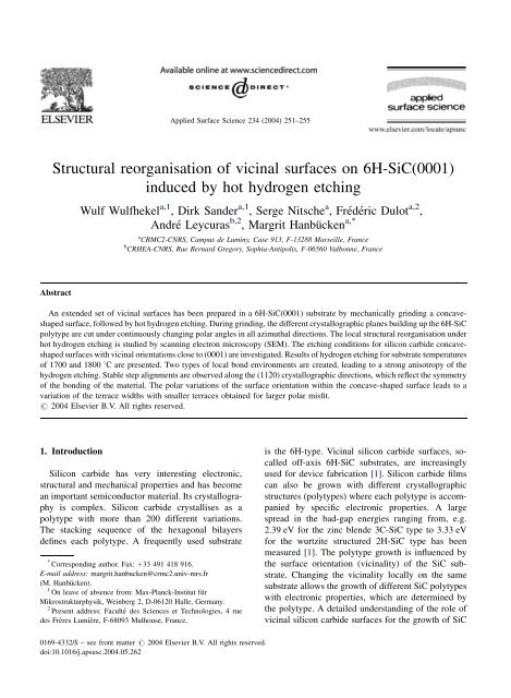
Structural reorganisation of vicinal surfaces on 6H-SiC(0001 ...
Structural reorganisation of vicinal surfaces on 6H-SiC(0001 ...
Structural reorganisation of vicinal surfaces on 6H-SiC(0001 ...

Create successful ePaper yourself
Turn your PDF publications into a flip-book with our unique Google optimized e-Paper software.
<str<strong>on</strong>g>Structural</str<strong>on</strong>g> <str<strong>on</strong>g>reorganisati<strong>on</strong></str<strong>on</strong>g> <str<strong>on</strong>g>of</str<strong>on</strong>g> <str<strong>on</strong>g>vicinal</str<strong>on</strong>g> <str<strong>on</strong>g>surfaces</str<strong>on</strong>g> <strong>on</strong> <strong>6H</strong>-<strong>SiC</strong>(<strong>0001</strong>)<br />
induced by hot hydrogen etching<br />
Abstract<br />
Wulf Wulfhekel a,1 , Dirk Sander a,1 , Serge Nitsche a , Frédéric Dulot a,2 ,<br />
André Leycuras b,2 , Margrit Hanbücken a,*<br />
a CRMC2-CNRS, Campus de Luminy, Case 913, F-13288 Marseille, France<br />
b CRHEA-CNRS, Rue Bernard Gregory, Sophia-Antipolis, F-06560 Valb<strong>on</strong>ne, France<br />
An extended set <str<strong>on</strong>g>of</str<strong>on</strong>g> <str<strong>on</strong>g>vicinal</str<strong>on</strong>g> <str<strong>on</strong>g>surfaces</str<strong>on</strong>g> has been prepared in a <strong>6H</strong>-<strong>SiC</strong>(<strong>0001</strong>) substrate by mechanically grinding a c<strong>on</strong>caveshaped<br />
surface, followed by hot hydrogen etching. During grinding, the different crystallographic planes building up the <strong>6H</strong>-<strong>SiC</strong><br />
polytype are cut under c<strong>on</strong>tinuously changing polar angles in all azimuthal directi<strong>on</strong>s. The local structural <str<strong>on</strong>g>reorganisati<strong>on</strong></str<strong>on</strong>g> under<br />
hot hydrogen etching is studied by scanning electr<strong>on</strong> microscopy (SEM). The etching c<strong>on</strong>diti<strong>on</strong>s for silic<strong>on</strong> carbide c<strong>on</strong>caveshaped<br />
<str<strong>on</strong>g>surfaces</str<strong>on</strong>g> with <str<strong>on</strong>g>vicinal</str<strong>on</strong>g> orientati<strong>on</strong>s close to (<strong>0001</strong>) are investigated. Results <str<strong>on</strong>g>of</str<strong>on</strong>g> hydrogen etching for substrate temperatures<br />
<str<strong>on</strong>g>of</str<strong>on</strong>g> 1700 and 1800 8C are presented. Two types <str<strong>on</strong>g>of</str<strong>on</strong>g> local b<strong>on</strong>d envir<strong>on</strong>ments are created, leading to a str<strong>on</strong>g anisotropy <str<strong>on</strong>g>of</str<strong>on</strong>g> the<br />
hydrogen etching. Stable step alignments are observed al<strong>on</strong>g the (1120) crystallographic directi<strong>on</strong>s, which reflect the symmetry<br />
<str<strong>on</strong>g>of</str<strong>on</strong>g> the b<strong>on</strong>ding <str<strong>on</strong>g>of</str<strong>on</strong>g> the material. The polar variati<strong>on</strong>s <str<strong>on</strong>g>of</str<strong>on</strong>g> the surface orientati<strong>on</strong> within the c<strong>on</strong>cave-shaped surface leads to a<br />
variati<strong>on</strong> <str<strong>on</strong>g>of</str<strong>on</strong>g> the terrace widths with smaller terraces obtained for larger polar misfit.<br />
# 2004 Elsevier B.V. All rights reserved.<br />
1. Introducti<strong>on</strong><br />
Applied Surface Science 234 (2004) 251–255<br />
Silic<strong>on</strong> carbide has very interesting electr<strong>on</strong>ic,<br />
structural and mechanical properties and has become<br />
an important semic<strong>on</strong>ductor material. Its crystallography<br />
is complex. Silic<strong>on</strong> carbide crystallises as a<br />
polytype with more than 200 different variati<strong>on</strong>s.<br />
The stacking sequence <str<strong>on</strong>g>of</str<strong>on</strong>g> the hexag<strong>on</strong>al bilayers<br />
defines each polytype. A frequently used substrate<br />
* Corresp<strong>on</strong>ding author. Fax: þ33 491 418 916.<br />
E-mail address: margrit.hanbucken@crmc2.univ-mrs.fr<br />
(M. Hanbücken).<br />
1 On leave <str<strong>on</strong>g>of</str<strong>on</strong>g> absence from: Max-Planck-Institut für<br />
Mikrostrukturphysik, Weinberg 2, D-06120 Halle, Germany.<br />
2 Present address: Faculté des Sciences et Technologies, 4 rue<br />
des Frères Lumière, F-68093 Mulhouse, France.<br />
0169-4332/$ – see fr<strong>on</strong>t matter # 2004 Elsevier B.V. All rights reserved.<br />
doi:10.1016/j.apsusc.2004.05.262<br />
is the <strong>6H</strong>-type. Vicinal silic<strong>on</strong> carbide <str<strong>on</strong>g>surfaces</str<strong>on</strong>g>, socalled<br />
<str<strong>on</strong>g>of</str<strong>on</strong>g>f-axis <strong>6H</strong>-<strong>SiC</strong> substrates, are increasingly<br />
used for device fabricati<strong>on</strong> [1]. Silic<strong>on</strong> carbide films<br />
can also be grown with different crystallographic<br />
structures (polytypes) where each polytype is accompanied<br />
by specific electr<strong>on</strong>ic properties. A large<br />
spread in the bad-gap energies ranging from, e.g.<br />
2.39 eV for the zinc blende 3C-<strong>SiC</strong> type to 3.33 eV<br />
for the wurtzite structured 2H-<strong>SiC</strong> type has been<br />
measured [1]. The polytype growth is influenced by<br />
the surface orientati<strong>on</strong> (<str<strong>on</strong>g>vicinal</str<strong>on</strong>g>ity) <str<strong>on</strong>g>of</str<strong>on</strong>g> the <strong>SiC</strong> substrate.<br />
Changing the <str<strong>on</strong>g>vicinal</str<strong>on</strong>g>ity locally <strong>on</strong> the same<br />
substrate allows the growth <str<strong>on</strong>g>of</str<strong>on</strong>g> different <strong>SiC</strong> polytypes<br />
with electr<strong>on</strong>ic properties, which are determined by<br />
the polytype. A detailed understanding <str<strong>on</strong>g>of</str<strong>on</strong>g> the role <str<strong>on</strong>g>of</str<strong>on</strong>g><br />
<str<strong>on</strong>g>vicinal</str<strong>on</strong>g> silic<strong>on</strong> carbide <str<strong>on</strong>g>surfaces</str<strong>on</strong>g> for the growth <str<strong>on</strong>g>of</str<strong>on</strong>g> <strong>SiC</strong>
252 W. Wulfhekel et al. / Applied Surface Science 234 (2004) 251–255<br />
films is <str<strong>on</strong>g>of</str<strong>on</strong>g> great importance for both, fundamental<br />
aspects <str<strong>on</strong>g>of</str<strong>on</strong>g> <strong>SiC</strong> growth and for technological applicati<strong>on</strong>s<br />
[2]. For example, the growth <str<strong>on</strong>g>of</str<strong>on</strong>g> nitrides like GaN<br />
<strong>on</strong> <str<strong>on</strong>g>vicinal</str<strong>on</strong>g> <strong>SiC</strong> <str<strong>on</strong>g>surfaces</str<strong>on</strong>g> can be performed without the<br />
formati<strong>on</strong> <str<strong>on</strong>g>of</str<strong>on</strong>g> detrimental screw-dislocati<strong>on</strong>s [3]. The<br />
c<strong>on</strong>trol <str<strong>on</strong>g>of</str<strong>on</strong>g> the substrate step density by adjusting the<br />
<str<strong>on</strong>g>vicinal</str<strong>on</strong>g> surface orientati<strong>on</strong> allows the growth <str<strong>on</strong>g>of</str<strong>on</strong>g> <strong>SiC</strong><br />
films with <strong>on</strong>e defined crystallographic structure (single<br />
polytype) via the so called ‘‘step c<strong>on</strong>trolled epitaxy’’<br />
[4].<br />
In previous experiments <strong>on</strong> silic<strong>on</strong>, a universal<br />
sample for the study <str<strong>on</strong>g>of</str<strong>on</strong>g> <str<strong>on</strong>g>vicinal</str<strong>on</strong>g> <str<strong>on</strong>g>surfaces</str<strong>on</strong>g> has been<br />
obtained, by transforming c<strong>on</strong>cave-shaped <str<strong>on</strong>g>surfaces</str<strong>on</strong>g><br />
into an extended set <str<strong>on</strong>g>of</str<strong>on</strong>g> <str<strong>on</strong>g>vicinal</str<strong>on</strong>g>s through thermal<br />
treatment [5,6]. In the case <str<strong>on</strong>g>of</str<strong>on</strong>g> Si(111) these curved<br />
<str<strong>on</strong>g>surfaces</str<strong>on</strong>g> split up into terraces. Surface morphology<br />
and step orientati<strong>on</strong> reflect the threefold symmetry <str<strong>on</strong>g>of</str<strong>on</strong>g><br />
the crystal. In extensi<strong>on</strong> <str<strong>on</strong>g>of</str<strong>on</strong>g> our previous work <strong>on</strong> Si,<br />
our objective is to investigate the influence <str<strong>on</strong>g>of</str<strong>on</strong>g> a locally<br />
varying surface orientati<strong>on</strong> <str<strong>on</strong>g>of</str<strong>on</strong>g> a <strong>SiC</strong> sample <strong>on</strong> the<br />
final morphology after hot hydrogen etching. In preliminary<br />
experiments [7] we have observed the morphological<br />
<str<strong>on</strong>g>reorganisati<strong>on</strong></str<strong>on</strong>g> <str<strong>on</strong>g>of</str<strong>on</strong>g> c<strong>on</strong>cave-shaped <str<strong>on</strong>g>surfaces</str<strong>on</strong>g><br />
due to hydrogen etching at 1700 8C. The resulting<br />
morphology was still rough, with a preferential step<br />
alignment in (1120) directi<strong>on</strong>s. Here, we present<br />
successful hydrogen etching experiments which lead<br />
to a regular and smooth structural <str<strong>on</strong>g>reorganisati<strong>on</strong></str<strong>on</strong>g>s <str<strong>on</strong>g>of</str<strong>on</strong>g><br />
the initially rough <str<strong>on</strong>g>surfaces</str<strong>on</strong>g>.<br />
2. Experimental<br />
The samples (4 mm 15 mm) were cut from an <strong>on</strong>axis,<br />
nitrogen doped, n-type (resistivity 0.03–<br />
0.12 O cm) <strong>6H</strong>-<strong>SiC</strong>(<strong>0001</strong>) wafer [8]. A c<strong>on</strong>caveshaped<br />
surface depressi<strong>on</strong> was created in the middle<br />
<str<strong>on</strong>g>of</str<strong>on</strong>g> the sample by a dimple grinder, using diam<strong>on</strong>d<br />
paste with a grain size <str<strong>on</strong>g>of</str<strong>on</strong>g> 3 mm. Grinding was stopped<br />
when a depth <str<strong>on</strong>g>of</str<strong>on</strong>g> about 30 mm was obtained in the<br />
middle <str<strong>on</strong>g>of</str<strong>on</strong>g> the dimple. The diameter <str<strong>on</strong>g>of</str<strong>on</strong>g> the dimple was<br />
about 1.5 mm, as checked by scanning electr<strong>on</strong> microscopy<br />
(SEM). For the given geometry, the in-plane<br />
azimuthal angle j varied for all samples from 0 < j <<br />
3608 and the out-<str<strong>on</strong>g>of</str<strong>on</strong>g>-plane polar angle y varied for the<br />
analysed samples from 08 in the middle <str<strong>on</strong>g>of</str<strong>on</strong>g> the dimple<br />
to about maximum 2–48 as determined through geometrical<br />
c<strong>on</strong>siderati<strong>on</strong>s. Prior to hydrogen (H2) etch-<br />
ing, the samples were cleaned in an ultras<strong>on</strong>ic bath <str<strong>on</strong>g>of</str<strong>on</strong>g><br />
trichlorethylene, then acet<strong>on</strong>e, and finally methanol.<br />
H2 etching was performed in a horiz<strong>on</strong>tal graphite hotwall<br />
chemical vapour depositi<strong>on</strong> (CVD) reactor [9] at<br />
an H 2 pressure <str<strong>on</strong>g>of</str<strong>on</strong>g> 13 mbar. The etching temperature<br />
was varied between 1700 and 1800 8C, and the etching<br />
time, i.e. the time <str<strong>on</strong>g>of</str<strong>on</strong>g> exposure <str<strong>on</strong>g>of</str<strong>on</strong>g> the sample at high<br />
temperature to H2 was varied between 20 min and 1 h.<br />
The resulting structural reorganizati<strong>on</strong> is compared to<br />
our previous experiments, which were performed at an<br />
etching temperature <str<strong>on</strong>g>of</str<strong>on</strong>g> 1700 8C and equal etching<br />
times [7]. The etched samples were subsequently<br />
characterised by SEM. The effect <str<strong>on</strong>g>of</str<strong>on</strong>g> hydrogen etching<br />
<strong>on</strong> the various <strong>SiC</strong> surface orientati<strong>on</strong>s as prepared by<br />
dimple grinding was investigated. For comparis<strong>on</strong>,<br />
SEM images were also taken <strong>on</strong> the flat parts <str<strong>on</strong>g>of</str<strong>on</strong>g> the<br />
<strong>SiC</strong> substrate outside the dimple area.<br />
3. Results and discussi<strong>on</strong><br />
A c<strong>on</strong>cave-shaped surface was obtained <strong>on</strong> a flat<br />
<strong>6H</strong>-<strong>SiC</strong>(<strong>0001</strong>) sample by dimple grinding. Fig. 1<br />
shows a schematic view <str<strong>on</strong>g>of</str<strong>on</strong>g> a typical sample. Images<br />
were taken <strong>on</strong> different areas <strong>on</strong> the c<strong>on</strong>cave-shaped<br />
surface within the dimple area and, for comparis<strong>on</strong>,<br />
also <strong>on</strong> the adjacent flat parts outside the dimple area.<br />
The hydrogen etching c<strong>on</strong>diti<strong>on</strong>s required to remove<br />
the initial roughness <strong>on</strong> flat <strong>SiC</strong> <str<strong>on</strong>g>surfaces</str<strong>on</strong>g> are well<br />
known in the literature [10,11]. When etched for<br />
30 min at 1550 8C under a hydrogen flux at atmospheric<br />
pressure [10] all scratches are removed from<br />
the flat parts <str<strong>on</strong>g>of</str<strong>on</strong>g> the substrate. A well-defined distributi<strong>on</strong><br />
<str<strong>on</strong>g>of</str<strong>on</strong>g> flat terraces and steps is created. These steps are<br />
very straight and their heights is 0.75 or 1.5 nm<br />
corresp<strong>on</strong>ding to half or a complete lattice distance<br />
in the c-axis (three or six <strong>SiC</strong> bilayers).<br />
Fig. 1. Sketch <str<strong>on</strong>g>of</str<strong>on</strong>g> the c<strong>on</strong>cave-shaped surface (called ‘‘dimple’’)<br />
produced in a <strong>6H</strong>-<strong>SiC</strong>(0 0 0 1) surface using a dimple grinder (see<br />
text for details).
However, the etch rate within the dimple area was<br />
found to depend <strong>on</strong> the sample disorientati<strong>on</strong>. On <str<strong>on</strong>g>of</str<strong>on</strong>g>faxis<br />
substrates the etch rate was found to be 30–40%<br />
smaller than <strong>on</strong> <strong>on</strong>-axis substrates [12]. In the present<br />
work, a systematic study <str<strong>on</strong>g>of</str<strong>on</strong>g> the morphological variati<strong>on</strong>s<br />
induced through different polar and azimuthal<br />
disorientati<strong>on</strong>s, was d<strong>on</strong>e by analyzing SEM images,<br />
which were taken at selected areas within the dimple.<br />
Before we start the discussi<strong>on</strong> <str<strong>on</strong>g>of</str<strong>on</strong>g> our results, we<br />
present in Fig. 2 a sketch <str<strong>on</strong>g>of</str<strong>on</strong>g> the crystallography <str<strong>on</strong>g>of</str<strong>on</strong>g> the<br />
<strong>6H</strong>-<strong>SiC</strong>(0 001)polytype <str<strong>on</strong>g>of</str<strong>on</strong>g> our substrate. Al<strong>on</strong>g the<br />
c-axis <str<strong>on</strong>g>of</str<strong>on</strong>g> the crystal, i.e. the vertical directi<strong>on</strong> <str<strong>on</strong>g>of</str<strong>on</strong>g> Fig. 2,<br />
six hexag<strong>on</strong>al <strong>SiC</strong> bilayers are arranged in two groups<br />
<str<strong>on</strong>g>of</str<strong>on</strong>g> three bilayers each. Within each group, the stacking<br />
is hexag<strong>on</strong>al, but from <strong>on</strong>e group to the other, the<br />
lattice is rotated by 608. As a c<strong>on</strong>sequence, the closepacked<br />
step edges <strong>on</strong> <strong>6H</strong>-<strong>SiC</strong> change their nature<br />
going from <strong>on</strong>e group to the other. The character <str<strong>on</strong>g>of</str<strong>on</strong>g><br />
steps running al<strong>on</strong>g low index directi<strong>on</strong>s alternates<br />
and shows either <strong>on</strong>e (SN) or two (SD) dangling b<strong>on</strong>ds<br />
(step nomenclature according to Pechman et al. [13]).<br />
Fig. 2(b) shows a cross-secti<strong>on</strong>al view al<strong>on</strong>g the<br />
{2110} directi<strong>on</strong>. The two groups <str<strong>on</strong>g>of</str<strong>on</strong>g> step edges are<br />
indicated by the number <str<strong>on</strong>g>of</str<strong>on</strong>g> dangling b<strong>on</strong>ds. The same<br />
W. Wulfhekel et al. / Applied Surface Science 234 (2004) 251–255 253<br />
Fig. 2. (a) Crystallographic stacking <str<strong>on</strong>g>of</str<strong>on</strong>g> the <strong>SiC</strong> bilayers in a <strong>6H</strong>-<strong>SiC</strong>(0 0 0 1) crystal. (b) Atomic b<strong>on</strong>ds <strong>on</strong> step risers in the {0 1 1 0} directi<strong>on</strong><br />
viewed from the {2 1 1 0} directi<strong>on</strong>. The b<strong>on</strong>d c<strong>on</strong>figurati<strong>on</strong> corresp<strong>on</strong>ds to steps with three bilayer-height steps. Larger circles stand for Si and<br />
smaller circles for C atoms.<br />
sequence <str<strong>on</strong>g>of</str<strong>on</strong>g> two dangling b<strong>on</strong>ds for a cut al<strong>on</strong>g the<br />
vertical directi<strong>on</strong> in the lower three bilayers versus <strong>on</strong>e<br />
dangling b<strong>on</strong>d in the upper three bilayers can also be<br />
extracted from Fig. 2(a). The building block <str<strong>on</strong>g>of</str<strong>on</strong>g> the<br />
structure, a fourfold co-ordinated Si atom, is rotated<br />
by 608 when going from the lower to the upper half.<br />
Therefore, the co-ordinati<strong>on</strong> <str<strong>on</strong>g>of</str<strong>on</strong>g> a Si atom with a C<br />
neighbour <strong>on</strong> the right-hand side changes from tw<str<strong>on</strong>g>of</str<strong>on</strong>g>old<br />
to <strong>on</strong>efold.<br />
Our results indicate that the hydrogen etching<br />
behaviour is str<strong>on</strong>gly influenced by these variati<strong>on</strong>s<br />
<str<strong>on</strong>g>of</str<strong>on</strong>g> the local b<strong>on</strong>ding structure. As a c<strong>on</strong>sequence, <strong>SiC</strong><br />
erosi<strong>on</strong> <strong>on</strong> <str<strong>on</strong>g>vicinal</str<strong>on</strong>g> <str<strong>on</strong>g>surfaces</str<strong>on</strong>g> is highly anisotropic. Fig. 3<br />
shows SEM images obtained <strong>on</strong> equivalent part <strong>on</strong> the<br />
c<strong>on</strong>cave-shaped surface. The etching c<strong>on</strong>diti<strong>on</strong>s were<br />
changed from (a) to (b). The sample in (a) was etched<br />
for 60 min at 1700 8C whereas the sample in (b) was<br />
etched additi<strong>on</strong>ally at 1800 8C for 20 min. The etching<br />
c<strong>on</strong>diti<strong>on</strong>s used in (a) result in the appearance <str<strong>on</strong>g>of</str<strong>on</strong>g> a<br />
predominance <str<strong>on</strong>g>of</str<strong>on</strong>g> the most stable step edges, which run<br />
al<strong>on</strong>g the family <str<strong>on</strong>g>of</str<strong>on</strong>g> {1120} directi<strong>on</strong>s, <strong>on</strong>e <str<strong>on</strong>g>of</str<strong>on</strong>g> the<br />
closed-packed step directi<strong>on</strong>s. This allows the energetically<br />
stable formati<strong>on</strong> <str<strong>on</strong>g>of</str<strong>on</strong>g> l<strong>on</strong>g and straight step<br />
edges. Hydrogen etching at a substrate temperature <str<strong>on</strong>g>of</str<strong>on</strong>g>
254 W. Wulfhekel et al. / Applied Surface Science 234 (2004) 251–255<br />
Fig. 3. SEM images <str<strong>on</strong>g>of</str<strong>on</strong>g> an (a) area <strong>on</strong> the c<strong>on</strong>cave-shaped surface after H2 erosi<strong>on</strong> for 1 h at 1700 8C; (b) equivalent area <strong>on</strong> the same sample<br />
after an additi<strong>on</strong>al H 2 erosi<strong>on</strong> at 1800 8C for 20 min.<br />
Fig. 4. (a,c,d) SEM images taken <strong>on</strong> different areas <str<strong>on</strong>g>of</str<strong>on</strong>g> the reorganised c<strong>on</strong>cave-shaped surface, the inset in (a) shows a zoom <str<strong>on</strong>g>of</str<strong>on</strong>g> the same area.<br />
(b) indicates the locati<strong>on</strong> <str<strong>on</strong>g>of</str<strong>on</strong>g> the imaged areas within the dimple.
18008 enables the removal <str<strong>on</strong>g>of</str<strong>on</strong>g> all rough step bunches,<br />
which are still visible in (a), but which are absent in<br />
(b). Very straight and regular steps were obtained,<br />
which give rise to a very narrow terrace width distributi<strong>on</strong><br />
with a parallel step orientati<strong>on</strong> al<strong>on</strong>g<br />
{1 1 2 0}. SEM studies have been performed <strong>on</strong><br />
selected parts <str<strong>on</strong>g>of</str<strong>on</strong>g> the dimple to study the influence<br />
<str<strong>on</strong>g>of</str<strong>on</strong>g> the azimuthal directi<strong>on</strong> <strong>on</strong> the structural re-organisati<strong>on</strong><br />
within the c<strong>on</strong>cave-shaped surface.. The chosen<br />
areas reflect the symmetry <str<strong>on</strong>g>of</str<strong>on</strong>g> the crystal. Fig. 4(a),<br />
(c) and (d) show SEM images <str<strong>on</strong>g>of</str<strong>on</strong>g> areas as indicated in<br />
Fig. 4(b). As already shown in Fig. 3, <strong>on</strong> all areas a<br />
very smooth morphology with very regular, straight<br />
step edges was observed. The step directi<strong>on</strong> shows<br />
systematic changes depending <strong>on</strong> the azimuthal misorientati<strong>on</strong><br />
in the dimple. Three different energetically<br />
stable alignments can be distinguished. In (a) this<br />
directi<strong>on</strong> corresp<strong>on</strong>ds to the family <str<strong>on</strong>g>of</str<strong>on</strong>g> {1 1 2 0} directi<strong>on</strong>s,<br />
in (c) and (d) they follow the {2 1 1 0} and<br />
{121 0} directi<strong>on</strong>s, respectively. Line scans al<strong>on</strong>g<br />
the SEM images <str<strong>on</strong>g>of</str<strong>on</strong>g> the curved surface area at a fixed<br />
azimuthal angle give a first, rough analysis <str<strong>on</strong>g>of</str<strong>on</strong>g> the<br />
morphological changes as a functi<strong>on</strong> <str<strong>on</strong>g>of</str<strong>on</strong>g> the polar misorientati<strong>on</strong>.<br />
The SEM images shown in Fig. 4 reflect<br />
some dependences for small polar angles. In (c) the<br />
terrace width is around 1 mm whereas in (d) steps are<br />
separated by terraces around 300 nm wide. This larger<br />
terrace size in (c) as compared to (b) reflects the smaller<br />
polar misfit <str<strong>on</strong>g>of</str<strong>on</strong>g> area (c) due its closer proximity to the<br />
centre <str<strong>on</strong>g>of</str<strong>on</strong>g> the dimple. More detailed experiments with<br />
increased lateral resoluti<strong>on</strong> were performed by AFM<br />
and will be published elsewhere [14].<br />
4. Summary and outlook<br />
Etching c<strong>on</strong>diti<strong>on</strong>s (substrate temperature: 1800 8C,<br />
etching time: 20 min, hydrogen flux: 13 mbar) leading<br />
to very smooth structural <str<strong>on</strong>g>reorganisati<strong>on</strong></str<strong>on</strong>g>s <str<strong>on</strong>g>of</str<strong>on</strong>g> initially<br />
rough, curved silic<strong>on</strong> carbide <str<strong>on</strong>g>surfaces</str<strong>on</strong>g> were established.<br />
First results obtained by SEM show straight step alignments<br />
in some distinct, energetically stable directi<strong>on</strong>s.<br />
Step heights <str<strong>on</strong>g>of</str<strong>on</strong>g> 1.5 nm corresp<strong>on</strong>ding to the height <str<strong>on</strong>g>of</str<strong>on</strong>g><br />
<strong>on</strong>e unit cell <str<strong>on</strong>g>of</str<strong>on</strong>g> <strong>6H</strong>-<strong>SiC</strong> were imaged. A more detailed<br />
study by scanning tunnelling- and atomic force micro-<br />
W. Wulfhekel et al. / Applied Surface Science 234 (2004) 251–255 255<br />
scopy <str<strong>on</strong>g>of</str<strong>on</strong>g> the polar and azimuthal dependencies <str<strong>on</strong>g>of</str<strong>on</strong>g> the<br />
observed step arrangements are in preparati<strong>on</strong> and will<br />
be published elsewhere [14].<br />
Acknowledgements<br />
DS and WW gratefully acknowledge the friendly<br />
hospitality and support by the CNRS, the Université<br />
d’Aix-Marseille 2 and the CRMC2. MH gratefully<br />
acknowledges the friendly hospitality <str<strong>on</strong>g>of</str<strong>on</strong>g> the Max-<br />
Planck-Institut für Mikrostrukturphysik. FD gratefully<br />
acknowledges the c<strong>on</strong>tinuous hospitality <str<strong>on</strong>g>of</str<strong>on</strong>g> the<br />
CRMC2. Very efficient help <str<strong>on</strong>g>of</str<strong>on</strong>g> Francis Quintric,<br />
CRMC2, is acknowledged.<br />
References<br />
[1] W.J. Choyke, Optical and electric properties <str<strong>on</strong>g>of</str<strong>on</strong>g> <strong>SiC</strong>, in: R.<br />
Freer (Ed.), The Physics and Chemistry <str<strong>on</strong>g>of</str<strong>on</strong>g> Carbides, Nitrides<br />
and Borides, NATO ASI Series, Manchester, 1989.<br />
[2] K. Heinz, U. Starke, J. Bernhardt, J. Schardt, Appl. Surf. Sci.<br />
162–163 (2000) 9.<br />
[3] M.H. Xie, L.X. Zheng, S.H. Cheung, Y.F. Ng, H. Wu, S.Y.<br />
T<strong>on</strong>gand, N. Ohtani, Appl. Phys. Lett. 77 (2000) 1105.<br />
[4] T. Ueda, H. Nishino, H. Matsunami, J. Cryst. Growth 104<br />
(1990) 695.<br />
[5] M. Hanbücken, B. Röttger, R. Kliese, I. Vianey, H.<br />
Neddermeyer, Europhys. Lett. 23 (1993) 573.<br />
[6] M. Hanbücken, B. Röttger, H. Neddermeyer, Surf. Sci. 331–<br />
333 (1995) 1028.<br />
[7] F. Dulot, L. Mansour, A. Leycuras, W. Wulfhekel, D. Sander,<br />
F. Arnaud d’Avitaya, M. Hanbücken, Appl. Surf. Sci. 187<br />
(2002) 319.<br />
[8] <strong>SiC</strong>rystal AG, Erlangen, Germany. http://www.sicrystal.de.<br />
[9] A. Leycuras, Mater. Sci. Forum 338–342 (2000) 241.<br />
[10] F. Owman, C. Hallin, P. Ma˚rtenss<strong>on</strong>, E. Janzén, J. Cryst.<br />
Growth 167 (1996) 391.<br />
[11] N. Ohtani, M. Katsuno, T. Aigo, T. Fujimoto, H. Tsuge, H.<br />
Yashiro, M. Kanaya, J. Cryst. Growth 210 (2000) 613;<br />
C. Hallin, F. Owman, P. Martenss<strong>on</strong>, A. Ellis<strong>on</strong>, A.<br />
K<strong>on</strong>stantinov, O. Kordina, E. Janzen, J. Cryst. Growth 181<br />
(1997) 241.<br />
[12] Z.Y. Xie, C.H. Wei, L.Y. Li, Q.M. Yu, J.H. Edgar, J. Cryst.<br />
Growth 217 (2000) 115.<br />
[13] R.J. Pechman, X.-S. Wang, J.H. Weaver, Phys. Rev. B 52<br />
(1995) 11412.<br />
[14] H. Diesinger, E. Moyer, W. Wulfhekel, D. Sander, S. Nitsche,<br />
A. Leycuras, M. Hanbücken, in preparati<strong>on</strong>.