
You also want an ePaper? Increase the reach of your titles
YUMPU automatically turns print PDFs into web optimized ePapers that Google loves.
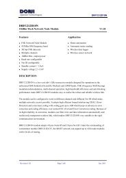
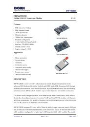
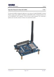
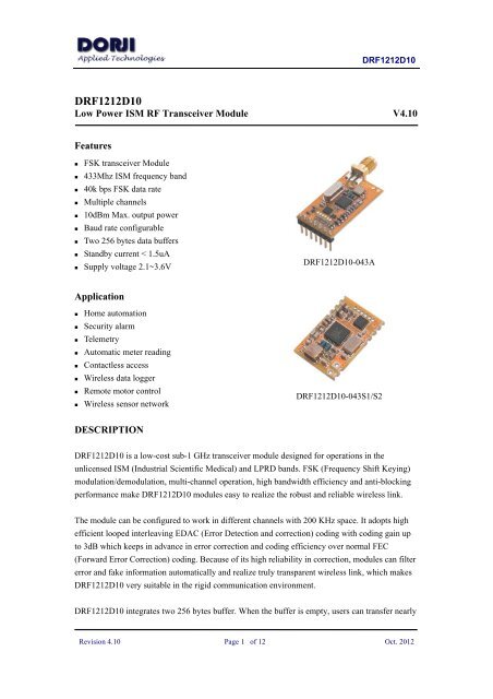
<strong>DRF1212D10</strong><br />
<strong>DRF1212D10</strong><br />
Low Power ISM RF Transceiver Module V4.10<br />
Features<br />
� FSK transceiver Module<br />
� 433Mhz ISM frequency band<br />
� 40k bps FSK data rate<br />
� Multiple channels<br />
� 10dBm Max. output power<br />
� Baud rate configurable<br />
� Two 256 bytes data buffers<br />
� Standby current < 1.5uA<br />
� Supply voltage 2.1~3.6V<br />
Application<br />
� Home automation<br />
� Security alarm<br />
� Telemetry<br />
� Automatic meter reading<br />
� Contactless access<br />
� Wireless data logger<br />
� Remote motor control<br />
� Wireless sensor network<br />
DESCRIPTION<br />
<strong>DRF1212D10</strong>-043A<br />
<strong>DRF1212D10</strong>-043S1/S2<br />
<strong>DRF1212D10</strong> is a low-cost sub-1 GHz transceiver module designed for operations in the<br />
unlicensed ISM (Industrial Scientific Medical) and LPRD bands. FSK (Frequency Shift Keying)<br />
modulation/demodulation, multi-channel operation, high bandwidth efficiency and anti-blocking<br />
performance make <strong>DRF1212D10</strong> modules easy to realize the robust and reliable wireless link.<br />
The module can be configured to work in different channels with 200 KHz space. It adopts high<br />
efficient looped interleaving EDAC (Error Detection and correction) coding with coding gain up<br />
to 3dB which keeps in advance in error correction and coding efficiency over normal FEC<br />
(Forward Error Correction) coding. Because of its high reliability in correction, modules can filter<br />
error and fake information automatically and realize truly transparent wireless link, which makes<br />
<strong>DRF1212D10</strong> very suitable in the rigid communication environment.<br />
<strong>DRF1212D10</strong> integrates two 256 bytes buffer. When the buffer is empty, users can transfer nearly<br />
Revision 4.10 Page 1 of 12 Oct. 2012
<strong>DRF1212D10</strong><br />
217 bytes data per time and even limitless data transfer can be achieved as long as RF data rate<br />
(RF module to RF module) is configured to be faster than UART data rate (MCU to RF module).<br />
<strong>DRF1212D10</strong> provides standard UART/TTL interface. Users can choose seven data rates and<br />
three parity checks which make <strong>DRF1212D10</strong> possibly tailor-made for different applications.<br />
<strong>DRF1212D10</strong> operates at 2.1~3.6V with extra low power consumption. The current in sleep mode<br />
can be minimized to 1.5uA and the current in receive mode no more than 3mA makes modules<br />
very suitable for battery powered-up applications.<br />
PIN FUNCTIONS<br />
PIN DIP-A Function SMD-S1/S2 Description<br />
1 GND Ground GND Ground (0V)<br />
2 VCC Power VCC Power supply<br />
3 SETA Input SETB SETA: Parameter setting A; pull-up resistor: 47K Ohm<br />
4 RXD Input AUX RXD: UART input, TTL level; pull-up resistor:47K Ohm<br />
5 TXD Output SETA TXD: UART output, TTL level<br />
6 AUX Output TXD AUX: Data In/out indication<br />
7 SETB Input RXD SETB: Parameter setting B; pull-up resistor: 1M Ohm<br />
8 --- GND Ground (0V)<br />
9 --- GND Ground (0V)<br />
10 --- ANT Antenna Port<br />
ELECTRICAL SPECIFICATIONS<br />
Table 1 <strong>DRF1212D10</strong> Pin functions<br />
Symbol Parameter (condition) Min. Typ. Max. Units<br />
VCC Supply Voltage 2.1 3.6 V<br />
Temp Operating temperature range -20 25 70 °C<br />
RH Operating relative humidity 10 90 %<br />
Freq Frequency range 430 437 MHz<br />
FDEV Modulation deviation 67 KHz<br />
Mod Modulation type FSK<br />
IDD Receive mode @1K bps<br />
2.7<br />
mA<br />
Receive mode @10K bps<br />
3.0<br />
mA<br />
Receive mode @40K bps<br />
4.0<br />
mA<br />
Transmit mode @ 0dBm<br />
20<br />
mA<br />
Transmit mode @ 10dBm<br />
35<br />
mA<br />
Sleep mode<br />
1.5 2.5 uA<br />
Pout Maximum output power 10 dBm<br />
Revision 4.10 Page 2 of 12 Oct. 2012
<strong>DRF1212D10</strong><br />
Sen Receiving sensitivity @1K bps<br />
-113<br />
dBm<br />
Receiving sensitivity @10K bps<br />
-107<br />
dBm<br />
DRFSK FSK data rate 1 40 Kbps<br />
DRIN UART data rate 1.2 57.6 Kbps<br />
TR (1) Wake-up & Search preamble time .@1K bps<br />
@2K bps<br />
@5K bps<br />
@10K bps<br />
@20K bps<br />
@40K bps<br />
TS (2) Switching time 20 us<br />
CHBW Channel spacing 200 KHz<br />
ZANT Antenna Impedance 50 Ohm<br />
Revision 4.10 Page 3 of 12 Oct. 2012<br />
20<br />
12<br />
6.2<br />
4.2<br />
3.3<br />
2.8<br />
Table 2 <strong>DRF1212D10</strong> Electrical Specifications<br />
Note:<br />
(1). If the receiver is configured to work in PWR-saving mode, it will wake up at fixed interval which can<br />
be set through MCU or configuration board. The parameter TR is the total time which includes the time<br />
that receiver resumes normal receive status from sleep mode (crystal, I/O port and other circuits are<br />
triggered) and the time (about 16-bit long) that receiver searches the preamble.<br />
(2). When <strong>DRF1212D10</strong> is in sleep mode, users can set the pin SETA of module to low to activate it. The<br />
parameter TS refers the time which the module wakes up from sleep mode and monitors the serial port<br />
if there is any data from MCU.<br />
ABSOLUTE MAXIMUM RATINGS<br />
Symbol Parameter Min. Max. Units<br />
VCC Supply Voltage -0.3 3.7 V<br />
VI Input voltage -0.3 VCC+0.3 V<br />
VO Output voltage -0.3 VCC+0.3 V<br />
TST Storage temperature -55 125 °C<br />
APPLICATION INFORMATION<br />
1. CODING FORMAT<br />
Table 3 <strong>DRF1212D10</strong> Maximum Ratings<br />
PREAMBLE SYNCWORD ID (only for S2) DATA+FEC+CRC<br />
Table 4 <strong>DRF1212D10</strong> Coding Format<br />
ms<br />
ms<br />
ms<br />
ms<br />
ms<br />
ms
<strong>DRF1212D10</strong><br />
The preamble is alternative “1010” codes which is used to make the clock of receiver<br />
synchronous with transmitter. In normal conditions, 32-bit preamble is enough for use. When<br />
<strong>DRF1212D10</strong> works in power-saving mode, the preamble also can be functioned to wake up<br />
the receiver and it must be long enough in order to obtain such a function.<br />
E.g. if the receiver is configured to wake up at the interval of one second, it wakes up every<br />
other second and searches the preamble for 16-bit long time. In this case the transmitter must<br />
be configured to work in mode 2 so longer preamble code plus synchronous word will be sent,<br />
which means the receiver can detect the preamble in wake-up period successfully.<br />
2. WORKING MODE<br />
<strong>DRF1212D10</strong> can work in 4 different modes which can be configured through SETA and<br />
SETB pins.<br />
Mode SETA SETB Description Working Status<br />
1 0 0 Normal<br />
2 0 1 Wake-up<br />
3 1 0 PWR-saving<br />
Serial port enabled. Module works in continuous receive<br />
conditions. When data comes from MCU, AUX pin is set to<br />
low and module is switched to transmit status; then 32bits<br />
preamble and synchronous word will be sent. After data is<br />
transferred, AUX pin will be sent to high and the module will<br />
enter into continuous receiver status again.<br />
In this mode the preamble in transmitted data package is not<br />
long so the receiver module must work in Mode 1 or 2. When<br />
receiver module detects data in the present wireless channel,<br />
it will verify the data and set AUX pin to low and then output<br />
data to serial port after data is confirmed correctly.<br />
Serial port enabled. Module works in continuous receive<br />
conditions. When data comes from MCU, AUX pin is set to<br />
low and module is switched to transmit status; then preamble<br />
[ 1 wake-up period (E.g. 1s)+ 32bits] and synchronous will be<br />
sent. After data is transferred, AUX pin will be sent to high<br />
and the module will enter into continuous receiver status<br />
again. Because the longer preamble is introduced, the<br />
receiver module can work in Mode1, 2 or 3.<br />
When receiver module detects data in the present wireless<br />
channel, it will verify the data and set AUX pin to low and<br />
then output data to serial port after data is confirmed<br />
correctly.<br />
Serial port disabled. The receiver module wakes up at a preset<br />
period and search if there is any data coming in present<br />
channel. It will enter into sleep status when no signal is<br />
Revision 4.10 Page 4 of 12 Oct. 2012
<strong>DRF1212D10</strong><br />
detected. As soon as the preamble is sniffed out, the receiver<br />
module will keep in receive status and wait for the<br />
synchronous word; then it will verify the data and set AUX<br />
pin to low. After 5ms delay, the receiver module outputs data<br />
to serial port.<br />
After data is transferred, the serial port is disabled and AUX<br />
pin is set to high. The module will enter into sleep status<br />
again and wait for the next wake-up when mode setting isn’t<br />
changed<br />
4 1 1 Sleep<br />
Serial port disabled. The module stays in sleep status. In this<br />
mode. The RF circuit, the main clock circuit and peripherals<br />
are closed. The power consumption is extra low (about<br />
1.5uA).<br />
Table 5 <strong>DRF1212D10</strong> Working Mode<br />
Figure1: Transmit Module in Mode 2 and Receive Module in Mode 3<br />
<strong>DRF1212D10</strong> module enters into sleep mode by software control. In sleep mode the levels of<br />
serial port are kept in corresponding status and can be switched to any other status. It only needs<br />
20us to wake up the module from sleep mode, which means data can be output to serial port after<br />
SETA pin is set to low more than 20uS. When the module is in transmit or receive process, it only<br />
can enter PWR-saving or sleep mode after the transmitting or receiving process is finished even<br />
though the SETA pin is set to high. Users can take this advantage to set SETA pin to high and<br />
make the module enter into sleep status without waiting the finish of present transmit because the<br />
module will detect SETA pin after a data package is transferred.<br />
Revision 4.10 Page 5 of 12 Oct. 2012
3. PARAMETER SETTING<br />
<strong>DRF1212D10</strong><br />
Users can configure the parameters (frequency, data rate, output power, etc.) of RF modules<br />
by MCU or PC through converter boards DAC01 or DAC02.<br />
� BY PC This mode is only available for DIP package. The interface of <strong>DRF1212D10</strong> is<br />
UART/TTL. If connecting it to PC, users need to use a level converter board to transform<br />
the different levels. <strong>Dorji</strong> Applied Technologies provides converter boards DAC01<br />
(TTL-to-RS232) and DAC02 (TTL-to-USB) for configuration.<br />
Firstly users need to insert module into converter board and connect converter board to<br />
PC by cable, then open DORJI RF software. After that the status column of tool should<br />
display “Found Device”. Users then can read/write the module. For more details, please<br />
check the operation manuals of converter boards on accessory page.<br />
Figure 2: DRF TOOL for <strong>DRF1212D10</strong>-043A Module<br />
� BY MCU. The module can work normally after powering on for 50ms (T1) or more.<br />
When configuring the module, users need to switch it to Mode 4 and monitor AUX pin<br />
which should be in high level without any transmit or receive. The module then can be<br />
configured after it enters into sleep mode for 10uS or more (T2).<br />
When commands are output to RXD pin, the module will be waken up no matter what<br />
status of UART interface is in and it will use 9600 bps (data rate) and no parity check as<br />
default format to configure parameters. If the commands are set correctly, the module will<br />
feed back the written commands; then it will be reset and initialized. After 100ms (T4),<br />
Revision 4.10 Page 6 of 12 Oct. 2012
<strong>DRF1212D10</strong><br />
the module will work with the new parameters. Please note that if the commands are set<br />
incorrectly, the module will give no feedback but it will still be reset and initialized. Users<br />
can take this advantage to wake up modules in long-term sleep or reset the modules.<br />
Figure 3: Connecting Diagram Between <strong>DRF1212D10</strong> and MCU<br />
Figure 4: Timing Sequence for Setting Parameters<br />
The commands of <strong>DRF1212D10</strong> are in HEX format. The configuring data rate is 9600<br />
bps and no parity check included. The command set include two commands: Read<br />
command and Write command.<br />
Revision 4.10 Page 7 of 12 Oct. 2012
<strong>DRF1212D10</strong><br />
SMD package <strong>DRF1212D10</strong>-043S1 and <strong>DRF1212D10</strong>-043S2 type are the same in<br />
dimensions. The only difference in function is that <strong>DRF1212D10</strong>-043S2 has group ID<br />
which means only modules with the same ID can communicate. <strong>DRF1212D10</strong>-043S1<br />
doesn’t contain ID so it’s fully compatible with DIP package <strong>DRF1212D10</strong>-043D.<br />
1. DIP & S1 package<br />
Read command: 0xFF,0x56,0xAE,0x35,0xA9,0x55,0xF0<br />
Response: 0x24, 0x24, 0x24+Freq+DRFSK+POUT+DRIN+Parity+TW<br />
Write command: 0xFF,0x56,0xAE,0x35,0xA9,0x55,0x90+Freq+DRIN+POUT+DRFSK+<br />
Parity+TW<br />
Response: 0x24, 0x24, 0x24+Freq+DRFSK +POUT+ DRIN+Parity+TW<br />
2. S2 package<br />
Read command: 0xFF,0x56,0xAE,0x35,0xA9,0x55,0xF0<br />
Response: 0x24, 0x24, 0x24+Freq+DRFSK+POUT+DRIN+Parity+TW+ID<br />
Write command: 0xFF,0x56,0xAE,0x35,0xA9,0x55,0x90+Freq+DRIN+POUT+DRFSK+<br />
Parity+TW+ID<br />
Response: 0x24, 0x24, 0x24+Freq+DRFSK +POUT+ DRIN+Parity+TW+ID<br />
Parameter Unit Length Explanation<br />
Freq. KHz 3 433.92MHz = 0x06, 0x9F, 0x00<br />
DRFSK K bps 1 1, 2, 5,10, 20, 40 equals to 0x00,0x01,0x02,0x03,0x04,0x05<br />
POUT dB 1 From 0 to 7 represents 0x00 to 0x07. One increment<br />
increases 3dBm. “0x07” equals to the Max. output power<br />
(10dBm).<br />
DRIN Kbps 1 1.2, 2.4, 4.8, 9.6, 19.2, 38.4, 57.6 equals to<br />
Parity 1<br />
0x00,0x01,0x02,0x03,0x04,0x05,0x06<br />
0x00: No parity; 0x01: Even parity; 0x02: Odd parity<br />
TW S 1 0.05, 0.1, 0.2, 0.4, 0.6, 1, 1.5, 2, 2.5, 3, 4, 5 corresponding to<br />
0x00~0x0b<br />
ID 3 000001~FFFFFF, only available for S2 type<br />
Table 6: <strong>DRF1212D10</strong> Parameter Coding<br />
E.g. If the user wants to set the module work at Freq (433.92MHz), DRFSK (10K bps), POUT (10<br />
dBm), DRIN (9.6k bps), Parity (no parity), TW (1second wake-up period), the command for DIP<br />
or S1 type could be written as below:<br />
Revision 4.10 Page 8 of 12 Oct. 2012
<strong>DRF1212D10</strong><br />
Write Command: 0xFF,0x56,0xAE,0x35,0xA9,0x55,0x90, 0x06,0x9F,0x00, 0x03, 0x07,<br />
0x03, 0x00,0x05<br />
Response: 0x24,0x24,0x24, 0x06,0x9F,0x00, 0x03,0x07,0x03,0x00,0x05<br />
For S2 type with ID 0x000001<br />
Write Command: 0xFF,0x56,0xAE,0x35,0xA9,0x55,0x90, 0x06,0x9F,0x00, 0x03, 0x07,<br />
0x03, 0x00,0x05, 0x00, 0x00, 0x01<br />
Response: 0x24,0x24,0x24, 0x06,0x9F,0x00, 0x03,0x07,0x03,0x00,0x05, 0x00,<br />
0x00, 0x01<br />
<strong>DRF1212D10</strong> module can monitor the field strength (RSSI) dynamically. If <strong>DRF1212D10</strong> is in<br />
receive mode (SETA is low) and a positive pulse with width more than 200us is imposed on SETB,<br />
the module will output one byte field value at the falling edge of the pulse. The picture below<br />
shows the timing sequence.<br />
Figure 5: RSSI Timing Sequence<br />
Even though the positive pulse is imposed on SETB, it does not guarantee the <strong>DRF1212D10</strong> will<br />
output field value when it is in any of the conditions below:<br />
1). the module is receiving data from MCU or is transmitting data.<br />
2). the module has detected the syncword in receive mode and begin to receive data from other<br />
modules<br />
3). The module received a data package and is transferring to external device by serial port.<br />
Revision 4.10 Page 9 of 12 Oct. 2012
Figure 6: RSSI Value vs Input Power<br />
<strong>DRF1212D10</strong><br />
Users can use this function to monitor frequency carrier simply. It can reduce the data bumping to<br />
some extent and improve the reliability of wireless communication link.<br />
MECHANICAL DATA<br />
Figure 5: DIP Package<br />
Revision 4.10 Page 10 of 12 Oct. 2012
ORDERING INFORMATION<br />
DRF 1212 D 10 — 043 A<br />
① ② ③ ④ ⑤<br />
⑥<br />
Figure 6: SMD Package (S1 &S2)<br />
Num Symbol Meaning<br />
① RF module RF FSK module<br />
② IC Type SX1212<br />
③ Module Function Data transmission<br />
④ Power 10dBm output power<br />
⑤ Freq. Band 043: 433MHz<br />
⑥ Package A: DIP package with SMA connector<br />
S1: SMD package without ID<br />
S2: SMD package with ID<br />
Table 7: Ordering Information<br />
<strong>DRF1212D10</strong><br />
Revision 4.10 Page 11 of 12 Oct. 2012
<strong>Dorji</strong> Applied Technologies<br />
A division of <strong>Dorji</strong> Industrial Group Co., Ltd<br />
Add.: Xinchenhuayuan 2, Dalangnanlu, Longhua,<br />
Baoan district, Shenzhen, China 518109<br />
Tel: 0086-755-28156122<br />
Fax.: 0086-755-28156133<br />
Email: sales@dorji.com<br />
Web: http://www.dorji.com<br />
<strong>DRF1212D10</strong><br />
<strong>Dorji</strong> Industrial Group Co., Ltd reserves the right to<br />
make corrections, modifications, improvements and<br />
other changes to its products and services at any time<br />
and to discontinue any product or service without<br />
notice. Customers are expected to visit websites for<br />
getting newest product information before placing<br />
orders.<br />
These products are not designed for use in life support<br />
appliances, devices or other products where<br />
malfunction of these products might result in personal<br />
injury. Customers using these products in such<br />
applications do so at their own risk and agree to fully<br />
indemnify <strong>Dorji</strong> Industrial Group for any damages<br />
resulting from improper use.<br />
Revision 4.10 Page 12 of 12 Oct. 2012