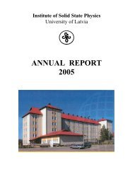
Annual Report 2012 - Latvijas Universitātes Cietvielu fizikas institūts
Annual Report 2012 - Latvijas Universitātes Cietvielu fizikas institūts
Annual Report 2012 - Latvijas Universitātes Cietvielu fizikas institūts

You also want an ePaper? Increase the reach of your titles
YUMPU automatically turns print PDFs into web optimized ePapers that Google loves.
LABORATORY OF SEMICONDUCTOR OPTOELECTRONICS<br />
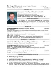
Head of Laboratory Dr. phys. B.Polakovs<br />
Research Area and Main Problems<br />
1. Laser processing of amorphous hydrogenised silicon thin films for solar cell<br />
applications. Investigation of effects of pulsed laser processing on electric,<br />
structural, morphological and photoconductive properties of a-Si:H films.<br />
Development of solar cell prototypes. Scientific cooperation with semiconductor<br />
joint stock company Alfa.<br />
2. Laser scribing and laser processing of graphite, graphene and graphene oxide,<br />
advanced methods of graphene printing on solid substrates. Optical microscopy,<br />
Atomic force microscopy and Scanning Electron microscopy investigation of<br />
printed graphene structures.<br />
3. Synthesis of metal and semiconductor nanocrystals for photonic and solar cell<br />
applications. Investigation of optical, electrical and photoconductive properties<br />
of nanocrystals thin films. Development of nanocrystals based solar cell and<br />
hybrid nanocrystals-polymer solar cell prototypes.<br />
4. MOCVD synthesis of group III-nitrides for photonic and electronic applications.<br />
Investigation of structure and morphology (XRD, RHEED, SEM, AFM).<br />
Investigation of electronic processes using stationary and time-resolved nanoand<br />
picosecond UV-VIS spectroscopy.<br />
5. Controlled manipulations of 1D and 0D nanostructures inside Scanning Electron<br />
Microscope. Investigation of tribological aspects of nanostructures manipulation<br />
(adhesion, static, kinetic friction), nanoindentation experiments, mechanical<br />
characterization (Young modulus, bending strength and yield strength) of<br />
semiconducting and metallic nanowires. Scientific cooperation with Institute of<br />
Physics (University of Tartu) and Estonian Nanotechnology Competence Centre.<br />
Scientific Staff<br />
Prof., Dr. habil. phys. I. Tale<br />
Dr. phys. J. Butikova<br />
Dr. phys. L. Dimitrocenko<br />
Dr. phys. P. Kulis<br />
Dr. phys. B. Polyakov<br />
Mg. phys. J. Jansons<br />
PhD Students<br />
Mg. phys. Guntis Marcins<br />
Mg. phys. Andris Voitkans<br />
Students<br />
Edgars Butanovs<br />
Julija Pervenecka<br />
Cooperation<br />
Latvia<br />
Institute of Biomedical Engineering and Nanotechnologies, Riga Technical University<br />
G. Liberts Innovative Microscopy Center, University of Daugavpils<br />
Joint stock company “Alfa”<br />
Germany<br />
University of Rostock, Rostock<br />
Company “Aixtron”, Achen<br />
Max Plank Institute of Plasma Physics, Garching<br />
Estonia<br />
Institute of Physics, University of Tartu<br />
Estonian Nanotechnology Competence Centre, Tartu<br />
22