

2.5D interposers look increasingly like the near term ... - I-Micronews
2.5D interposers look increasingly like the near term ... - I-Micronews
2.5D interposers look increasingly like the near term ... - I-Micronews

You also want an ePaper? Increase the reach of your titles
YUMPU automatically turns print PDFs into web optimized ePapers that Google loves.
M A Y 2 0 1 2 I S S U E N ° 2 3<br />
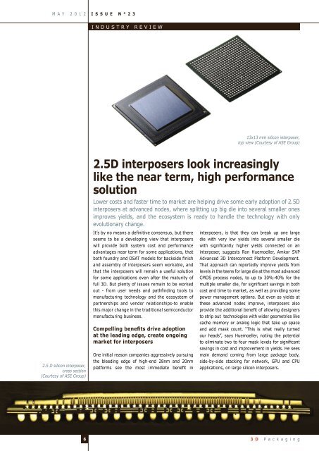
2.5 D silicon interposer,<br />
cross section<br />
(Courtesy of ASE Group)<br />
6<br />
INDUSTRY REVIEW<br />
13x13 mm silicon interposer,<br />
top view (Courtesy of ASE Group)<br />
<strong>2.5D</strong> <strong>interposers</strong> <strong>look</strong> <strong>increasingly</strong><br />
<strong>like</strong> <strong>the</strong> <strong>near</strong> <strong>term</strong>, high performance<br />
solution<br />
Lower costs and faster time to market are helping drive some early adoption of <strong>2.5D</strong><br />
<strong>interposers</strong> at advanced nodes, where splitting up big die into several smaller ones<br />
improves yields, and <strong>the</strong> ecosystem is ready to handle <strong>the</strong> technology with only<br />
evolutionary change.<br />
It’s by no means a defi nitive consensus, but <strong>the</strong>re<br />
seems to be a developing view that <strong>interposers</strong><br />
will provide both system cost and performance<br />
advantages <strong>near</strong> <strong>term</strong> for some applications, that<br />
both foundry and OSAT models for backside fi nish<br />
and assembly of <strong>interposers</strong> seem workable, and<br />
that <strong>the</strong> <strong>interposers</strong> will remain a useful solution<br />
for some applications even after <strong>the</strong> maturity of<br />
full 3D. But plenty of issues remain to be worked<br />
out - from user needs and pathfi nding tools to<br />
manufacturing technology and <strong>the</strong> ecosystem of<br />
partnerships and vendor relationships-to enable<br />
this major change in <strong>the</strong> traditional semiconductor<br />
manufacturing business.<br />
Compelling benefi ts drive adoption<br />
at <strong>the</strong> leading edge, create ongoing<br />
market for <strong>interposers</strong><br />
One initial reason companies aggressively pursuing<br />
<strong>the</strong> bleeding edge of high-end 28nm and 20nm<br />
platforms see <strong>the</strong> most immediate benefi t in<br />
<strong>interposers</strong>, is that <strong>the</strong>y can break up one large<br />
die with very low yields into several smaller die<br />
with signifi cantly higher yields connected on an<br />
interposer, suggests Ron Huemoeller, Amkor SVP<br />
Advanced 3D Interconnect Platform Development.<br />
That approach can reportedly improve yields from<br />
levels in <strong>the</strong> teens for large die at <strong>the</strong> most advanced<br />
CMOS process nodes, to up to 30%-40% for <strong>the</strong><br />
multiple smaller die, for signifi cant savings in both<br />
cost and time to market, as well as providing some<br />
power management options. But even as yields at<br />
<strong>the</strong>se advanced nodes improve, <strong>interposers</strong> also<br />
provide <strong>the</strong> additional benefi t of allowing designers<br />
to strip out technologies with wider geometries <strong>like</strong><br />
cache memory or analog logic that take up space<br />
and add mask count. “This is what really turned<br />
our heads”, says Huemoeller, noting <strong>the</strong> potential<br />
to eliminate two to four mask levels for signifi cant<br />
savings in cost and improvement in yields. He sees<br />
main demand coming from large package body,<br />
side-by-side stacking for network, GPU and CPU<br />
applications, on large silicon <strong>interposers</strong>.<br />
3 D P a c k a g i n g
Altera CoWoS wafer developed with TSMC,<br />
and an image of <strong>the</strong> Altera <strong>2.5D</strong> device using<br />
<strong>the</strong> process (Courtesy of Altera)<br />
Perhaps it’s signifi cant that <strong>the</strong> big industry<br />
leading IDMs Intel, IBM and Samsung, who<br />
were talking about this technology openly a<br />
while ago, now have little to say, though <strong>the</strong>y<br />
clearly have a lot of inside activity going on. “It’s<br />
a good sign that everyone is going silent,” says<br />
Tarun Verma, Altera Corp. Senior Director of<br />
Packaging Engineering. “We’re moving beyond<br />
pre-competitive path fi nding, and everyone is<br />
now working on <strong>the</strong>ir own solutions.”<br />
“We believe that perhaps <strong>the</strong> time for silicon<br />
<strong>interposers</strong> has come,” says Bill Chen, ASE<br />
Fellow and Senior Technical Advisor, noting<br />
that it is becoming <strong>the</strong> top topic at ongoing<br />
industry events. With growing consensus<br />
that wide I/O memory stack with TSV will<br />
become available, <strong>the</strong> technical debate<br />
<strong>increasingly</strong> centers on which applications<br />
are right for 3D and for <strong>2.5D</strong>, ra<strong>the</strong>r than<br />
whe<strong>the</strong>r <strong>the</strong>re is room for both. “The silicon<br />
interposer is now a concept that people think<br />
can be implemented – it won’t be easy, but it<br />
is doable,” he notes. “It’s suffi ciently similar<br />
to <strong>the</strong> old idea of multichip modules that<br />
it’s not such foreign a concept.” Historically,<br />
multichip modules were manufactured by one<br />
company, so <strong>the</strong> idea of combining different<br />
die from different makers was hard to accept,<br />
and to implement. However, this is no longer<br />
such a diffi cult concept today for <strong>the</strong> fablessfoundry-OSAT<br />
community. Back <strong>the</strong>n, test<br />
and rework posed major challenges, and both<br />
remain key challenges for <strong>the</strong> 3D and <strong>2.5D</strong><br />
manufacturing community today. Cost also is<br />
a top consideration, and inevitably <strong>the</strong>re are<br />
major challenges associated with that too. For<br />
high volume manufacturing, an accelerated<br />
learning curve and yield success will be key<br />
to driving down systems cost.<br />
3 D P a c k a g i n g<br />
The most important advantage of <strong>interposers</strong><br />
is <strong>the</strong> ability to mix and match capabilities<br />
on <strong>the</strong> interposer, to build <strong>the</strong> different<br />
functions (processor, memory, analog,<br />
RF, etc) each in <strong>the</strong>ir own optimum silicon<br />
technology and <strong>the</strong>n combine <strong>the</strong>m, instead<br />
of integrating <strong>the</strong>m all in a SoC, argues Matt<br />
Nowak, Qualcomm Senior Director, Advanced<br />
Technology. “However, quantifi cation and<br />
optimization of <strong>the</strong> benefi ts require detailed<br />
‘pathfi nding’ analysis of specifi c product<br />
architecture/technology combinations,” he<br />
notes. The highest tiers of performance will<br />
adopt <strong>the</strong> technology fi rst, where cost is not<br />
a factor if advantages in form factor, signal<br />
integrity and power savings are realized,<br />
he concurs, pointing to computer servers,<br />
network processors, FPGAs, and high<br />
performance graphics. And <strong>interposers</strong> will<br />
remain <strong>the</strong> best ongoing solution for some<br />
high-end functions in computer and network<br />
processing, where <strong>the</strong> signal and power<br />
benefi ts cannot be achieved with o<strong>the</strong>r<br />
existing technology.<br />
Huemoeller expects interposer technology<br />
to move down to <strong>the</strong> core mainstream chip<br />
markets for desktops, tablets and TVs,<br />
because <strong>the</strong> main high volume chip makers<br />
will fi nd <strong>the</strong> direct integration of logic and<br />
memory on wide I/O <strong>interposers</strong> will be<br />
<strong>the</strong> lowest cost solution at <strong>the</strong> system<br />
I S S U E N ° 2 3 M A Y 2 0 1 2<br />
level for <strong>the</strong> logic/memory interface to<br />
reduce latency and reduce <strong>the</strong> power usage<br />
of driving memory. The next generation<br />
above 8000 pin HBM JEDEC memory standard<br />
is targeted at <strong>the</strong> center of <strong>the</strong> market.<br />
Though <strong>the</strong> interposer will add cost, it will<br />
ultimately allow <strong>the</strong> opportunity to reduce<br />
both <strong>the</strong> size and <strong>the</strong> number of layers in <strong>the</strong><br />
mo<strong>the</strong>rboard, as well as <strong>the</strong> number of mask<br />
layers at <strong>the</strong> wafer level, for potentially<br />
signifi cant saving at <strong>the</strong> systems level. Even<br />
as full 3D TSV technology develops, high<br />
end logic makers are <strong>like</strong>ly to keep using<br />
<strong>interposers</strong>, as <strong>the</strong>y are reluctant to put <strong>the</strong><br />
big vias into <strong>the</strong>ir leading edge logic chips,<br />
leery of <strong>the</strong> potential issues associated<br />
with low-k delamination and reliability, he<br />
argues.<br />
“Interposer technology will move down<br />
to <strong>the</strong> desktop, tablet & TV markets as integration<br />
of logic and Wide I/O memory is shown to be cost<br />
effective at <strong>the</strong> system level while reducing<br />
<strong>the</strong> latency and power usage driving memory,”<br />
expects Ron Huemoeller, Amkor Technology<br />
FINE-PITCH INTERPOSERS<br />
« System partitioning » <strong>interposers</strong><br />
Two types of <strong>interposers</strong><br />
3D integrated passive devices<br />
The main driver is heterogenous integration,<br />
concurs Verma, who notes that multiple chips<br />
on <strong>interposers</strong> provides lots of capability<br />
in bandwidth expansion for Altera’s long<br />
<strong>term</strong> roadmap, and those of its partner<br />
TSMC, with which it developed its recently<br />
announced 3D test vehicle. “With our focus<br />
on communications infrastructure and high<br />
speed networks, in my view <strong>the</strong> interposer<br />
will continue to have a role even after full 3D<br />
development, especially for high performance<br />
applications. Our next generation product<br />
portfolio will use <strong>interposers</strong> in both catalog<br />
and customer driven products.”<br />
COARSE INTERPOSERS<br />
3D LED silicon submounts<br />
Interposers for CMOS<br />
image sensors<br />
7<br />
MEMS & sensor 3D<br />
capping inteposers<br />
Miscellaneous <strong>interposers</strong><br />
(3D Silicon & Glass Interposers report, July 2012, Yole Développement)
Cost and re-thinking interconnect<br />
ecosystem remain key<br />
challenges<br />
Interposer cost of course still remains a<br />
key challenge in most people’s minds,<br />
but perhaps even more challenging is<br />
re-thinking <strong>the</strong> working of much of <strong>the</strong><br />
traditional package interconnect sector.<br />
“My 10,000 foot view is four big areas of<br />
need,” says Verma. “We have to fi rst fi gure<br />
out what customers want. Then <strong>the</strong>re is<br />
<strong>the</strong> design environment –how to partition<br />
<strong>the</strong> design very early on in product design,<br />
which is very different from what we’re<br />
used to. Then <strong>the</strong>re’s <strong>the</strong> manufacturing<br />
environment. And fi nally <strong>the</strong>re’s enabling<br />
<strong>the</strong> ecosystem, where people will have to<br />
work closely toge<strong>the</strong>r with partners in new<br />
ways. We need early path fi nding for this<br />
infrastructure, for <strong>the</strong> technology and for <strong>the</strong><br />
viable business models at <strong>the</strong> same time…<br />
It will be an exciting two to three years of<br />
change for <strong>the</strong> foundries and <strong>the</strong> OSATs.”<br />
Biggest challenge of all, says Nowak,<br />
remains software partitioning. Cost remains<br />
a major challenge for many applications, as<br />
well as <strong>the</strong> related issues of yield, testing,<br />
and identifying known good <strong>interposers</strong>.<br />
Progress on meeting<br />
some challenges<br />
M A Y 2 0 1 2 I S S U E N ° 2 3<br />
Interposer packaging costs <strong>the</strong>mselves have<br />
come down sharply from fi rst introduction<br />
some 18 months ago when <strong>the</strong>re was only<br />
one manufacturer, and <strong>the</strong> technology<br />
is still only in development. “We <strong>look</strong>ed<br />
at interposer manufacturing costs quite<br />
hard, and de<strong>term</strong>ined customers’ target<br />
pricing could be achieved, both at entry<br />
level volumes and at future high volume<br />
manufacturing, and at everything from<br />
mid-end graphics applications to highend<br />
routers,” says Huemoeller. Of course,<br />
increasing volumes will help, as will<br />
improvements in <strong>the</strong> less mature process<br />
steps, <strong>like</strong> throughput for wafer thinning<br />
and thin wafer handling, and <strong>the</strong> temporary<br />
adhesive cost. He says general reliability for<br />
multiple die on a 100μm thick interposer<br />
with 10μm wide TSVs at 210μm pitch,<br />
logic at 40μm pitch microbumps with 25μm<br />
diameter passed level 4MRT, TC-B 1000<br />
8<br />
cycles, HTS 1000 hours and HAST 110°C,<br />
85% RH 500 hours.<br />
Front end fabs will most <strong>like</strong>ly make<br />
<strong>interposers</strong> for now, since <strong>the</strong>y have <strong>the</strong><br />
depreciated 65nm tool sets, and decades<br />
of experience doing 1-2μm features at<br />
very high yields. However, that doesn’t<br />
mean <strong>the</strong> <strong>interposers</strong> will necessarily need<br />
65nm technology. Those assets are simply<br />
available at present with excess capacity in<br />
some cases. First generation of interposer<br />
products will require 10μm wide vias and<br />
40-50μm μbumps. To be competitive and<br />
hit <strong>the</strong> pricing targets with decent margin,<br />
suppliers will need to leverage depreciated<br />
assets ra<strong>the</strong>r than new investment,<br />
Huemoeller fi gures, and says Amkor has no<br />
plans to do this internally from scratch.<br />
“Our next generation product portfolio will use<br />
<strong>interposers</strong> in both catalog and customer driven<br />
products”, says Tarun Verma, Altera Corp.<br />
TSV production intercepts - Amkor Technology view<br />
Si InterpT + DDR3T + Logic<br />
GPU, CPU (28nm)<br />
Apps ProcessorT + SDR<br />
Smart Phone / Table (28nm)<br />
Memory (DDRT )<br />
Server, Custom Mem.<br />
45 & 32nm<br />
Si InterposerT + Logic<br />
ASIC, FPGA (28nm)<br />
Logic - Backside Metal<br />
Power Amp.<br />
Die with TSV indicated by = T<br />
Interp. Req'd<br />
Production<br />
Since 2010<br />
But <strong>the</strong>re will <strong>like</strong>ly be room for a variety<br />
of <strong>interposers</strong>. “With heterogeneous<br />
integration, <strong>the</strong>re will be a potential market<br />
for <strong>interposers</strong> where <strong>the</strong> requirements<br />
for pitch and L/S are less demanding,<br />
such as within <strong>the</strong> analog and RF mixed<br />
signal arena,” says Chen, noting ASE has<br />
developed its own interposer technology for<br />
such markets.<br />
Still up in <strong>the</strong> air is who will do <strong>the</strong> rest of <strong>the</strong><br />
process, and how. One option being pioneered<br />
Interposer Required for some platforms<br />
Interposer Required<br />
2011 2012 2013 2014 2015<br />
(Courtesy of Amkor Technology)<br />
by TSMC with Altera in its 3D test vehicle<br />
is for <strong>the</strong> foundry to do <strong>the</strong> whole process,<br />
attaching <strong>the</strong> chip to <strong>the</strong> interposer wafer and<br />
<strong>the</strong>n attaching <strong>the</strong> chip-interposer unit to <strong>the</strong><br />
package substrate. This allows for bonding<br />
<strong>the</strong> die to a perfectly fl at interposer surface<br />
before processing, avoids shipping thinned<br />
wafers, and eliminates all <strong>the</strong> vendor interface<br />
issues. But it also necessitates putting<br />
known-good die on untested <strong>interposers</strong>,<br />
until someone can fi gure out how to test <strong>the</strong><br />
passive <strong>interposers</strong>, although <strong>the</strong> mature<br />
process technology used for <strong>interposers</strong> does<br />
have very high yields.<br />
An alternative approach is to ship <strong>the</strong> IC<br />
wafers to <strong>the</strong> OSAT before thinning, and let<br />
<strong>the</strong> OSAT do <strong>the</strong> thinning and passivation,<br />
<strong>the</strong>n attach <strong>the</strong> die to <strong>interposers</strong> already<br />
bonded to package substrates. This also<br />
avoids having to ship thinned wafers, uses<br />
<strong>the</strong> existing infrastructure of assembly<br />
equipment, and allows <strong>the</strong> assembler to<br />
manage with any warpage or o<strong>the</strong>r issues<br />
caused by backside processes, such as<br />
passivation, that can impact assembly.<br />
Huemoeller says Amkor customers so far<br />
are all endorsing this approach of having<br />
<strong>the</strong> OSAT do <strong>the</strong> backside fi nish, so all back<br />
process quality and assembly are clearly <strong>the</strong><br />
responsibility of <strong>the</strong> assembler, after wafer<br />
mapping clearly identifi es any front side<br />
defects.<br />
Chen notes that <strong>the</strong>re is currently no one<br />
single answer for how best to divide <strong>the</strong><br />
work fl ow of backside fi nish and assembly<br />
with <strong>the</strong> <strong>interposers</strong>. “Our market is an<br />
effi cient market, which means <strong>the</strong> most<br />
effi cient solution will prevail,” he says.<br />
3 D P a c k a g i n g
“Certainly, every case will be different, even<br />
with <strong>the</strong> same players involved. In every<br />
case, players all need to <strong>look</strong> at what each<br />
can bring to <strong>the</strong> table and decide on <strong>the</strong><br />
most effi cient way to divide up <strong>the</strong> task.”<br />
“There are advantages to each different<br />
process fl ow, and proponents of both<br />
approaches will <strong>like</strong>ly fi nd a way to make<br />
<strong>the</strong>m happen. Technically both will work,<br />
with collaboration of <strong>the</strong> right parties,”<br />
says Verma. “The data on which is better<br />
changes monthly—it’s a moving target.” He<br />
argues that methods for testing <strong>interposers</strong><br />
are under development, and possibly some<br />
methods developed to test substrates back<br />
in <strong>the</strong> era of multichip modules that were<br />
never much used could be resurrected.<br />
Putting components on in sequence,<br />
starting with <strong>the</strong> cheapest fi rst and doing<br />
in<strong>term</strong>ediate test before putting on <strong>the</strong><br />
more expensive components can also help<br />
avoid wasting known-good die. He fi gures<br />
both foundries and OSATs will ultimately<br />
be involved in parts of <strong>the</strong> interposer<br />
business, leading to economies of scale<br />
and lower cost. And OSATs may fi gure out<br />
how to make relative coarser <strong>interposers</strong><br />
using <strong>the</strong> existing packaging infrastructure<br />
of depreciated back end equipment, which<br />
could have a major impact on costs.<br />
Most of <strong>the</strong> components of <strong>the</strong> technology<br />
are in place, argues Verma, noting that<br />
though <strong>the</strong> EDA infrastructure is still far<br />
behind what’s needed for true 3D design,<br />
current technology is good enough to<br />
enable fi rst generation product. Plenty of<br />
manufacturing technology issues remain<br />
to reduce costs, but at least <strong>the</strong> issues are<br />
fairly clear, with headroom for improvement<br />
in thin wafer handling throughput and<br />
adhesives, testing technology, assembly<br />
of bumps at 40μm pitch and below, and<br />
underfi ll materials. The trend is towards<br />
compression bonding, for its big advantage<br />
of less <strong>the</strong>rmal cycling of <strong>the</strong> materials, which<br />
can particularly impact <strong>the</strong> low-k dielectric<br />
layers, says Huemoeller. But even <strong>the</strong>rmal<br />
compression bonding is not good enough<br />
for <strong>the</strong> increasing number of bumps, argues<br />
Vermaa. There’s a lot of concentrated effort<br />
in developing alternatives, including direct<br />
copper to copper bonding. Copper-copper<br />
bonding has been proven by Ziptronix and<br />
Intel, and will be needed at


