

Virtex-5 FPGA XtremeDSP Design Considerations User Guide - Xilinx
Virtex-5 FPGA XtremeDSP Design Considerations User Guide - Xilinx
Virtex-5 FPGA XtremeDSP Design Considerations User Guide - Xilinx

Create successful ePaper yourself
Turn your PDF publications into a flip-book with our unique Google optimized e-Paper software.
Chapter 1: DSP48E Description and Specifics<br />
different, highly pipelined, DSP application solutions. The other data inputs and the<br />
control inputs can be optionally registered once. Full speed operation is 550 MHz when<br />
using the pipeline registers. More detailed timing information is available in Chapter 2,<br />
“DSP48E <strong>Design</strong> <strong>Considerations</strong>.”<br />
In its most basic form, the output of the adder/subtracter/logic unit is a function of its<br />
inputs. The inputs are driven by the upstream multiplexers, carry select logic, and<br />
multiplier array.<br />
Equation 1-1 summarizes the combination of X, Y, Z, and CIN by the adder/subtracter. The<br />
CIN, X multiplexer output, and Y multiplexer output are always added together. This<br />
combined result can be selectively added to or subtracted from the Z multiplexer output.<br />
Note that the second option is a new feature of the DSP48E slice and is obtained by setting<br />
the ALUMODE to 0001.<br />
Adder/Sub Out = (Z ± (X + Y + CIN)) or (-Z + (X + Y + CIN) –1) Equation 1-1<br />
A typical use of the slice is where A and B inputs are multiplied and the result is added to<br />
or subtracted from the C register. More detailed operations based on control and data<br />
inputs are described in later sections. Selecting the multiplier function consumes both X<br />
and Y multiplexer outputs to feed the adder. The two 43-bit partial products from the<br />
multiplier are sign extended to 48 bits before being sent to the adder/subtracter.<br />
When not using the first stage multiplier, the 48-bit, dual input, bit-wise logic function<br />
implements AND, OR, NOT, NAND, NOR, XOR, and XNOR. The inputs to these<br />
functions are A:B, C, P, or PCIN selected through the X and Z multiplexers, with the Y<br />
multiplexer selecting either all 1s or all 0s depending on logic operation.<br />
The output of the adder/subtracter or logic unit feeds the pattern detector logic. The<br />
pattern detector allows the DSP48E slice to support Convergent Rounding, Counter<br />
Autoreset when a count value has been reached, and Overflow/Underflow/Saturation in<br />
accumulators. In conjunction with the logic unit, the pattern detector can be extended to<br />
perform a 48-bit dynamic comparison of two 48-bit fields. This enables functions such as<br />
A:B NAND C = = 0, or A:B (bit-wise logic) C = = Pattern to be implemented.<br />
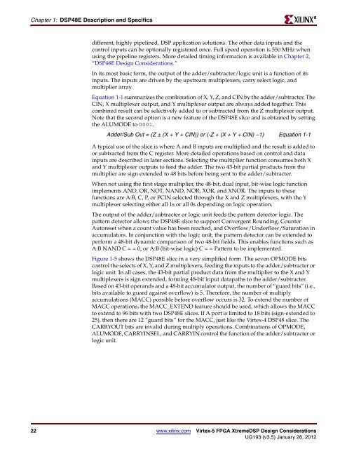
Figure 1-5 shows the DSP48E slice in a very simplified form. The seven OPMODE bits<br />
control the selects of X, Y, and Z multiplexers, feeding the inputs to the adder/subtracter or<br />
logic unit. In all cases, the 43-bit partial product data from the multiplier to the X and Y<br />
multiplexers is sign extended, forming 48-bit input datapaths to the adder/subtracter.<br />
Based on 43-bit operands and a 48-bit accumulator output, the number of “guard bits” (i.e.,<br />
bits available to guard against overflow) is 5. Therefore, the number of multiply<br />
accumulations (MACC) possible before overflow occurs is 32. To extend the number of<br />
MACC operations, the MACC_EXTEND feature should be used, which allows the MACC<br />
to extend to 96 bits with two DSP48E slices. If A port is limited to 18 bits (sign-extended to<br />
25), then there are 12 “guard bits” for the MACC, just like the <strong>Virtex</strong>-4 DSP48 slice. The<br />
CARRYOUT bits are invalid during multiply operations. Combinations of OPMODE,<br />
ALUMODE, CARRYINSEL, and CARRYIN control the function of the adder/subtracter or<br />
logic unit.<br />
22 www.xilinx.com <strong>Virtex</strong>-5 <strong>FPGA</strong> <strong>XtremeDSP</strong> <strong>Design</strong> <strong>Considerations</strong><br />
UG193 (v3.5) January 26, 2012<br />
R


