Amplifier and Data Converter Selection Guide (Rev. B
Amplifier and Data Converter Selection Guide (Rev. B
Amplifier and Data Converter Selection Guide (Rev. B
- No tags were found...

You also want an ePaper? Increase the reach of your titles
YUMPU automatically turns print PDFs into web optimized ePapers that Google loves.
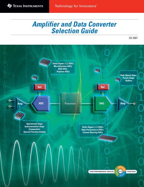
6 <strong>Amplifier</strong>s➔Texas Instruments (TI) offers a wide range ofop amp types including high precision,microPower, low voltage, high voltage, highspeed <strong>and</strong> rail-to-rail in several differentprocess technologies. TI has developed theindustry's largest selection of low-power <strong>and</strong>low-voltage op amps with features designedto satisfy a very wide range of applications.To help facilitate the selection process, aninteractive online op amp parametric searchengine is available at amplifier.ti.com/searchwith links to all op amp specifications.Design ConsiderationsChoosing the best op amp for an applicationinvolves consideration of a variety of interrelatedrequirements. In doing so, designersmust often consider conflicting size, cost <strong>and</strong>performance objectives. Even experiencedengineers can find the task daunting, but itneed not be so. Keeping in mind the followingissues, the choices can quickly be narrowedto a manageable few.Supply voltage (V S )—tables include lowvoltage (< 2.7V min) <strong>and</strong> wide voltage range(> 5V min) sections. Other op amp selectioncriteria (e.g., precision) can be quickly examinedin the supply range column for anappropriate choice. Applications operatingfrom a single power supply may requirerail-to-rail performance <strong>and</strong> considerationof precision-related parameters.Precision—primarily associated with inputoffset voltage (V OS ) <strong>and</strong> its change withrespect to temperature drift, PSRR <strong>and</strong>CMRR. It is generally used to describe opamps with low input offset voltage <strong>and</strong> lowinput offset voltage temperature drift.Precision op amps are required whenamplifying tiny signals from thermocouples<strong>and</strong> other low-level sensors. High-gain ormulti-stage circuits may require lowoffset voltage.Gain b<strong>and</strong>width product (GBW)—the gainb<strong>and</strong>width of a voltage-feedback op ampdetermines its useful b<strong>and</strong>width in anapplication. The maximum available b<strong>and</strong>widthis approximately equal to the gain b<strong>and</strong>widthdivided by the closed-loop gain of the application.For voltage feedback amplifiers, GBW isa constant. Many applications benefit fromchoosing a much wider b<strong>and</strong>width/slew rateop amp to achieve low distortion, excellentlinearity, good gain accuracy, gain flatnessor other behavior that is influenced byfeedback factors.Power (I Q requirements)—a significant issuein many applications. Because op amps canhave a considerable impact on the overallsystem power budget, quiescent current,especially in battery-powered applications,is a key design consideration.Rail-to-rail performance—rail-to-railoutput provides maximum output voltageswing for widest dynamic range. This may beparticularly important with low operatingvoltage where signal swings are limited.Rail-to-rail input capability is often requiredto achieve maximum signal swing in buffer(G = 1) single-supply applications. It can beuseful in other applications, depending onamplifier gain <strong>and</strong> biasing considerations.Voltage noise (V N )—amplifier-generatednoise may limit the ultimate dynamic range,accuracy or resolution of a system. Lownoiseop amps can improve accuracy, even inslow DC measurements.Input bias current (I B )—can create offseterror by reacting with source or feedbackimpedance. Applications with high sourceimpedance or high impedance feedbackelements (such as transimpedance amplifiersor integrators) often require low input biasCommon Op Amp Design QuestionsWhat is the amplitude of theinput signal?To ensure signal errors are small relative tothe input signal, small input signals requirehigh precision (e.g., low offset voltage)amplifiers. Ensure that the amplified outputsignal stays within the amplifieroutput voltage.Will the ambient temperature vary?Op amps are sensitive to temperaturevariations, so it is important to consideroffset voltage drift over temperature.Does the common-mode voltage vary?Make sure the op amp is operatedwithin its common-mode range <strong>and</strong> has anadequate common-mode rejection ratiocurrent. FET-Input <strong>and</strong> CMOS op ampsgenerally provide very low input bias current.Slew rate—the maximum rate of change ofthe amplifier output. It is important whendriving large signals to high frequency. Theavailable large signal b<strong>and</strong>width of an opamp is determined by the slew rateSR/.707(2π)V P .Package size—TI offers a wide variety ofmicroPackages, including WCSP, SOT23,SC70 <strong>and</strong> small, high power-dissipatingPowerPAD packages to meet spacesensitive<strong>and</strong> high-output drive requirements.Many TI single-channel op amps areavailable in SOT23, with some dualamplifiers in SOT23-8.Shutdown mode—an enable/disablefunction that places the amp in a highimpedance state, reducing quiescent currentin many cases to less than 1µA. Allowsdesigners to use wide b<strong>and</strong>width op amps inlower power applications, enabling themonly when they are needed.Decompensated amplifiers—forapplications with gain greater than unitygain (G > 1), decompensated ampsprovide significantly higher b<strong>and</strong>width,improved slew rate <strong>and</strong> lower distortion overtheir unity-gain stable counterparts on thesame quiescent current or noise.(CMRR). Common-mode voltage will induceadditional offset voltage.Does the power supply voltage vary?Power supply variations affect theoffset voltage. This may be especiallyimportant in battery-powered applications.Precision Application Examples• High gain circuits (G > 100)• Measuring small input signals(e.g., from a thermocouple)• Wide operating temperature rangecircuits (i.e., in automotive orindustrial applications)• Single-supply ≤ 5V data-acquisitionsystems where input voltage spanis limited<strong>Amplifier</strong> <strong>and</strong> <strong>Data</strong> <strong>Converter</strong> <strong>Selection</strong> <strong>Guide</strong> Texas Instruments 3Q 2007
<strong>Amplifier</strong>s 7Technology PrimerUnderst<strong>and</strong>ing the relative advantages ofbasic semiconductor technologies will help inselecting the proper device for a specificapplication.CMOS Amps—when low voltage <strong>and</strong>/or lowpower consumption, excellent speed/power ratio,rail-to-rail performance, low cost <strong>and</strong> smallpackaging are primary design considerations,choose microPackaged CMOS amps boastingthe highest precision in the industry.High-Speed Bipolar Amps—when the highestspeed at the lowest power is required, bipolartechnology delivers the best performance.Extremely good power gain gives very highoutput power <strong>and</strong> full power b<strong>and</strong>widths onthe lowest quiescent power. Higher voltagerequirements are also only satisfied in bipolartechnologies.Precision Bipolar Amps—excel in limitingerrors relating to offset voltage. These ampsinclude low offset voltage <strong>and</strong> temperaturedrift, high open-loop gain <strong>and</strong> common-moderejection. Precision bipolar op amps are usedextensively in applications where the sourceOperational <strong>Amplifier</strong> Naming Conventionsimpedance is low, such as a thermocoupleamplifier, <strong>and</strong> where voltage errors, offsetvoltage <strong>and</strong> drift, are crucial to accuracy.Low I B FET Amps—when input impedance isvery high, FET-input amps provide better overallprecision than bipolar-input amps becauseof very low input bias current. Using a bipolaramp in applications with high source impedance(e.g., 500MΩ pH probe), the offset, drift<strong>and</strong> noise produced by bias currents flowingthrough the source would render the circuitvirtually useless. When low current errors arerequired, FET amps provide extremely lowinput bias current, low offset current <strong>and</strong>high input impedance.Dielectrically Isolated FET (Difet ) Amps—Difet processing enables the design ofextremely low input leakage amplifiers byeliminating the substrate junction diodepresent in junction isolated processes. Thistechnique yields very high-precision, lownoiseop amps. Difet processes also minimizeparasitic capacitance <strong>and</strong> output transistorsaturation effects, resulting in improvedb<strong>and</strong>width <strong>and</strong> wider output swing.Op Amp Rapid SelectorThe tables on the following pageshave been subdivided into severalcategories to help quickly narrow thealternatives.Precision Offset Voltage(V OS < 500µV) Pg. 8Low Power(I Q < 500µA) Pg. 9Low Noise(V N ≤ 10nV/ Hz Pg. 10Low Input Bias Current(I B ≤ 10pA) Pg. 11Wide B<strong>and</strong>width, PrecisionGBW > 5MHz Pg. 12Wide Voltage Range(±5 ≤ V S ≤ ±20V) Pg. 13Single Supply(V S (min) ≤ 2.7V) Pg. 14High SpeedBW ≥ 50MHz Pg. 17➔ChannelsSingle = No CharacterDual = 2Triple = 3Quad = 4OPA y 3 63Base Model100 = FET200 = Bipolar300 = CMOS (≤5.5V)400 = High Voltage (>40V)500 = High Power (>200mA)600 = High-Speed (>50MHz)700 = CMOS (12V)800 = High-Speed (>50MHz)Amp ClassTLV = Low Supply VoltageTLC = 5V CMOSTLE = Wide Supply VoltageTLV 278 xChannels <strong>and</strong> Shutdowon Options0 = Single with Shutdown1 = Single2 = Dual3 = Dual with Shutdown4 = Quad5 = Quad with ShutdownAmp ClassTHS = High SpeedTHS x y 01<strong>Amplifier</strong> Type30 = Current Feedback31 = Current Feedback40 = Voltage Feedback41 = Fully Differential42 = Voltage Feedback43 = Fast Voltage Feedback45 = Fully Differential46 = Transimpedance60 = Line Receiver61 = Line Driver73 = Programmable FiltersRecommendedRecommendedSupply Voltage Design Requirements Typical Applications Process TI Amp FamilyV S ≤ 5V Rail-to-Rail, Low Power, Precision, Small Packages Battery Powered, H<strong>and</strong>held CMOS OPA3xx, TLVxxxxV S ≤ 16V Rail-to-Rail, Low Noise, Low Voltage Offset, Precision, Small Packages Industrial, Automotive CMOS OPA3x, TLCxxxx, OPA7xxV S ≤ +3V Low Input Bias Current, Low Offset Current, Industrial, Test Equipment, Optical Networking FET, Difet OPA1xx, OPA627High Input Impedance(ONET), High-End AudioV S ≤ +44V Low Voltage Offset, Low Drift Industrial, Test Equipment, ONET, High-End Audio Bipolar OPA2xx, TLExxxx±5V to ±15V High Speed on Dual Supplies XDSL, Video, Professional Imaging, Difet, High-Speed OPA6xx*, OPA8xx*Dual Supply <strong>Data</strong> <strong>Converter</strong> Signal Conditioning Bipolar, BiCOM THSxxxx*2.7V ≤ V S ≤ 5V High Speed on Single Supply Consumer Imaging, <strong>Data</strong> <strong>Converter</strong> Signal High-Speed CMOS OPA35x, OPA6xx*,Single Supply Conditioning, Safety-Critical Automotive THSxxxx*, OPA8xx**See High-Speed section, Page 15-19Texas Instruments 3Q 2007<strong>Amplifier</strong> <strong>and</strong> <strong>Data</strong> <strong>Converter</strong> <strong>Selection</strong> <strong>Guide</strong>
8<strong>Amplifier</strong>s➔Precision Operational <strong>Amplifier</strong>s1.8V, Zero-Offset, Zero-Drift, Ultra-Low-Power, RRIO, CMOS <strong>Amplifier</strong>sOPA333, OPA2333Get samples, datasheets, <strong>and</strong> app reports at: www.ti.com/OPA333 <strong>and</strong> www.ti.com/sc/device/OPA2333Key Features• Low offset voltage: 10µV (max)• Zero drift: 0.05µV/°C (max)• 0.01Hz to 10Hz noise: 1.1µV PP• Quiescent current: 17µA• Single-supply operation: 1.8V to 5.5V• Rail-to-rail input/output• microSize packages: SC70 <strong>and</strong> SOT23Applications• Temperature measurement• Electronic scales• Medical instrumentation• Battery-powered instruments• H<strong>and</strong>held test equipmentThe OPA333 series of CMOS operational amplifiers are optimized for low-voltage, single-supplyoperation <strong>and</strong> combine TI’s proprietary zero-drift techniques to provide very low offset voltage(10µV max) <strong>and</strong> near-zero drift over time <strong>and</strong> temperature. These miniature, high-precision, lowquiescent current amplifiers offer high-impedance inputs that have a commonmode range100mV beyond the rails <strong>and</strong> rail-to-rail output that swings within 50mV of the rails.RRV EXR 1RR–OPA333++5VR 1V OUTV REFOPA333 low power bridge sensing unit.Low Offset Voltage Operational <strong>Amplifier</strong>s (V OS < 500µV)I Q Per Slew V OS V OS V N atV S V S Ch. GBW Rate (25°C) Drift I B CMRR 1kHz Rail-(V) (V) (mA) (MHz) (V/µs) (mV) (µV/°C) (pA) (dB) (nV/ Hz) Single to-Device Description/Technology Ch. (min) (max) (max) (typ) (typ) (max) (typ) (max) (min) (typ) Supply Rail Package(s) Price *OPAy334/5 Zero-Drift, SHDN, CMOS 1, 2 2.7 5.5 0.35 2 1.6 0.005 0.02 200 110 — Y Out SOT-23, MSOP, SOIC $1.00OPAy734/5 12V, Auto-Zero, SHDN, CMOS 1, 2 2.7 12 0.75 1.6 1.5 0.005 0.01 200 115 110 Y Out SOT-23, SOIC $1.25OPAy333 µPower, Zero Drift, CMOS 1, 2 1.8 5.5 0.025 0.35 0.16 0.01 0.02 200 106 — Y I/O SC-70, SOT-23, SOIC $0.95OPAy277 Precision, Bipolar 1, 2, 4 4 36 0.825 1 0.8 0.02 0.1 1000 130 8 N N SON, SOIC, PDIP $0.85OPA378 Low Power, Wideb<strong>and</strong> 1,2 1.8 5.5 0.100 1 0.5 0.025 0.1 1000 100 15 Y I/O SC70, SOT-23, SOIC $0.95OPAy380 Auto-Zero, 85MHz, TIA, CMOS 1, 2 2.7 5.5 8.8 90 80 0.025 0.03 50 100 110 Y Out MSOP, SOIC, SSOP $1.95OPAy381 Precision, 18MHz, TIA, CMOS 1, 2 2.7 5.5 1 18 12 0.025 0.03 50 100 110 Y Out MSOP, SON $1.45TLC2652A Low Offset, Chopper Stabilized 1 3.8 16 2.4 1.9 3.1 0.001 0.003 100 120 23 N N SOIC $2.20OPAy211 Low Offset Drift, Bipolar 1, 2 4.5 36 3.6 58 27 0.25 0.2 15,000 114 1.1 N Out SOIC, MSOP, SON $3.45OPAy227/28 Low Noise, Bipolar 1, 2, 4 5 36 3.8 8 2.3 0.075 0.1 10000 120 3 N N SOIC, PDIP $1.10OPA827 Precision, FET Input 1, 2 8 36 4.5 18 22 0.25 1 3 108 4.5 N N SOIC, MSOP $5.75TLE2027/37 Wide Supply, Low Noise, Bipolar 1 8 38 5.3 13, 50 2.8, 7.5 0.1 0.4 90000 100 2.5 N N SOIC, PDIP $0.90OPAy234 Low Power, Wide Supply, Bipolar 1, 2, 4 2.7 36 0.3 0.35 0.2 0.1 0.5 25000 96 25 N N MSOP, SOIC $1.05OPA627/37 Ultra-Low THD+N, Difet 1 9 36 7.5 16 55 0.1 0.4 1 106 5.2 N N PDIP, SOIC $12.25OPAy336 µPower, CMOS 1, 2, 4 2.3 5.5 0.032 0.1 0.03 0.125 1.5 10 80 40 Y Out SOT-23, SOIC $0.40OPAy727/8 e-trim, Precision CMOS 1, 2 4 12 4.3 20 30 0.15 0.3 100 86 23 N N MSOP, SON $0.95OPA365 Wideb<strong>and</strong>, Zero-Crossover 1,2 2.2 5.5 5 50 25 0.2 1 10 100 5 Y I/O SOT-23-5,8SOIC $0.95OPAy241 µPower, Bipolar 1, 2, 4 2.7 36 0.03 0.035 0.01 0.25 0.4 20000 80 45 Y Out SOIC, DIP $1.15OPAy251 µPower, ±15V Bipolar 1, 2, 4 2.7 36 0.038 0.035 0.01 0.25 0.5 20000 100 45 Y Out SOIC, DIP $1.15OPA124 Wide B<strong>and</strong>width, Bipolar 1 10 36 3.5 1.5 1.6 0.25 1 1 100 8 N N SOIC $3.95TLC1078 Precision, CMOS 2 1.4 16 0.017 0.085 0.032 0.45 1.1 600 70 68 N N SOIC, DIP $2.30TLV2211 Low Power, 10V, CMOS 1 2.7 10 0.025 0.065 0.025 0.45 0.5 150 70 22 Y Out SOT23 $0.42• Suggested resale price in U.S. dollars in quantities of 1,000.New products are listed in bold red. Preview products are listed in bold blue.<strong>Amplifier</strong> <strong>and</strong> <strong>Data</strong> <strong>Converter</strong> <strong>Selection</strong> <strong>Guide</strong> Texas Instruments 3Q 2007
Ultra-Low-Power, 1µA, RRIO, Zero-Crossover Operational <strong>Amplifier</strong>OPA369<strong>Amplifier</strong>sPrecision Operational <strong>Amplifier</strong>s9➔Get samples, datasheets, <strong>and</strong> app reports at: www.ti.com/sc/device/OPA369Key Features• Ultra-low supply current: 1µA (max)• RRIO Zero-Crossover input topology• Excellent CMRR: 100dB• Low offset voltage: 1mV (max)• Excellent GBW for low power: 10kHz• microPackages: SC70-3, SOT23-3, MSOPApplications• Battery-powered instruments• Portable devices• High impedance applications• Medical instruments• Precision integrators• Test equipmentThe OPA369 family of operational amplifiers combines the TI’s rail-to-rail input/output Zero-Crossover input topology with ultra low power to offer excellent precision to single supplyapplications. Designed with battery powered instrumentation in mind, the OPA369 features1mV offset voltage, 10kHz b<strong>and</strong>width, <strong>and</strong> linear input offset over the entire input rangeof the 1.8V to 5.5V supply range.+1/2OPA2369–C 1CREFR 1 SWR FV CCC 2R B V CCR L–1/2OPA2369+V OUTR 1OPA369 as low-power gas-detection circuit. *Expected release date 3Q 2007.Low-Power Operational <strong>Amplifier</strong>s (I Q < 500µA) <strong>Selection</strong> <strong>Guide</strong>I Q Per Slew V OS Offset V N atV S V S Ch. GBW Rate (mV) Drift I B CMRR 1kHz Rail-(V) (V) (mA) (MHz) (V/µs) (25°C) (µV/°C) (pA) (dB) (nV/ Hz) to-Device Description Ch. (min) (max) (max) (typ) (typ) (max) (typ) (max) (min) (typ) Rail Package(s) Price *TLV240x 2.5V, Sub-µPower, SS, CMOS 1, 2, 4 2.5 16 0.00095 0.0055 0.0025 1.2 3 300 63 — I/O MSOP, PDIP, SOIC, SOT23, TSSOP $0.65TLV224x Low Voltage, 1µA, SS, CMOS 1, 2, 4 2.5 12 0.0012 0.0055 0.002 3 3 500 55 — I/O MSOP, PDIP, SOIC, SOT23, TSSOP $0.60OPA369 Lowest Power, Zero Crossover 1,2 1.8 5.5 0.001 0.01 0.005 1 2 10 100 160 I/O SC70, SOT23 $0.95OPAy349 1µA, SS, CMOS 1, 2 1.8 5.5 0.002 0.07 0.02 10 10 15 52 — I/O SC70, SOIC, SOT23 $0.75OPAy333 µPower, SS, RRIO, Zero-Drift, CMOS 1,2 1.8 5.5 0.025 0.35 0.16 0.01 0.05 200 106 60 I/O SC70, SOT23, SOIC $0.95OPA379 1.8V, Ultra-Low Power, CMOS 1, 2, 4 1.8 5.5 0.005 0.1 0.03 1.5 2.7 50 90 80 I/O SC70, SOT23, SOIC $0.75TLC1078 Low Voltage, Precision, Bipolar 2 1.4 16 0.017 0.085 0.032 0.45 1.1 600 70 68 Out SOIC, PDIP $2.30OPAy241 Bipolar, µPower, High CMRR, 1, 2, 4 2.7 36 0.035 0.35 0.1 0.25 0.4 20000 80 45 Out PDIP, SOIC $1.15OPA703/4 12V, RRIO, General Purpose 1, 2, 4 4 12 0.2 1 0.6 0.75 4 10 70 45 I/O MSOP, SOIC, TSSOP, PDIP $0.40OPAy336 µPower, SS, CMOS 1, 2, 4 2.3 5.5 0.032 0.1 0.03 0.125 1.5 10 80 40 Out SOT23, SOIC $0.40OPAy347 µPower, Low Cost, SS, CMOS 1, 2, 4 2.3 5.5 0.034 0.35 0.17 6 2 10 70 60 I/O SC70, SOT23, SOIC, PDIP $0.48TLV245x µPower, SS, CMOS 1, 2, 4 2.7 6 0.035 0.22 0.12 1.5 0.3 5000 64 51 I/O SOT23, SOIC, PDIP $0.60OPAy251 µPower, Precision, Bipolar 1, 2, 4 2.7 36 0.038 0.035 0.01 0.25 0.5 20000 100 45 Out SOIC, PDIP $1.15OPA378 Wide B<strong>and</strong>width, microPower, e-trim 1, 2 1.8 5.5 0.10 1 0.5 0.025 0.1 1000 100 15 I/O SC70, SOT23, SOIC $0.85OPAy244 µPower, SS, Low Cost, Bipolar 1, 2, 4 2.7 36 0.05 0.24 0.1 1.5 4 25000 84 22 N MSOP, PDIP, SOIC, SOT23, TSSOP $0.55OPAy348 High Open-Loop Gain, SS, CMOS 1, 2, 4 2.1 5.5 0.065 1 0.5 5 2 10 70 35 I/O SC70, SOIC, SOT23, CSP $0.45OPA345 Wideb<strong>and</strong>, Single-Supply 1,2,4 2.7 5.5 0.25 4 4 0.5 2.5 10 80 32 I/O SOT23, SOIC, MSOP $1.20OPA137 Low Cost, FET-Input 1,2,4 4.5 36 0.27 1 3.5 3 15 100 76 45 N SOT23, SOIC, DIP $0.60OPA234 Low Power, Precision 1, 2, 4 2.7 36 0.3 0.35 0.2 0.1 0.5 25000 96 24 N MSOP, SOIC $1.05OPAy334/5 Zero-Drift, Precision, CMOS, SS, SHDN 1, 2 2.7 5.5 0.35 2 0.5 0.005 0.02 200 110 — Out MSOP, SOIC, SOT23 $1.00• Suggested resale price in U.S. dollars in quantities of 1,000.New products are listed in bold red. Preview products are listed in bold blue.Texas Instruments 3Q 2007<strong>Amplifier</strong> <strong>and</strong> <strong>Data</strong> <strong>Converter</strong> <strong>Selection</strong> <strong>Guide</strong>
10 <strong>Amplifier</strong>s➔Precision Operational <strong>Amplifier</strong>s1.1nV/ Hz Noise, Low-Power, Precision Bipolar Operational <strong>Amplifier</strong>OPA211, OPA2211Get samples, datasheets, <strong>and</strong> app reports at: www.ti.com/OPA211 <strong>and</strong> www.ti.com/sc/device/OPA2211Key Features• Low noise voltage: 1.1nV/ Hz at 1kHz• 100nV PP input voltage noise: 0.1Hz to10Hz• Low offset voltage: 100µV (max)• Low offset voltage drift: 0.2µV/°C (typ)• Unity gain b<strong>and</strong>width 58MHz• Wide supply range: ±2.25V to ±18V,+4.5V to +36V• Rail-to-rail output• Output current: 30mA• Shutdown: 20µA (max)Applications• Low-noise signal processing• High-performance ADC drivers• Active filters• Ultrasound amplifiers• Professional audio preamplifiers• Hydrophone amplifiers• MRI <strong>and</strong> CAT ScanLow-Noise Operational <strong>Amplifier</strong>s (V N ≤ 10nV/The OPA211 <strong>and</strong> OPA2211 use proprietary design techniques combined with a high voltageisolated silicon germanium process to deliver outst<strong>and</strong>ing noise performance, (1.1nV/ Hz)precision (100µV) offset voltage <strong>and</strong> wide supply range from 4.5V to 36V single supply operationor ±2.25V to ±18V. Devices have a specified temperature range of –40°C to +125°C <strong>and</strong>operating temperature range of –55°C to +150°C. This performance is available in very smallpackaging 3mm x 3mm 8-pin DFN <strong>and</strong> the 8-pin MSOP.Hz)10Voltage Noise (nV/√Hz3.6mA I Q+15VI Q Per Slew V OS V OS V N atV S V S Ch. GBW Rate (25°C) Drift I B CMRR 1kHz Rail-(V) (V) (mA) (MHz) (V/µs) (mV) (µV/°C) (pA) (dB) (nV/ Hz) Single to-Device Description/Technology Ch. (min) (max) (max) (typ) (typ) (max) (typ) (max) (min) (typ) Supply Rail Package(s) Price *OPAy211 Ultra-Low Noise, 1, 2 8 36 3.6 80 27 0.1 0.2 15000 114 1.1 N N MSOP, SOIC, SON $3.95High PrecisionTLE2027 Wide Supply, Bipolar 1 8 38 5.3 13 2.8 0.1 0.4 90000 100 2.5 N N SOIC $0.90OPA300 Very Wide B<strong>and</strong>width 1 2.7 5.5 12 150 80 2.5 5 5 66 3 Y Out SOT23-6,SOIC-8 $1.25OPA227 High Precision, Bipolar 1, 2, 4 5 36 3.8 8 2.3 0.075 0.1 10000 120 3 N N SOIC, PDIP $1.10OPA228 High Speed, Precision, 1, 2, 4 5 36 3.8 33 10 0.075 0.1 10000 120 3 N N SOIC, PDIP $1.10OPAy827 Ultra-Low THD+N, 1, 2 8 36 4.5 18 22 0.25 1 3 108 4.5 N N MSOP, SOIC $5.75High-PrecisionOPAy350 Excellent ADC Driver, 1, 2, 4 2.7 5.5 7.5 38 22 0.5 4 10 76 5 Y I/O MSOP $0.85OPA365 High Speed, Zero Crossover 1, 2 2.2 5.5 5 50 25 0.5 1 10 100 5 Y I/O SOT-23, SO-8 $0.95OPA353 Good ADC Driver, 1, 2, 4 2.7 5.5 8 44 22 8 5 10 76 5 Y I/O SOT-23, SOIC $1.00Low THD+N, CMOSOPA376 Low Offset, 5MHz 1, 2, 4 2.2 5.5 0.95 5 4 0.05 2 10 80 7.5 Y I/O SC70, SOT23, MSOP, $0.95General PurposeSO8, TSSOPOPA627/37 Precision, High Speed, 1 9 36 7.5 16, 80 55, 135 0.1 0.4 1 106 5.2 N N SOIC $12.25DifetOPA376 Low Power RRIO 1, 2, 4 2.2 55 0.95 5 4 0.05 2 10 80 7.5 Y I/O SC70, SOT23 $0.95OPA121 Precision, Difet S 10 36 4.5 2 2 3 2 5 86 8 N N SOIC-8 $5.10OPAy277 High Precision 1, 2, 4 4 36 0.825 1 0.8 0.02 0.1 1000 130 8 N N SOIC, PDIP $0.85OPA124 Low Noise, Precision, 1 10 36 7.5 1.5 1.6 0.25 2 1 100 8 N N PDIP $3.95BipolarTLC220x Precision, Low Power, 1, 2 4.6 16 1.5 1.8 2.5 0.5 0.5 100 85 8 Y Out SOIC, PDIP $1.65LinCMOSOPAy132 Wide B<strong>and</strong>width, FET-Input 1, 2, 4 4.5 36 4.8 8 20 0.5 2 50 96 8 N N SOIC $1.45* Suggested resale price in U.S. dollars in quantities of 1,000. New products are listed in bold red. Preview products are listed in bold blue.100µV+OPA211_-15V1.1nV/ √Hz200mV1 10 100 1kFrequency (Hz)OPA211 noise density vs. frequency. *Expected Release Date 4Q 2007.<strong>Amplifier</strong> <strong>and</strong> <strong>Data</strong> <strong>Converter</strong> <strong>Selection</strong> <strong>Guide</strong> Texas Instruments 3Q 2007
<strong>Amplifier</strong>sPrecision Operational <strong>Amplifier</strong>s11➔JFET Input, High Precision, Low-Noise Operational <strong>Amplifier</strong>OPA827Get samples, datasheets, <strong>and</strong> app reports at: www.ti.com/sc/device/OPA827Key Features• Ultra-low-input bias current: 3pA• Low Offset: 250µV (max)• Drift: 1µV/°C• Low noise: 4.5nV/ Hz at 1kHz• B<strong>and</strong>width: 18MHz• Packages:• Single: MSOP-8, SO-8• Dual: TSSOP-8, SO-8The OPA827 <strong>and</strong> OPA2827 use proprietary design techniques combined with a high voltageisolated silicon germanium process <strong>and</strong> FET-input transistors to deliver high input impedance(1 x 10 13 Ω), outst<strong>and</strong>ing noise performance, (4.5nV/ Hz) <strong>and</strong> high precision (250µV) offsetvoltage. Devices have specified temperature range of –40°C to +125°C. This performance isavailable in very small, 8-pin MSOP packaging.400nV PP0.1Hz to 10Hz NoiseApplications• Precision ±10V input front-ends• Transimpedance amplifiers• Active filters• ADC drivers• DAC output buffer• High-performance audio200nV PP /Div+15V+5V3.6mA I Q250µVOPA827ADS8505±10VInput1600nV PPClosest Competition–15V1s/Div Frequency (Hz)OPA827 features extremely low noise for data acquisition.*Expected Release Date 4Q 2007.Low Input Bias Current Operational <strong>Amplifier</strong>s (I B ≤ 10pA)I Q Per Slew V OS V OS V N atV S V S Ch. GBW Rate (25°C) Drift I B CMRR 1kHz Rail-(V) (V) (mA) (MHz) (V/µs) (mV) (µV/°C) (pA) (dB) (nV/ Hz) Single to-Device Description/Technology Ch. (min) (max) (max) (typ) (typ) (max) (typ) (max) (min) (typ) Supply Rail Package(s) Price *OPA129 Ultra-Low Bias, Difet 1 10 36 1.8 1 2.5 2 3 0.1 80 17 N N SOIC $3.20OPA124 Low Noise, High Precision 1 10 36 7.5 1.5 1.6 0.25 2 1 100 8 N N PDIP $3.95OPA627/37 Ultra-Low THD+N, Difet 1 9 36 7.5 16, 80 55, 135 0.1 0.4 1 106 5.2 N N PDIP, SOIC $12.25OPAy827 Low Noise, Precision, FET-Input 1, 2 8 36 4.5 18 22 0.25 1 3 108 4.5 N N MSOP, SOIC $5.75OPA344 Low Power, RRIO, SS 1, 2, 4 2.7 5.5 0.25 1 1 0.5 2.5 10 80 32 Y I/O MSOP, DIP, SOIC $0.55OPA363 1.8V, RRIO, High CMRR 1, 2 2.7 5.5 0.75 7 5 0.5 3 10 74 17 Y I/O MSOP, SOIC, SOT23 $0.60OPAy336 SS, µPower, CMOS 1, 2, 4 2.3 5.5 0.032 0.1 0.03 0.125 1.5 10 80 40 Y Out SOT23, SOIC $0.40OPAy340 CMOS, Wide B<strong>and</strong>width 1, 2, 4 2.7 5.5 0.95 5.5 6 0.5 2.5 10 80 25 Y I/O MSOP, SOIC, SOT23, TSSOP $0.80OPAy350 Excellent ADC Driver, Low Noise 1, 2, 4 2.7 5.5 7.5 38 22 0.5 4 10 76 5 Y I/O PDIP, MSOP, SOIC $0.85OPAy365 High Speed, Zero-Crossover, 1, 2 2.2 5.5 5 50 25 0.5 1 10 100 5 Y IN SOT23, SO8 $0.95CMOSOPA376 Low Offset, 5MHz 1, 2, 4 2.2 5.5 0.95 5 4 0.05 2 10 80 7.5 Y I/O SC70, SOT23, MSOP, $0.95SO8, TSSOP* Suggested resale price in U.S. dollars in quantities of 1,000. New products are listed in bold red. Preview products are listed in bold blue.Texas Instruments 3Q 2007<strong>Amplifier</strong> <strong>and</strong> <strong>Data</strong> <strong>Converter</strong> <strong>Selection</strong> <strong>Guide</strong>
12➔<strong>Amplifier</strong>sPrecision Operational <strong>Amplifier</strong>s2.2V, 50MHz, 5nV/ Hz, Zero-Crossover Operational <strong>Amplifier</strong>OPA365Get datasheets at: www.ti.com/OPA365Key Features• Wide b<strong>and</strong>width: 50MHz• High slew rate: 25V/µs• Low noise: 5nV/ Hz• Excellent THD+N: 0.0006%• Low offset: 500µV (max)• High CMRR: 100dB• Rail-to-rail input/output without crossover• Available in single, dual: OPA365, OPA2365• microPackaging: SOT23-5, SO-8, DFN-8Applications• Precision signal conditioning• <strong>Data</strong> acquisition• Process control• Test equipment• Active filters• AudioThe OPA365 is the newest member of the Zero-Crossover family of op amps featuring TI’spatented single-supply, zero-crossover input stage designed to offer excellent performance forvery low-voltage, single-supply ADC applications. These amplifiers are optimized for driving16-bit SAR ADCs <strong>and</strong> feature precision CMRR without the crossover associated with traditionalcomplementary input stages. The input common-mode range includes both the negative <strong>and</strong>positive supplies <strong>and</strong> the output voltage swing is 10mV beyond supply rails. All versions arespecified for operation from –40°C to +125°C. The OPA365 operates on single supplies from2.2V (±1.1V) to 5.5V (±2.25V) <strong>and</strong> features 500µV offset on 5mA supply current.OPA365 designed for 16-bit,single supply acquisition.Wide-B<strong>and</strong>width, Precision Operational <strong>Amplifier</strong>s (GBW > 5MHz)I Q Per Slew V OS V OS V N atV S V S Ch. GBW Rate (25°C) Drift I B CMRR 1kHz Rail-(V) (V) (mA) (MHz) (V/µs) (mV) (µV/°C) (pA) (dB) (nV/ Hz) Single to-Device Description/Technology Ch. (min) (max) (max) (typ) (typ) (max) (typ) (max) (min) (typ) Supply Rail Package(s) Price *TLV2460 Lowest Power, Wide 1, 2, 4 2.7 6 0.575 5.2 1.6 2 2 14000 66 11 Y I/O SOT23-6, PDIP-8, $0.65B<strong>and</strong>widthSOIC-8, TSSOP-8OPAy340 Low Power, CMOS 1, 2, 4 2.7 5.5 0.95 5.5 6 0.5 2.5 10 80 25 Y I/O SOT23, DIP, SOIC $0.80OPA343 General Purpose 1,2,4 2.5 5.5 1.25 5.5 6 3 8 10 74 25 Y I/O SOT23-5, SOIC-8 $0.60OPAy363/4 1.8V, Zero-Crossover, CMOS 1, 2, 4 1.8 5.5 0.75 7 5 0.5 3 10 74 17 Y I/O SOT, SOIC $0.60OPA373 Best Performance/Price 1 2.7 5.5 0.75 6.5 5 3 5 10 80 Y I/O SOT23-6, SOIC-8 $0.36OPA743 Precision, 12V 1,2,4 3.5 12 1.5 7 10 8 7 10 66 30 Y I/O SOT23-5, PDIP-8, $0.95SOIC-8OPAy227 Low Noise, Precision, Bipolar 1, 2, 4 5 36 3.8 8 2.3 0.075 0.1 10000 120 3 N N SOIC $1.10OPAy132 High Speed, FET-Input 1, 2, 4 4.5 36 4.8 8 20 0.5 2 50 96 8 N N SOIC $1.45OPAy227 Low Noise, Bipolar 1, 2, 4 5 36 3.8 8 2.3 0.075 0.1 10000 120 3 N N SOIC, PDIP $1.10TLE2027A Low Noise, Bipolar 1 8 38 5.3 13 2.8 0.025 0.2 90000 11 2.5 N N SOIC, PDIP $1.25OPA627 Precision, High Speed, Difet 1 9 36 7.5 16 55 0.1 0.4 1 106 5.2 N N SOIC, PDIP $12.25OPA381 Precision TIA, CMOS 1 2.7 5.5 1 18 12 0.025 0.03 50 95 110 Y Out MSOP, SON $1.45OPAy827 Ultra-Low THD+N, 1, 2 8 36 4.5 18 22 0.25 1 3 108 4.5 N N MSOP, SOIC $5.75High PrecisionOPA727/8 Precision, e-trim, CMOS 1 4 12 4.3 20 30 0.15 0.3 100 86 10 Y Out MSOP, SON $0.95OPAy228 Precision, Low Noise, 1, 2, 4 5 36 3.8 33 10 0.075 0.1 10000 120 3 N N SOIC, PDIP $1.10OPAy350 Single Supply, Rail-to-Rail, 1, 2, 4 2.7 5.5 7.5 38 22 0.5 4 10 76 5 Y I/O MSOP, SOIC, PDIP $0.85THS4281 Very Low Power RRIO 1 2.7 15 1 80 35 3.5 4 10 12.5 — Y I/O SOT23,MSOP, SOIC $0.95OPA365 High Speed, Zero-Crossover 1, 2 2.2 5.5 5 50 25 0.5 1 10 100 5 Y In SOT23, SOIC-8 $0.95OPAy211 Ultra-Low Noise, 1, 2 8 36 3.6 80 27 0.1 0.2 15000 114 1.1 N N MSOP, SOIC, SON $3.95High PrecisionOPA637 Precision, Decomp, Difet 1 9 36 7.5 80 135 0.1 0.4 1 106 5.2 N N DIP, SOIC $12.25OPAy380 Precision, Wideb<strong>and</strong> TIA 1, 2 2.7 5.5 1 85 80 0.025 0.1 50 100 5 at 1MHz Y Out MSOP, SOIC, SSOP $1.95* Suggested resale price in U.S. dollars in quantities of 1,000. New products are listed in bold red. Preview products are listed in bold blue.<strong>Amplifier</strong> <strong>and</strong> <strong>Data</strong> <strong>Converter</strong> <strong>Selection</strong> <strong>Guide</strong> Texas Instruments 3Q 2007
<strong>Amplifier</strong>s13Wide Voltage Range Operational <strong>Amplifier</strong>s (±5V < V S < ±20V) <strong>Selection</strong> <strong>Guide</strong>Precision Operational <strong>Amplifier</strong>sI Q Per Slew V OS V OS V N atV S V S Ch. GBW Rate (25°C) Drift I B CMRR 1kHz Rail-(V) (V) (mA) (MHz) (V/µs) (mV) (µV/°C) (pA) (dB) (nV/ Hz) Single to-Device Description Ch. (min) (max) (max) (typ) (typ) (max) (typ) (max) (min) (typ) Supply Rail Package(s) Price *TLE214x Widest Supply, Low Noise, High Speed 1, 2, 4 4 44 4.5 5.9 45 0.9 1.7 1500000 85 10.5 N N PDIP, SOIC $0.55TLE202x Low Power, FET-Input 1, 2, 4 4 40 0.3 1.2 0.5 0.6 2 70000 85 17 N N SOIC, TSSOP, PDIP $0.45TLE2027 Excalibur, Low Noise, Bipolar 1 8 38 5.3 13/50 2.8 0.1 0.4 90000 100 2.5 N N SOIC, PDIP $0.90TLE2037 Excalibur, Low Noise, G≥5, Bipolar 1 8 38 5.3 13/50 2.8 0.1 0.4 90000 100 2.5 N N SOIC, PDIP $0.90OPAy241 µPower, Precision, Bipolar 1, 2, 4 2.7 36 0.03 0.035 0.01 0.25 0.4 20000 100 45 Y Out SOIC, PDIP $1.15OPAy251 µPower, Precision, Bipolar 1, 2, 4 2.7 36 0.038 0.035 0.01 0.25 0.5 20000 100 45 Y Out PDIP, SOIC $1.15OPAy244 µPower, Low Cost, Bipolar 1, 2, 4 2.6 36 0.05 0.43 0.1 1.5 4 25000 84 22 N N SOT-23, SOIC, PDIP $0.55OPAy137 Low Cost, FET-Input 1, 2, 4 4.5 36 0.27 1 3.5 3 15 100 76 45 N N SOT23, SOIC $0.60OPAy234 Low Power, Precision, Bipolar 1, 2, 4 2.7 36 0.35 0.35 0.2 0.1 0.5 25000 91 25 N N MSOP, SOIC $1.05OPAy237 Low Cost, Low Power, Bipolar 1, 2 2.7 36 0.35 1.4 0.5 0.75 2 40000 78 28 N N SOT23, SOIC $0.55OPAy130 Low Power, FET-Input 1, 2, 4 4.5 36 0.65 1 2 1 2 20 90 16 N N SOIC $1.40OPAy277 High Precision, Low Power, Bipolar 1, 2, 4 4 36 0.825 1 0.8 0.02 0.1 1000 130 8 N N SON, SOIC $0.85OPAy131 General Purpose, FET-Input 1, 2, 4 9 36 1.75 4 10 0.75 2 50 80 15 N N SOIC $0.75OPAy227 Precision, Low Noise, Bipolar 1, 2, 4 5 36 3.8 8 2.3 0.075 0.1 10000 120 3 N N PDIP, SOIC $1.10OPAy228 Precision, Low Noise, G 5, Bipolar 1, 2, 4 5 36 3.8 33 11 0.075 0.1 10000 120 3 N N PDIP, SOIC $1.10OPAy132 Wide B<strong>and</strong>width, FET-Input 1, 2, 4 4.5 36 4.8 8 20 0.5 2 50 96 8 N N SOIC $1.45OPA124 Low Noise, Precision, Bipolar 1 10 36 7.5 1.5 1.6 0.25 2 1 100 8 N N PDIP $3.95OPA627 Ultra-Low THD+N, Difet 1 9 36 7.5 16 55 0.1 0.4 1 106 5.2 N N PDIP, SOIC $12.25OPA637 Ultra-Low THD+N,G5, Difet 1 9 36 7.5 80 135 0.1 0.4 1 106 5.2 N N PDIP, SOIC $12.25OPAy211 Ultra-Low Noise, High-Precision 1, 2 8 36 3.6 80 27 0.1 0.2 15000 114 1.1 N N MSOP, SOIC, SON $3.95OPAy827 Ultra-Low THD+N, High-Precision 1, 2 8 36 4.5 18 22 0.25 1 3 108 4.5 N N MSOP, SOIC $5.75TLV240x 2.5V, 1µA, Bipolar 1, 2, 4 2.5 16 0.00095 0.0055 0.0025 1.2 3 300 63 800 Y I/O SOT23, SOIC, PDIP $0.65TLV238x Low Power, RRIO, Bipolar 1, 2 2.7 16 0.01 0.16 0.06 6.5 1.1 60 72 90 Y I/O SOT, SOIC, PDIP $0.60TLC220x Precision, Low Noise, Bipolar 1, 2 4.6 16 1.5 1.8 2.5 0.5 0.5 100 85 8 Y Out SOIC, PDIP $1.65TLC08x Low Noise, Wide B<strong>and</strong>width, Bipolar 1, 2, 4 4.5 16 2.5 10 16 1 1.2 50 100 8.5 N N MSOP, SOIC, PDIP $0.45TLV237x 550µA, 3MHz, SHDN 1, 2, 4 2.7 15 0.66 3 2.4 4.5 2 60 57 39 Y I/O SOT23, MSOP $0.43OPAy703/4 12V, Low Power, SHDN, CMOS 1, 2, 4 4 12 0.2 1 0.6 0.75 4 10 70 45 Y I/O MSOP, SOIC, DIP $1.30OPAy734/5 12V, Auto-Zero Precision, SHDN 1, 2 2.7 12 0.75 1.6 1.5 0.005 0.05 200 115 150 Y Out SOT23, SOIC $1.25OPAy743 12V, 7MHz, CMOS 1, 2, 4 3.5 12 1.5 7 10 7 8 10 66 30 Y I/O MSOP, SOIC $0.95OPAy727/8 20MHz, e-trim Precision CMOS 1, 2, 4 4 12 4.3 90 30 0.25 0.3 100 86 23 N N MSOP, SON $0.95OPAy725/6 Very Low Noise, SHDN 1, 2 4 12 5.5 20 30 3 4 200 88 23 Y Out SOT23, SOIC $0.90* Suggested resale price in U.S. dollars in quantities of 1,000. Preview products are listed in bold blue.➔Texas Instruments 3Q 2007<strong>Amplifier</strong> <strong>and</strong> <strong>Data</strong> <strong>Converter</strong> <strong>Selection</strong> <strong>Guide</strong>
14<strong>Amplifier</strong>sPrecision Operational <strong>Amplifier</strong>sSingle-Supply Operational <strong>Amplifier</strong>s V S (min) ≤ 2.7VSlew V OS Offset V N atV S V S I Q Per GBW Rate (25°C) Drift I B CMRR 1kHz Rail-(V) (V) Ch. (MHz) (V/µs) (mV) (µV/°C) (pA) (dB) (nV/ Hz) to-Device Description/Technology Ch. (min) (max) (mA) (typ) (typ) (max) (typ) (max) (min) (typ) Rail Package Price*TLV1078 Single 1.8V RRIO, 8MHz, w/SHDN, CMOS 1, 2, 4 1.4 1.6 0.017 0.085 0.032 0.45 111 800 50 68 Out SOT23, SOIC $2.30OPA349 1µA, Rail-to-Rail, CMOS 1, 2 1.8 5.5 0.002 0.07 0.02 10 10 15 52 — I/O SC70, SOT23, SOIC $0.75OPAy363/4 High CMR,RRIO SHDN, CMOS 1, 2, 4 1.8 5.5 0.75 7 5 0.5 3 10 74 25 I/O SOT23, SOIC $0.60OPA369 Lowest Power, Zero Crossover 1,2 1.8 5.5 0.001 0.01 0.005 1 2 10 100 160 I/O SC70, SOT23 $0.95OPA379 1.8V, Ultra-Low Power, Low Offset, 1, 2, 4 1.8 5.5 0.0045 0.09 0.03 1.5 2.7 50 100 80 I/O SC70, SOT23, SOIC $0.75OPA378 Wide B<strong>and</strong>width microPower e-trim 1,2 1.8 5.5 0.05 1 1 0.1 2 10 90 35 I/O SOT23, MSOP $0.95OPA333 µPower, Zero-Drift, CMOS 1,2 1.8 5.5 0.025 0.35 0.16 0.01 0.05 200 106 130 I/O SC70, SOT23, SOIC $0.95OPA376 Low Offset, 5MHz 1, 2, 4 2.2 5.5 0.95 5 4 0.05 2 10 80 7.5 I/O SC70, SOT23, $0.95MSOP, SO8, TSSOPTLV224x microPower, Lowest supply 1, 2, 4 2.5 12 0.0012 0.0055 0.002 3.0 3.0 500 55 800 I/O SOT23, MSOP, SOIC $0.60TLV237x Precision, Low Power 1, 2, 4 2.7 15 0.66 3 2.4 4.5 2.0 60 50 39 I/O SOT23, MSOP, SOIC $0.47TLV240x Sub 1µA, Low Offset 1, 2, 4 2.5 16 .00095 0.0055 .0025 1.2 3.0 300 63 800 I/O SOT23, MSOP, $0.65SOIC, TSSOPTLV245x Low Offset, General Purpose 1, 2, 4 2.7 6.0 0.035 0.22 0.12 1.5 0.3 5000 70 51 I/O SOT23, MSOP, $0.60SOIC, TSSOPTLV246x Wide B<strong>and</strong>width, Low Noise, Low Power 1, 2, 4 2.7 6.0 0.575 5.2 1.6 1.6 2.0 14000 66 11 I/O SOT23, MSOP, $0.60SOIC, TSSOPTLV247x Low Noise, General Purpose 1, 2, 4 2.7 6.0 0.75 2.8 1.4 2.2 0.4 50 61 15 I/O SOT23, SOIC $0.60TLV248x Low Noise, Low Voltage 1, 2, 4 1.8 3.6 .82 8.0 4.3 3.0 8.0 15 50 18 I/O SOT23, SOIC $0.65OPA348 1MHz, 45µA, RRIO, CMOS 1, 2, 4 2.1 5.5 0.065 1 0.5 5 2 10 70 35 I/O SC70, SOT23, SOIC $0.45OPAy365 High-Speed, Zero-Crossover, CMOS 1, 2 2.2 5.5 5 50 25 0.5 1 10 100 5 In SOT23, SO8 $0.95OPA336 µPower, CMOS 1, 2, 4 2.3 5.5 0.032 0.1 0.03 0.125 1.5 10 80 40 Out SOT23, SOIC $0.40OPA347 Low Power, SC70, CMOS 1, 2, 4 2.3 5.5 0.034 0.35 0.17 6 2 10 70 60 I/O SC70, SOT23, DIP, $0.48SOICOPA343 General Purpose, CMOS 1, 2, 4 2.5 5.5 1.25 5.5 6 8 3 10 74 25 I/O SOT23, SOIC $0.60TLV2770 Single 2.7V High Slew Rate, R/R 1, 2, 4 2.5 5.5 2 4.8 9 2.5 2 100 70 21 Out MSOP, SOIC, DIP $0.70Output, SHDN, CMOSOPA244 µPower, Single-Supply, 1, 2, 4 2.6 36 0.05 0.43 0.1 1.5 4 25000 84 22 In SOT23, SOIC, DIP $0.55Micro<strong>Amplifier</strong> Series, BipolarOPA237 Single-Supply, Micro<strong>Amplifier</strong> 1, 2, 4 2.7 36 0.35 1.4 0.5 0.75 2 40000 78 28 In SOT23, SOIC $0.55Series, BipolarOPA241 Single-Supply, µPower, Bipolar 1, 2, 4 2.7 36 0.03 0.035 0.01 0.25 0.4 20000 80 45 Out SOIC, DIP $1.15OPA300/1 High Speed, Low Noise, SS, CMOS 1 2.7 5.5 12 150 80 5 2.5 5 66 3 Out SOT23, SOIC $1.25OPA334/5 Zero Offset 0.05µV/°C (max), SHDN, CMOS 1, 2 2.7 5.5 0.35 2 1.6 0.005 0.02 200 110 50 Out SOT23 $1.00OPA337 120dB AOL, CMOS Input 1, 2 2.7 5.5 1 3 1.2 3 2 10 74 26 Out SOT23, MSOP, $0.43SOIC, DIPOPA338 Good Speed/Power, G ≥ 5, CMOS 1, 2 2.7 5.5 1 12.5 4.6 3 2 10 74 26 Out SOT23, SOIC $0.43OPA340 5.5MHz, CMOS 1, 2, 4 2.7 5.5 0.95 5.5 6 0.5 2.5 10 80 25 I/O SOT23, SOIC, DIP $0.80OPA341/2 Low Cost, Low Power, CMOS 1, 2, 4 2.7 5.5 1 5.5 6 6 2 10 74 32 I/O SOT23, SOIC $0.75OPA344 Low Power, Low Offset, CMOS 1, 2, 4 2.7 5.5 0.25 1 1 0.5 2.5 10 80 32 I/O SOT23, SOIC, DIP $0.55OPA345 Low Power, Single-Supply, R/R, 1, 2, 4 2.7 5.5 0.25 4 4 0.5 2.5 10 80 32 I/O SOT23, SOIC $0.55Micro<strong>Amplifier</strong> Series, CMOSOPA350 High-Speed, Single-Supply, R/R , CMOS 1, 2, 4 2.7 5.5 7.5 38 22 0.5 4 10 76 5 I/O MSOP, SOIC, DIP $0.85OPA353 Good ADC Driver, Low THD+N, CMOS 1, 2, 4 2.7 5.5 8 44 22 8 5 10 76 5 I/O SOT23, SOIC $1.00OPA373/4 6.5MHz, 585µA, Shutdown, CMOS 1 2.7 5.5 0.75 6.5 5 5 3 10 80 30 I/O SOT23, SOIC $0.36THS4281 High Speed, Low Power 1 2.7 15 1 40 35 3.5 7 10 92 12.5 I/O SOT23, MSOP, SOIC $0.95* Suggested resale price in U.S. dollars in quantities of 1,000. New products are listed in bold red. Preview products are listed in bold blue.<strong>Amplifier</strong> <strong>and</strong> <strong>Data</strong> <strong>Converter</strong> <strong>Selection</strong> <strong>Guide</strong> Texas Instruments 3Q 2007
<strong>Amplifier</strong>s15TI develops high-speed signal conditioningproducts using state-of-the-art processes thatgive leading-edge performance. Used inhigh-speed signal chains <strong>and</strong> analog-to-digitaldrive circuits, high-speed amps are broadlydefined as any amplifier having at least50MHz of b<strong>and</strong>width <strong>and</strong> at least 100V/µsslew rate. High-speed amps from TI come inseveral different types <strong>and</strong> supplyvoltage options.Design ConsiderationsVoltage-feedback type—the mostcommonly used amp <strong>and</strong> the basic buildingblock of most analog signal chains such asgain blocks, filtering, level shifting, buffering,etc. Most voltage-feedback amps are unitygainstable, though some are decompensatedto provide wider b<strong>and</strong>width, faster slew rate<strong>and</strong> lower noise.Current-feedback type—most commonlyseen in video or DSL line driver applications, ordesigns where extremely fast slew rateis needed.Fully differential amplifier (FDA)—the fullydifferential input <strong>and</strong> output topology has theprimary benefit of reducing even orderharmonics, thereby reducing total harmonicdistortion. The FDA also rejects common-modecomponents in the signal <strong>and</strong> provides a largeroutput swing to the load relative to singleendedamplifiers. Fully differential amplifiersare well-suited to driving analog-to-digitalconverters. A V COM pin sets the outputcommon-mode voltage required by newer,single-supply, ADCs.FET-Input (or CMOS) amplifiers—have higherinput impedance than typical bipolar amps<strong>and</strong> are more useful to interfacing to highimpedance sources, such as photodiodes intransimpedance circuits.Video amplifiers—can be used in anumber of different ways, but generally arein the signal path for amplifying, buffering,filtering or driving video lines. The specificationsof most interest are differential gain<strong>and</strong> differential phase. Current-feedbackamps are typically used in video applications,because of their combination of high slewrate <strong>and</strong> excellent output drive at lowquiescent power.High-Speed <strong>Amplifier</strong>sFixed <strong>and</strong> variable gain—these amps haveeither a fixed gain, or a variable gain that canbe set either digitally with a few control pins,or linearly with a control voltage. Fixed-gainamplifiers are fixed internally with gainsetting resistors. Variable gain amplifiers canhave different gain ranges, <strong>and</strong> can also bedifferential input <strong>and</strong>/or output.Packaging—high-speed amplifiers typicallycome in surface-mount packages, becauseparasitics of DIP packages can limit performance.Industry st<strong>and</strong>ard surface-mountpackages (SOIC, MSOP, TSSOP <strong>and</strong> QFN) h<strong>and</strong>lethe highest speed requirements. For b<strong>and</strong>widthsapproaching 1GHz <strong>and</strong> higher, theQFN package decreases inductance <strong>and</strong>capacitance.Evaluation boards—high-speed amps have anassociated fully populated evaluation module(EVM) or an unpopulated printed circuit board(PCB). EVMs are a very important part ofhigh-speed amplifier evaluation, since layout iscritical to design success. To make layoutsimple, Gerber files for the EVMs are available.See page 101 for more information.➔Voltage FeedbackCurrent FeedbackHigh-Speed < 500MHz (GBW Product)THS4001THS4011/4012THS4051/4052THS4081/4082THS4041/4042OPA820/OPA4820OPA2613OPA2614OPA842OPA2652OPA2822THS4271OPA690/2690/3690OPA890/OPA2890OPA2889Fully DifferentialTHS4120/4121THS4130/4131THS4140/4141THS4500/4501THS4502/4503THS4509THS4508THS4511THS4513THS4520FET or CMOS InputOPA656OPA657 (G > 7)OPA355/2355/3355OPA356/2356OPA354/2354/4354OPA357/2357OPA358/OPA360/OPA361OPA300/OPA2300OPA301/OPA2301THS4631OPA380/OPA2380Low Voltage ≤ 3.3VTHS4120/21OPA355/2355/3355OPA356/2356OPA354/2354/4354OPA357/2357OPA300/OPA2300OPA301/OPA2301OPA830/OPA2830/OPA4830OPA832/OPA2832/OPA3832Low Noise ≤ 3nV/ HzTHS4031/4032OPA2822THS4130/4131THS4271OPA300/OPA301OPA820/OPA4820OPA842OPA843 (G > 3)OPA846/OPA2846 (G > 7)OPA847 (G > 12)OPA358OPA820/OPA4820Variable <strong>and</strong> Fixed GainTHS7530VCA2612/2613/2614/2616/2618VCA810VCA8613/VCA8617VCA2615/VCA2617OPA860OPA861BUF602BUF634OPA615OPA693/OPA3693General Purpose+5V to ±5V OperationalOPA683/2683OPA684/2684/3684/4684OPA691/2691/3691OPA692/3692 (G = 2 or ±1)OPA2677THS3201/02OPA694/OPA2694OPA2674General Purpose±5V to ±15V OperationalTHS3112/15THS3122/25THS3110/11THS3120/1THS3091/95THS3092/96THS6184Very High-Speed > 500MHz (GBW Products) Rail-to-Rail Input or OutputOPA843OPA847OPA846/OPA2846THS4271THS4302High-speed amplifiers selection tree.OPA355/2355/3355OPA356/2356THS4222/4226OPA354/2354/4354OPA357/2357OPA358/OPA360/OPA361OPA830/OPA2830/OPA4830OPA832/OPA2832/OPA3832Voltage Limiting OutputOPA698OPA699 (G ≥ 4)Very High-Speed > 500MHzOPA695THS3201/THS3202OPA694/OPA2694Preview devices appear in BLUE.New devices appear in RED.Texas Instruments 3Q 2007<strong>Amplifier</strong> <strong>and</strong> <strong>Data</strong> <strong>Converter</strong> <strong>Selection</strong> <strong>Guide</strong>
16<strong>Amplifier</strong>s➔High-Speed <strong>Amplifier</strong>sLow-Distortion, Fully Differential <strong>Amplifier</strong> with Rail-to-Rail OutputsTHS4520Get samples, datasheets <strong>and</strong> EVMs at: www.ti.com/sc/device/THS4520Key Features• Settling time: 7ns to 0.1% (2V step, G=2V/V,R L = 200Ω)• Slew rate: 570V/µs• Centered input common-mode range• Output common-mode control• Small-signal b<strong>and</strong>width: 450MHz (A V =+2)• Output current: 105mA• Input voltage noise: 2nV/ Hz (f>10kHz)• HD 2 : –115dBc at 100kHz, (8V PP , G=2V/V, R L =1kΩ)• HD 3 : –123dBc at 100kHz, (8V PP , G=2V/V, R L =1kΩ)• Power-down quiescent current: 15µA• Packaging: QFN-16Applications• 5V <strong>and</strong> 3.3V data acquisition systems• High linearity ADC amplifier• Wireless communication• Test <strong>and</strong> measurement• Voice processing systemsSingle <strong>and</strong> Triple 2:1 High-Speed Video MultiplexersOPA875, OPA3875The THS4520 is a fully differential op amp with rail-to-rail output that operates from 3.3V or 5Vsupply. The independent output common-mode control makes it well-suited for dc-coupled,high-accuracy data acquisition systems. With its low distortion, the THS4520 is ideal to driveTI’s industry-leading, 16-bit SAR analog-to-digital converters.500Ω500ΩV i V CM500ΩTHS4520500ΩTHS4520 as differential ADC driver.Get samples, datasheets <strong>and</strong> EVMs at: www.ti.com/sc/device/OPA875 <strong>and</strong> www.ti.com/sc/device/OPA387516-bit SARADCKey Features• Small-signal b<strong>and</strong>width: 700MHz (A V =+2)• B<strong>and</strong>width: 425MHz, 4V PP• Gain flatness: 0.1dB to 200MHz• Channel switching time: 4ns• Switching glitch: 40mV PP• Slew rate: 3100V/µs• Gain accuracy: 2.0V/V ±0.4%• 0.025%/0.025° differential gain/phase• Packaging: SO-8 or MSOP-8(OPA875) or SSOP-16 (OPA3875)Applications• RGB or Y/Pb/Pr video switching• Analog routing switcher• LCD projector input select• High resolution monitors• Broadcast video processing• Triple high speed ADC input muxThe OPA875 <strong>and</strong> OPA3875 are high-speed, very wideb<strong>and</strong>, single-channel <strong>and</strong> triple-channel, 2:1multiplexers. Gain accuracy <strong>and</strong> switching glitch of 40mV PP are improved over earlier solutions using anew (patented) input stage switching approach. System power may be optimized using the enablefeature for the OPA3875. Using this, the OPA3875 powers down to a mere 0.9mA total supply current.The fixed gain-of-2 output stage is ideal for driving double terminated video loads directly. Where asingle channel of the OPA3875 is required, consider the OPA875.RGBChannel 0RGBChannel 175Ω75Ω75Ω75Ω75Ω+5VOPA3875(Patented)75Ω75Ω75ΩRGBOut75ΩOPA3875 functional block diagram.–5V ENChannelSelectRGB Switching<strong>Amplifier</strong> <strong>and</strong> <strong>Data</strong> <strong>Converter</strong> <strong>Selection</strong> <strong>Guide</strong> Texas Instruments 3Q 2007
High-Speed <strong>Amplifier</strong>s <strong>Selection</strong> <strong>Guide</strong><strong>Amplifier</strong>sHigh-Speed <strong>Amplifier</strong>sDistortionSettling THD 1Vpp, G = 2, I QBW BW GBW Time 2Vpp 5MHz Differential PerSupply at A CL G = +2 Product Slew 0.1% G = 1 HD 2 HD 3 V N V OS I B Ch. I OUTVoltage A CL (MHz) (MHz) (MHz) Rate (ns) 1MHz (dBc) (dBc) Gain Phase (nV/ Hz) (mV) (µA) (mA) (mA)Device Ch. SHDN (V) (min) (typ) (typ) (typ) (V/µs) (typ) (dB) (typ) (typ) (typ) (%) (°) (typ) (max) (max) (typ) (typ) Package(s) Price *Voltage Feedback (Sorted by Ascending Gain B<strong>and</strong>width Product)THS4051/52 1, 2 N ±5, ±15 1 70 38 50 240 60 –82 –66 –79 0.01 0.01 14 10 6 8.5 100 SOIC, MSOP PowerPAD $0.95THS4281 1 N +2.7, ±5, +15 1 90 40 — 35 78 — — — 0.05 0.25 12.5 30 0.5 750 30 SOT23-5, MSOP, SOIC $0.95OPA2889 2 Y 5, ±5 1 115 60 75 250 25 –74 –76 –79 0.06 0.04 8.4 5 0.75 0.46 40 MSOP, SOIC $1.20THS4011/12 1, 2 N ±5, ±15 1 290 50 100 310 37 –80 –65 –80 0.006 0.01 7.5 6 6 7.8 110 SOIC, MSOP PowerPAD $1.45THS4081/82 1, 2 N ±5, ±15 1 175 70 100 230 43 –64 –67 –52 0.01 0.05 10 7 6 3.4 85 SOIC, MSOP PowerPAD $1.20OPAy354/57 1, 2, 4 Y 2.5 to 5.5 1 250 90 100 150 30 — –75 –83 0.02 0.09 6.5 8 50pA 4.9 100 SOT23, SOIC PowerPAD $0.75OPAy890 1, 2 Y 5, ±5 1 275 92 120 400 10 –88 –82 –90 0.05 0.03 8 6 1.6 2.25 40 MSOP, SOIC $0.80OPAy830 1, 2 ,4 N +3, +5, ±5 1 310 120 110 600 42 –82 –71 –77 0.07 0.17 9.5 1.5 10 4.25 150 SOT23, SOIC $0.75THS4221/22 1, 2 N 3, 5, ±5, 15 1 230 100 120 975 25 –100 –79 –92 0.007 0.007 13 10 3 14 100 SOIC, MSOP PowerPAD $1.90OPA2613 2 N 5, ±6 1 230 110 125 70 40 –94 — — — — 1.8 1 10 6 350 SOIC, SOIC PowerPAD $1.55OPAy300/301 1 Y 2.7 to 5.5 1 400 80 150 80 30 — –74 –78 0.01 0.1 3 5 0.5 12 40 SOT23, SOIC $1.25OPA842 1 N ±5 1 350 150 200 400 15 –107 –100 –104 0.003 0.008 2.6 1.2 35 20.2 100 SOT23, SOIC $1.55OPA2652 2 N ±5 1 700 200 200 335 — –100 –76 –66 0.05 0.03 8 7 15 5.5 140 SOT23, SOIC $1.15OPAy356 1, 2 N 2.5 to 5.5 1 450 100 200 300 30 — –81 –93 0.02 0.05 5.8 9 50pA 8.3 60 SOT23, SOIC, MSOP $0.70OPAy355 1, 2, 3 Y 2.5 to 5.5 1 450 100 200 300 30 — –81 –93 0.02 0.05 5.8 9 50pA 8.3 60 SOT23, SOIC, MSOP, TSSOP $0.70THS4031/32 1, 2 N ±5, ±15 1 275 100 220 100 60 –72 –77 –67 0.015 0.025 1.6 2 6 8.5 90 SOIC, MSOP PowerPAD $1.65OPA2822 2 N 5, ±5 1 400 200 220 170 32 –96 –81 –91 0.02 0.03 2 1.2 12 4.8 150 SOIC, MSOP $1.35OPA656 1 N ±5 1 400 185 240 290 8 –92 –80 –89 0.01 0.01 6 2 20pA 25 60 SOT23, SOIC $3.35OPA698 1 N 5, ±5 1 450 215 250 1100 — –93 –82 –88 0.012 0.008 5.6 5 10 15.5 120 SOIC $1.90OPAy820 1, 4 N 5 to ±5 1 800 240 280 240 18 –84 –90 –110 0.01 0.03 7.5 0.75 17 5.6 110 SOIC, SOIC PowerPAD $0.90OPA2614 2 N 5, ±6 2 180 180 290 145 35 –85 –72 –81 — — 1.8 1 14.5 6.5 350 SOIC, SOIC PowerPAD $1.55OPAy690 1, 2, 3 Y 5, ±5 1 500 220 300 1800 8 –91 –78 –78 0.06 0.03 5.5 4 8 5.5 190 SOT23, SOIC, SSOP $1.35THS4271/75 1 Y 5, ±5, 15 1 1400 390 400 1000 25 –110 –100 –94 0.007 0.004 3 10 15 22 160 SOIC, MSOP PowerPAD $2.25OPA843 1 N ±5 3 500 — 800 1000 7.5 –105 — — 0.001 0.012 2 1.2 35 20.2 100 SOT23, SOIC $1.60THS4304 1 N 3 to ±5 1 3000 1000 870 1000 5 –92 –92 –75 — — 2.4 4 6 18 100 SOT23, SOIC, MSOP $1.75OPA699 1 N 5, ±5 4 260 — 1000 1400 7 — — — 0.012 0.008 4.1 5 10 15.5 120 SOIC $1.95OPA657 1 N ±5 7 350 — 1600 700 10 — — — — — 4.8 1.8 20pA 14 70 SOT23, SOIC $3.80OPAy846 1, 2 N ±5 7 500 — 1750 625 10 — — — 0.02 0.02 1.2 0.6 19 12.6 80 SOT23, SOIC $1.70OPA847 1 Y ±5 12 600 — 3800 950 10 — — — — — 0.85 0.5 39 18.1 75 SOT23, SOIC $2.00Current Feedback (Sorted by Ascending Gain of +2 B<strong>and</strong>width)THS3110/11 1 Y ±5, ±15 1 100 90 — 1300 27 –78 –60 –61 0.01 0.03 3 6 20 4.8 260 SOIC, MSOP PowerPAD $1.30THS3112/15 2 Y ±5, ±15 1 110 110 — 1550 63 –78 –77 –80 0.01 0.011 2.2 8 23 4.9 270 SOIC, SOIC PowerPAD $2.00THS3120/1 1 Y ±5, ±15 1 130 120 — 1500 11 –53 –65 –53 0.007 0.018 2.5 6 3 7 475 SOIC, MSOP PowerPAD $1.85THS3122/25 2 Y ±5, ±15 1 160 128 — 1550 64 –78 –70 –77 0.01 0.011 2.2 6 23 8.4 440 SOIC, SOIC PowerPAD $2.95OPAy683 1, 2 Y 5, ±5 1 200 150 — 540 — –84 –70 –85 0.06 0.03 4.4 3.5 4 0.94 110 SOT23, SOIC $1.20OPAy684 1, 2, 3, 4 Y 5, ±5 1 210 160 — 820 — –77 –73 –77 0.04 0.02 3.7 3.5 35 1.7 120 SOT23, SOIC, TSSOP $1.35OPA2677 2 N 5, ±6 1 220 200 — 2000 — –87 –75 –85 0.03 0.01 2 4.54 30 9 500 SOIC, SOIC PowerPAD, QFN $1.65THS3091/5 1 Y ±5, ±15 1 235 210 — 5000 42 –72 –79 –88 0.013 0.02 2 3 15 9.5 280 SOIC, SOIC PowerPAD $2.4517➔* Suggested resale price in U.S. dollars in quantities of 1,000. New products are listed in bold red. Preview products are listed in bold blue.Texas Instruments 3Q 2007<strong>Amplifier</strong> <strong>and</strong> <strong>Data</strong> <strong>Converter</strong> <strong>Selection</strong> <strong>Guide</strong>
18➔<strong>Amplifier</strong>sHigh-Speed <strong>Amplifier</strong>sHigh-Speed <strong>Amplifier</strong>s <strong>Selection</strong> <strong>Guide</strong>DistortionSettling THD 1Vpp, G = 2, I QBW BW GBW Time 2Vpp 5MHz Differential PerSupply at A CL G = +2 Product Slew 0.1% G = 1 HD 2 HD 3 V N V OS I B Ch. I OUTVoltage A CL (MHz) (MHz) (MHz) Rate (ns) 1MHz (dBc) (dBc) Gain Phase (nV/ Hz) (mV) (µA) (mA) (mA)Device Ch. SHDN (V) (min) (typ) (typ) (typ) (V/µs) (typ) (dB) (typ) (typ) (typ) (%) (°) (typ) (max) (max) (typ) (typ) Package(s) Price *Current Feedback (Sorted by Ascending Gain of +2 B<strong>and</strong>width) (Continued)THS3092/6 2 Y ±5, ±15 1 235 210 — 5000 42 –72 –79 –88 0.013 0.02 2 4 15 9.5 280 SOIC, SOIC PowerPAD $3.90OPA2674 2 Y 5, ±6 1 250 225 — 2000 — –87 –73 –82 0.03 0.01 2 4.5 30 9 500 SOIC, SOIC PowerPAD $1.70OPAy691 1, 2, 3 Y 5, ±5 1 280 225 — 2100 8 –93 –77 –79 0.07 0.02 1.7 2.5 35 5.1 190 SOT-23, SOIC, SSOP $1.45OPAy694 1, 2 N ±5 1 1500 690 — 1700 13 — –92 –93 0.03 0.015 2.1 4.1 18 5.8 80 SOT-23, SOIC $1.25THS3201/02 1, 2 N ±5, ±7.5 1 1800 850 — 6200 20 –85 –85 –95 0.006 0.03 1.65 3 13 14 115 MSOP, SOT23, SOIC $1.60OPA695 1 Y 5, ±5 1 1700 1400 — 4300 — –86 –88 –95 0.04 0.007 1.8 3 30 12.9 120 SOT23, SOIC $1.35Fully Differential <strong>Amplifier</strong>s (Sorted by Ascending Gain B<strong>and</strong>width Product)THS4130/31 1 Y 5, ±5, ±15 1 150 90 180 52 78 –97 –60 –75 — — 1.3 2 6 12.3 85 SOIC, MSOP PowerPAD $2.80THS4502/03 1 Y 5, ±5 1 370 175 280 2800 6.3 –100 –83 –97 — — 6 7 4.6 23 120 SOIC, MSOP PowerPAD $4.00THS4520 1 Y 3 to 5 1 600 400 1200 520 7 –100 — — — — 2 25 11 13 105 QFN $2.45THS4511 1 Y 3, 5 1 1600 1400 2000 4900 3.3 –97 — — — — 2 5.2 15.5 39.2 61 QFN $3.45THS4513 1 Y 3, 5 1 1600 1400 2000 5100 16 –97 — — — — 2.2 5.2 13 37.7 96 QFN $3.25THS4508 1 Y 3, 5 2 2000 2000 3000 6400 2 –98 — — — — 2.3 5 15.5 39.2 61 QFN $3.95THS4509 1 Y 3, 5 2 2000 2000 3000 6600 2 –98 — — — — 1.9 5 13 37.7 96 QFN $3.75Fixed <strong>and</strong> Variable Gain (Sorted by Ascending A CL B<strong>and</strong>width)VCA810 1 N ±5 0.01 30 30 — 350 30 –35 –71 –35 — — 2.4 0.25 10 20 60 SOIC $5.75OPAy832 1, 2 N 2.8 to ±5 1 90 80 — 350 45 –64 –66 –73 0.1 0.16 9.2 7 10 4.25 120 SOT23, SOIC $0.70BUF634 1 N 5, ±5, ±15 1 180 — — 2000 200 — — — 0.4 0.1 4 100 20 15 250 SOIC $3.05OPAy692 1, 3 Y 5, ±5 1 280 225 — 2000 8 –93 –70 –74 0.07 0.02 1.7 2.5 35 5.1 190 SOT23, SOIC, SSOP $1.15THS7530 1 Y 5 4 300 — — 1750 — –51 –54 –50 — — 1.27 — 30 35 20 TSSOP PowerPAD $3.85BUF602 1 N 3.3, 5, ±5 1 1200 — — 8000 — — — — 0.15 0.04 5.1 30 7 5.8 60 SOT23,SOIC $0.85OPAy693 1 Y 5, ±5 1 1400 700 — 2500 12 –87 –74 –87 0.03 0.01 1.8 2 35 13 120 SOT23, SOIC $1.30THS4303 1 Y 3, 5 10 1800 — — 5500 — — — — — — 2.5 4.25 10 34 180 MSOP PowerPAD $2.10THS4302 1 Y 3, 5 5 2400 — — 5500 — — — — — — 2.8 4.25 10 37 180 MSOP PowerPAD $2.10JFET-Input <strong>and</strong> CMOS <strong>Amplifier</strong>s (Sorted by Ascending Gain B<strong>and</strong>width Product)OPA358 1 Y 2.7 to 3.3 1 100 10 80 55 35 — — — 0.3 0.7 6.4 6 50pA 7.5 50 SC70 $0.45OPAy380 1, 2 N 2.7 to 5.5 1 100 10 90 80 — — — — — — 67 0.025 50pA 7.5 50 MSOP, SOIC $1.95OPAy354 1, 2, 4 N 2.5 to 5.5 1 250 90 100 150 30 — –75 –83 0.02 0.09 6.5 8 50pA 4.9 100 SOT23, SOIC PowerPAD $0.67OPAy357 1, 2 Y 2.5 to 5.5 1 250 90 100 150 30 — –75 –83 0.02 0.09 6.5 8 50pA 4.9 100 SOT23, SOIC PowerPAD $0.67OPAy300/301 1,2 Y 2.7 to 5.5 1 — 80 150 80 30 — –74 –78 0.01 0.1 3 5 5pA 12 40 SOT-23, SOIC $1.25OPAy355 1, 2, 3 Y 2.5 to 5.5 1 450 100 200 300 30 — –81 –93 0.02 0.05 5.8 9 50pA 8.3 60 MSOP $0.69OPAy356 1, 2 N 2.5 to 5.5 1 450 100 200 300 30 — –81 –93 0.02 0.05 5.8 9 50pA 8.3 60 SOT23, SOIC $0.69OPA656 1 N ±5 1 400 185 240 290 8 –92 –80 –89 0.01 0.01 6 2 2pA 25 60 SOT23, SOIC $3.35OPA657 1 N ±5 7 350 — 1600 700 10 –83 –73 –100 — — 4.8 1.8 2pA 14 70 SOT23, SOIC $3.80xDSL Drivers <strong>and</strong> Receivers (Sorted by Ascending Output Current)THS4032 2 N ±5, ±15 1 275 100 220 100 60 –72 –77 –67 0.015 0.025 1.6 2 6 8.5 90 SOIC, MSOP PowerPAD $2.60OPA4684 4 N +5, ±6 1 250 170 — 750 — –79 –80 –80 0.04 0.02 3.7 3.5 35 1.7 120 TSSOP, SOIC $3.30OPA2822 2 N 5, ±5 1 400 200 220 170 32 –96 –81 –91 0.02 0.03 2 1.2 12 4.8 150 SOIC, MSOP $1.35* Suggested resale price in U.S. dollars in quantities of 1,000. New products are listed in bold red.<strong>Amplifier</strong> <strong>and</strong> <strong>Data</strong> <strong>Converter</strong> <strong>Selection</strong> <strong>Guide</strong> Texas Instruments 3Q 2007
<strong>Amplifier</strong>sHigh-Speed <strong>Amplifier</strong>s19➔High-Speed <strong>Amplifier</strong>s <strong>Selection</strong> <strong>Guide</strong>DistortionSettling THD 1Vpp, G = 2, I QBW BW GBW Time 2Vpp 5MHz Differential PerSupply at A CL G = +2 Product Slew 0.1% G = 1 HD 2 HD 3 V N V OS I B Ch. I OUTVoltage A CL (MHz) (MHz) (MHz) Rate (ns) 1MHz (dBc) (dBc) Gain Phase (nV/ Hz) (mV) (µA) (mA) (mA)Device Ch. SHDN (V) (min) (typ) (typ) (typ) (V/µs) (typ) (dB) (typ) (typ) (typ) (%) (°) (typ) (max) (max) (typ) (typ) Package(s) Price *xDSL Drivers <strong>and</strong> Receivers (Sorted by Ascending Output Current) (Continued)THS6022 2 N ±5, ±15 1 210 200 — 1900 70 –75 –55 –58 0.04 0.06 1.7 5 9 7.2 250 TSSOP $2.75OPA2613 2 N 5, ±6 1 230 110 125 70 40 –94 — — 0.01 0.01 1.8 1 10 6 350 SOIC, SOIC PowerPAD $1.55OPA2614 2 N 5, ±6 2 180 180 290 145 35 –75 92 110 — — 1.8 1 14.5 6.5 350 QFN, SOIC, SOIC PowerPAD $1.55THS6184 4 Y ±5, ±16 1 50 — — 400 — –83 –83 –61 — — 2.9 15 15 4.2 400 QFN, TSSOP $3.75OPA2674 2 Y 5, ±6 1 260 — — 2000 — — –82 –93 0.03 0.01 2 2 10 9 500 SOIC $1.70OPA2677 2 N 5, ±6 1 220 200 — 2000 — –87 –75 –85 0.03 0.011 2 4.5 30 9 500 SOIC, SOIC PowerPAD $1.65THS6132 2 Y ±5, ±15 1 80 70 — 300 — –83 –78 –70 — — 3.5 1 1 6.4 500 QFN TQFP PowerPAD $3.95THS6182 2 Y ±5, ±16 1 100 80 — 450 — –88 –72 –70 — — 3.2 20 15 11.5 600 QFN, SOIC PowerPAD $2.95Transimpedance <strong>Amplifier</strong>s (Sorted by Ascending Gain B<strong>and</strong>width Product)OPAy380 1, 2 N 2.7, 5.0 1 90 45 90 80 2000 — — — — — 5.8 0.025 50pA 6.5 50 MSOP, SOIC $1.95OPA656 1 N ±5 1 400 185 240 290 8 –92 –80 –89 0.01 0.01 6 2 20pA 25 60 SOT23, SOIC $3.35OPA657 1 N ±5 7 350 — 1600 700 10 –83 –73 –100 — — 4.8 1.8 20pA 14 70 SOT23, SOIC $3.80OPAy846 1, 2 N ±5 7 500 — 1750 625 10 –105 — — 0.02 0.02 1.2 0.6 19 12.6 80 SOT23, SOIC $1.70OPA847 1 Y ±5 12 600 — 3800 950 10 –110 — — — — 0.85 0.5 39 18.1 75 SOT23, SOIC $2.00Multi-Channel, Fixed-Gain PreampsMPA4609 4 N 5 190 90 — — 150 — — — — — — 0.65 0.2 — 12.5 — TQFP $3.95OPAy875 1, 3 Y ±3 to ±6 2 700 700 — 3100 3 — –69 –90 0.025 0.025 6.7 7 ±18 11 ±70 MSOP, SOIC $1.45OPA4872 1 Y ±3.5 to ±6 1 1100 500 — 2300 14 –75 –62 –86 0.035 0.005 4.5 5 18 10.6 ±75 SOIC $2.15Voltage-Limiting <strong>Amplifier</strong>sOPA698 1 N 5, ±5 1 450 215 250 1100 — –93 –82 –88 0.012 0.008 5.6 5 10 15.5 120 SOIC $1.90OPA699 1 N 5, ±5 4 260 — 1000 1400 — — — — 0.012 0.008 4.1 5 10 15.5 120 SOIC $1.95RF/IF <strong>Amplifier</strong>sTHS9000/1 1 N 3, 5 5.8 500 — — — — — — — — — 0.6 — — Var — MicroMLP, SOT23 $1.05DC Restoration (Sample/Hold <strong>Amplifier</strong>)OPA615 1 N ±5 1 710 — — 2500 — — –62 –47 — — 4.6 4 1 13 5 SOIC, MSOP $4.25Filtered <strong>Amplifier</strong>sTHS7303 3 Y 2.7 to 5.5 — — 9/16/35/ — 40/75/ — –59/–62/ — — 0.13 0.55 — 35 — 6 70 TSSOP $1.65190 155/320 –58/–60THS7313 3 Y 2.7 to 5.5 — — 8 — 35 — –62 — — 0.07 0.12 — 35 — 6 70 TSSOP $1.20THS7314 3 N 2.85 to 5.5 — — 8.5 — 36 — –66 — — 0.1 0.1 — 390 — 5.3 80 SOIC $0.40THS7316 3 N 2.85 to 5.5 — — 36 — 80 — –56 — — 0.1 0.1 — 390 — 5.8 80 SOIC $0.55THS7318 3 Y 2.85 to 5 — — 20 — 80 — –73 — — 0.05 0.03 — — — 3.5 — NanoFree Wafer Scale $3.75THS7327 3 Y 2.7 to 5.5 — — 500 — 1300 — — — — 0.3 0.45 — 65 — 33 80 TQFP $3.35THS7353 3 Y 2.7 to 5.5 — — 9/16/35/ — 40/70/ — –64/–73/ — — 0.15 0.3 — 20 — 5.9 70 TSSOP $1.65150 150/300 –70/–71THS7315 3 Y 2.85 to 5.5 — — 8.5 — 37 — –62 — — 0.2 0.3 — 420 — 5.2 90 SOIC $0.50THS7347 3 Y 2.7 to 5.5 — — 500 — 1300 — –58 — — 0.05 0.1 — 15 — 26.8 80 TQFP $2.75Transconductance <strong>Amplifier</strong>sOPA860 1 N ±5 1 470 — 470 3500 — — –77 –79 — — 2.4 — 5 11.2 15 SOIC $2.25OPA861 1 N ±5 1 80 — 400 900 — — –68 –57 — — 2.4 — 1 5.4 15 SOT23, SOIC $0.95* Suggested resale price in U.S. dollars in quantities of 1,000. New products are listed in bold red.Texas Instruments 3Q 2007<strong>Amplifier</strong> <strong>and</strong> <strong>Data</strong> <strong>Converter</strong> <strong>Selection</strong> <strong>Guide</strong>
20 <strong>Amplifier</strong>s➔Video <strong>Amplifier</strong>sVideo amplifiers—can be used in a numberof different ways, but generally are in thesignal path for amplifying, buffering, filtering ordriving video lines. The specifications of mostinterest for composite video signals, or CVBS,are differential gain <strong>and</strong> differential phase. Forother video signals, such as Y’P’bP’r or RGB,b<strong>and</strong>width – both small signal <strong>and</strong> largesignal, <strong>and</strong> slew rate are of most importance.Noise <strong>and</strong> DC accuracy is also consideredimportant in some high-end applications.The traditional Voltage-Feedback (VFB) amplifiersare widely used because of their ability tobe configured for almost any situation. ManyVFB amplifiers have the ability to accept inputsignals going to the negative rail (or ground),allowing use in many single-supply systems.Additionally, many VFB amplifiers offer rail-torailoutputs offering the widest dynamic rangepossible on small supplies. Traditional VFBamplifiers (non-RRO) designed for video offerthe ability to have very high slew rates, wideb<strong>and</strong>widths, low noise, <strong>and</strong> very good DCcharacteristics. Current-feedback amps arecommonly found in high-end video applications,because of their combination of high slew rate<strong>and</strong> excellent output drive at lowquiescent power.High-Speed Video Multiplexers—Numerous video applications, such as RGB orYPbPr video switching, video routers, highresolution monitors, etc. are creating anincreased need for high-speed switching withmultiplexers (muxes). With the increased needto reduce board space are also the dem<strong>and</strong>sthat these muxes provide low powerconsumption as well as increased functionality,such as the ability to drive 75-Ohms or150-Ohms while maintaining good videoperformance specifications. Thesespecifications include low crosstalk, fastsettling, gain flatness, low switching glitchalong with low differential gain <strong>and</strong> differentialphase. The new OPA875 <strong>and</strong> OPA3875 single<strong>and</strong>triple 2:1 multiplexers along with the newOPA4872, 4:1 multiplexer easily meets theserequirements. Using a new patented inputstage switching approach, the switching glitchis much improved over earlier solutions. Thistechnique uses current steering as the inputswitch while maintaining an overall closedloopdesign.TI brought new technology to the market withthe introduction of the THS7303, THS7313 <strong>and</strong>THS7353. These three-channel devices werethe first to offer full I 2 C programmability of allfunctions independently for each channel,which provides the designer the flexibility toconfigure a video system as required or on-thefly,without the need for hardware upgrades ormodifications. The devices are designed withintegrated Butterworth filters to provide all theanalog signal conditioning required in videoapplications such as set-top boxes, digitaltelevisions, personal video recorders/DVDreaders <strong>and</strong> portable USB devices. These highlyintegrated devices provide space savings as aresult of the high levels of integration <strong>and</strong>advanced package technology.The strong combination of integrated features<strong>and</strong> optimized design make TI’s THS7327 <strong>and</strong>new THS7347, well suited for use in projectors<strong>and</strong> professional video systems. Both3-channel RGBHV video buffers offer a monitorpass-thru amplifier, unity gain buffer, 2:1 inputmux, I 2 C control of all functions on eachchannel, HV synch paths with AdjustableSchmitt Trigger, selectable bias modes <strong>and</strong>rail-to-rail output that swings within 100mV ofthe rails to allow for either AC or DC-coupling.The THS7347 incorporates a 500MHz b<strong>and</strong>width,1200V/µs unity-gain buffer making itideal for driving ADCs <strong>and</strong> video decoders,where the THS7327 offers an integrated 5thorder Butterworth anti-aliasing filter on eachchannel. These filters improve image qualityby eliminating DAC images.Portable Video— Successfully designing ahigh-performance video system into lowvoltage portable applications requires carefulattention to many details. Portableapplications impose very challenging technicalrequirements beyond those required in typicalvideo applications <strong>and</strong> dem<strong>and</strong> particulartrade-offs in performance, power consumption,printed circuit board space <strong>and</strong> cost. A DCcoupledsolution with integrated gain,low-pass filter, level-shifter, <strong>and</strong> shutdownsolves these challenges while maintaininggood video performance <strong>and</strong> eliminates theneed for large, expensive discrete components.The st<strong>and</strong>ard definition (SDTV) THS7314 <strong>and</strong>high definition (HDTV) THS7316 easily meetthese trade-offs by maintaining outst<strong>and</strong>inglow-cost performance while the EDTV/SDTVline driver THS7318, with it’s small profilewafer scale package, is ideal for extremelyboard space sensitive applications.The new low power THS7315 is a fullyintegratedSDTV video amplifier which featuresa rail-to-rail output stage allowing for both AC<strong>and</strong> DC line driving. The low 15.6mA quiescentcurrent at 3.3V makes it an excellent choice forUSB powered or other power sensitive videoapplications.Video <strong>Amplifier</strong>sVoltage FeedbackCurrent Feedback Filtered <strong>Amplifier</strong>s Special FunctionsOPAy354 (2.5V to 5.5V)OPAy355 (2.5V to 5.5V)OPAy356 (2.5V to 5.5V)OPAy357 (2.5V to 5.5V)THS4281 (2.7, ±7.5V)OPAy358 (2.7V to 3.3V)OPA360 (2.7V to 3.3V)OPA361 (2.7V to 3.3V)OPAy830 (2.8V, ±5.0)OPAy832 (2.8V, ±5)OPAy690 (5V, ±5V)OPA842 (5V, ±5V)OPAy820 (5V, ±5V)OPAy694 (±5V)OPAy691 (5V, ±5V)OPAy684 (5V, ±5V)OPAy683 (5V, ±5V)OPAy692 (5V, ±5V)OPAy693 (5V, ±5V)OPAy695 (5V, ±5V)OPA360 (2.7V to 3.3V)OPA361 (2.5V to 3.3V)THS7303 (2.7V to 5.5V)THS7313 (2.7V to 5.5V)THS7353 (2.7V to 5.5V)THS7327 (2.7V to 5.5V)THS7314 (2.85V to 5.5V)THS7315 (2.85V to 5.5V)THS7316 (2.85V to 5.5V)THS7318 (2.85V to 5V)THS7347 (2.7V to 5.5V)OPA615 (±5V)BUF602 (±5V, +5V, +3.3V)OPA861 (±5V)OPAy875 (±5V)OPA4872 (±5V)New devices appear in RED.<strong>Amplifier</strong> <strong>and</strong> <strong>Data</strong> <strong>Converter</strong> <strong>Selection</strong> <strong>Guide</strong> Texas Instruments 3Q 2007
3-Channel RGBHV Video Buffer with I 2 C ControlTHS7327Get samples, datasheets <strong>and</strong> evaluation modules at: www.ti.com/sc/device/THS7327<strong>Amplifier</strong>sVideo <strong>Amplifier</strong>s21➔Key Features• Three video amplifiers for CVBS, S-Video,EDTV, HDTV <strong>and</strong> RGB• HV sync paths with adjustableSchmitt Trigger• 2:1 input MUX• I 2 C control of all functions/all channels• Integrated low-pass filters on ADCbuffer path• Selectable input bias modes• Monitor pass-through functionApplications• Projectors• Digital TVs• Professional video systems• Set-top boxes• DLP ® projectors/televisionsThe THS7327 integrates three analog video channels <strong>and</strong> two digital channels for HV sync,simplifying system design <strong>and</strong> reducing component count. The three analog channelsincorporate unity gain buffering <strong>and</strong> monitor feed-through paths to h<strong>and</strong>le all st<strong>and</strong>ard videoformats, including RGB, YPbPr <strong>and</strong> CVBS. The amplifier’s I 2 C control provides easy systemconfiguration <strong>and</strong> flexibility with programmable functions that include: integrated 2:1 inputmultiplexers which enable switching of multiple video sources; fifth-order anti-aliasing filtersenable use with multiple video st<strong>and</strong>ards; <strong>and</strong> input bias modes.Input 1Input 2THS73270.1µFIn AIn B75Ω0.1µF75Ω2:1DC+ Offset DCSDAAC-BiasSCLX1ACSyncTIPClampBypassLPF9/16/35/75MHzDisable= Open1k Ω 878 Ω3.3V675Ω150Ω0.1µF47µFOut33µFSAG75ΩMonitorOutput3.3V single-supply AC-input/AC-video output system w/SAG correction (1 of 3 channels shown).3.3VADC75Ω3-Channel SDTV Buffer with 5th-Order, Low-Pass Filter Compatible with DaVinci ProcessorsTHS7315Get samples, datasheets, evaluation modules <strong>and</strong> app reports at: www.ti.com/sc/device/THS7315Key Features• 5-pole Butterworth low-pass filterat 8.5MHz• Flexible input configuration• Gain of 5.2V/V (14.3dB) compatible withDaVinci, DM2xx, DM3xx, DM4xx <strong>and</strong>OMAP processors• Low total quiescent current:15.6mA at 3.3V• Rail-to-rail output swings within 100mVfrom the railsApplications• Set-top-box DAC output buffering• DVDR/PVR DAC output buffering• Portable/USB powered systemsTHS7315 is a low-power, single-supply (3V to 5V), 3-channel integrated video buffer. Itincorporates a fifth-order Butterworth filter which can be used as a DAC reconstruction filter oran ADC anti-aliasing filter. The 8.5MHz filter is a perfect choice for SDTV video which includesComposite (CVBS), S-Video, Y’U’V’, G’B’R’(R’G’B’), <strong>and</strong> Y’ P ’BP’ R 480i/576i. Its rail-to-rail outputstage allows for both AC <strong>and</strong> DC line driving.DAC/Encoder(DaVinci)SDTVCVBSS-Video Y’S-Video C’4801/5761Y’P’ B P’ RG’B’R’CVBSY’C’+1.8V500Ω500Ω500Ω+3.3VO1CH.1 IN2 CH.2 INCH.3 IN33VINTHS7315CH.18 OUTCH.2 7OUTCH.3 OUT 6GRN 5GAIN =5.2V/V75Ω75ΩCVBS OUTS-Video75ΩY’OUTC’OUTTHS731575Ω75Ω75Ω3.3V single-supply DaVinci interface with DC output coupled video line driver.Texas Instruments 3Q 2007<strong>Amplifier</strong> <strong>and</strong> <strong>Data</strong> <strong>Converter</strong> <strong>Selection</strong> <strong>Guide</strong>
22<strong>Amplifier</strong>s➔Video <strong>Amplifier</strong>sVideo <strong>Amplifier</strong>s (Sorted by Ascending G = +2 B<strong>and</strong>width)–3dB at 0.1dB I QSupply G = +2 Gain Diff Diff Offset Per Ch. InputVoltage B<strong>and</strong>width Flatness Gain Phase Slew Rate Voltage (mA) RangeDevice Description 1 Ch. SHDN (V) (MHz) (MHz) (%) (°) (V/µs) (mV) (max) (typ) (V) RRO Package(s) Price *THS7313 I 2 C, SD 5th-Order LPF 3 Y 2.7 to 5.5 8 4 0.07 0.12 35 35 6 0 to 2.4 Y TSSOP-20 $1.20THS7314 SDTV, 5th-Order Butterworth 3 Y 2.85 to 5.5 8.5 4.2 0.1 0.1 36 390 5.3 0 to 2.4 Y SOIC $0.40THS7315 SDTV, 5th Order Butterworth, 3 N 2.85 to 5.5 8.5 — 0.2 0.3 37 420 5.2 0 to 0.56 Y SOIC $0.50G = 5.2OPA360 G = 2, DC-Coupled, LPF, 1 Y 2.7 to 3.3 9MHz 5 0.5 1 55 80 6 GND to Y SC-70 $0.49Use with DM270/275/320 2-Pole Filter (V+)–1.5OPA361 G = 5.2, DC-Coupled, LPF, TV 1 Y 2.5 to 3.3 9MHz 5 0.5 1 55 55 5.3 GND to 0.55 Y SC-70 $0.49Detect2-Pole FilterTHS7318 EDTV/SDTV 3 Y 2.85 to 5 20 11 0.05 0.03 80 200 3.5 0 to 2.4 Y Wafer Scale $3.75THS7316 HDTV, 5th Order 3 N 2.85 to 5.5 36 — 0.1 0.1 — 390 5.8 0 to 2.3 Y SOIC $0.55THS4281 Low Power, High Speed, RRIO 1 N +2.7, ±5, +15 40 20 0.05 0.08 35 12.5 750 30 Y SOT, MSOP $0.95OPA358 Small Package, 1 Y 2.7 to 3.3 40 12 0.3 0.7 55 6 5.2 GND –0.1 to Y SC-70 $0.45Low Cost(V+)–1OPAy832 VFB, Fixed Gain 1, 2, 3 N +2.8, ±5 80 — 0.1 0.16 350 7 4.25 –0.5 to 1.5 Y SOT-23, SOIC $0.70OPAy354 VFB, Low Cost 1, 2, 4 N 2.5 to 5.5 100 40 0.02 0.09 150 8 4.9 –0.1 to 5.4 Y SOT-23, SOIC, $0.67MSOP, TSSOPOPAy357 VFB, Low Cost, SHDN 1, 2 Y 2.5 to 5.5 100 40 0.02 0.09 150 8 4.9 –0.1 to 5.4 Y SOT-23, SOIC, $0.67MSOPOPAy830 VFB 1, 2, 4 N +2.8, ±5.5 110 — 0.07 0.17 600 7 4.25 –0.45 to 1.2 Y SO-8, SOT-23 $0.75OPA842 VFB 1 N ±5 150 56 0.003 0.008 400 1.2 20.2 ±3.2 N SOT-23, SOIC $1.55OPAy683 CFB 1, 2 Y ±5, +5 150 37 0.06 0.03 540 1.5 0.9 ±3.75 N SOT-23, SOIC, $1.20MSOPTHS7353 I 2 C, Selectable 3 Y 2.7 to 5.5 9/16/35/ 5/9/20/25 0.15 0.3 40/70/ 20 5.9 0 to 3.4 Y TSSOP-20 $1.65SD/ED/HD/Bypass 150 150/3005th-Order LPF, 0dB GainOPAy684 CFB 1, 2, Y ±5, +5 160 19 0.04 0.02 820 3.5 1.7 ±3.75 N SOT-23, SOIC $1.353, 4THS7303 I 2 C, Selectable 3 Y 2.7 to 5.5 9/16/35/190 5/9.5/ 0.13 0.55 40/75/155/ 35 6 0 to 2.4 Y TSSOP-20 $1.65SD/ED/HD/Bypass 22/125 3205th-Order LPF, 6dBOPAy355 VFB, Low Cost, SHDN 1, 2, Y 2.5 to 5.5 200 75 0.02 0.05 300 9 8.3 –0.1 to 3 Y SOT-23, SOIC, $0.693 MSOP, TSSOPOPAy356 VFB, Low Cost 1, 2 N 2.5 to 5.5 200 75 0.02 0.05 300 9 8.3 –0.1 to 3 Y SOT-23, SOIC, $0.69MSOPOPA656 VFB, JFET-Input 1 N ±5 200 30 0.02 0.05 290 1.8 14 –4/+2.5 N SOT-23, SOIC $3.35OPAy690 VFB 1, 2, 3 Y ±5, +5 220 30 0.06 0.03 1800 4 5.5 ±3.5 N SOT-23, SOIC $1.35OPAy691 CFB 1, 2, 3 Y ±5, +5 225 90 0.07 0.02 2100 2.5 5.1 ±3.5 N SOT-23, SOIC $1.45OPAy820 VFB 1, 4 N ±.5, ±5 230 — 0.01 0.03 240 0.75 5.6 0.9 to 4.5 N SOT-23, SOIC $0.90OPAy692 CFB1, Fixed Gain 1, 3 Y ±5, +5 240 120 0.07 0.02 2000 2.5 5.1 ±3.5 N SOT-23, SOIC $1.15THS7327 RGBHV Buffer, I 2 C, 2:1MUX 3 Y 2.7 to 5.5 9/16/35/ 4/7/15/ 0.3 0.45 1300 65 33 0 to 2.4 Y TQFP-48 $3.3575/500 38/56THS7347 RGBHV Buffer, I 2 C, 2:1MUX 3 Y 2.7 to 5.5 500 350 0.05 0.1 1300 15 26.8 0 to 2.4 Y TQFP-48 $2.75OPAy694 CFB 2 N ±5 690 — 0.03 0.015 1700 4.1 5 ±2.5 N SOT-23, SOIC $1.25OPAy693 CFB, Fixed Gain 1, 3 Y ±5, +5 700 200 0.03 0.01 2500 2 13 ±3.4 N SOT-23, SOIC $1.30OPA695 CFB 1 Y ±5, +5 1400 320 0.04 0.007 4300 3 12.9 ±3.3 N SOT-23, SOIC $1.35BUF602 Closed-Loop Buffer 1 N ±5, N/A 240 0.15 0.04 8000 30 5.8 ±4.0 N SOT-23, SOIC $0.85A V = ±1, 1.4GHz 3.3OPA615 DC Restoration 1 N ±5 N/A N/A N/A N/A 2500 N/A 13 ± 3.5 N SO-14, MSOP $4.25OPA861 Transconductance 1 N ±5 N/A N/A — — 900 12 5.4 ±4.2 N SOT-23, SOIC $0.95Video MultiplexersOPA4872 4:1 MUX 1 Y ±3.5, ±6 500 120 0.035 0.005 2300 5 10.6 ±2.8 N SOIC $2.15OPAy875 2:1 MUX 1, 3 Y ±3, ±6 700 200 0.025 0.025 3100 7 11 ±2.8 N MSOP,SOIC $1.20SSOP, QSOP1 VFB (Voltage Feedback), CFB (Current Feedback) * Suggested resale price in U.S. dollars in quantities of 1,000 New products are listed in bold red.<strong>Amplifier</strong> <strong>and</strong> <strong>Data</strong> <strong>Converter</strong> <strong>Selection</strong> <strong>Guide</strong> Texas Instruments 3Q 2007
<strong>Amplifier</strong>s23Comparator ICs are specialized op ampsdesigned to compare two input voltages <strong>and</strong>provide a logic state output. They can beconsidered one-bit analog-to-digitalconverters.The TI comparator portfolio consists of avariety of products with various performancecharacteristics, including: fast ns responsetime, wide input voltage ranges, extremelylow quiescent current consumption <strong>and</strong> opamp <strong>and</strong> comparator combination ICs.Comparator vs. Op AmpComparator Op AmpSpeed (Response time) Yes NoLogic Output Yes NoWide Diff. Input Range Yes YesLow Offset Drift No YesIn general, if a fast response time is required,use a comparator.Design ConsiderationsOutput topology• Open collector—connects to the logicsupply through a pull-up resistor <strong>and</strong>allows comparators to interface to avariety of logic families.• Push-pull—does not require a pull-upresistor. Because the output swings rail-torail,the logic level is dependent on thevoltage supplies of the comparator.Response time (propagation delay)—applications requiring “near real-time”signal response should consider comparatorswith nanosecond (ns) propagation delay. Notethat as propagation delay decreases, supplycurrent increases. Evaluate what mix ofperformance <strong>and</strong> power can be afforded. TheTLV349x family offers a unique combinationof speed/power with 5µs propagation delayon only 1µA of quiescent current.Combination comparator <strong>and</strong> op amp—forinput signals requiring DC level shifting <strong>and</strong>/orSlower FasterResponse Time Low-to-High (µs)Increasing Speed0.0060.00780.0250.1150.20.311.173680Push-Pull OutputOpen-Drain Output1.41.8LMV331, LMV393, LMV339TLV3491, TLV3492TLC372, TLC374Comparatorsgain prior to the comparator, consider theTLV230x (open drain) or TLV270x (push-pull) opamp <strong>and</strong> comparator combinations. These dualfunction devices save space <strong>and</strong> cost.Comparator <strong>and</strong> voltage reference—comparators typically require a referencevoltage to compare against. The TLV3011is an integrated comparator <strong>and</strong> voltagereference combination in a space-savingSC70 package.TLV3501 S, 12mA/chTL714 S, 12mA/chTL3016 S, 12.5mA/chTL712TLC352, TLC354LM393, LM339TLC393, TLC339TLC3702, TLC3704S, 20mA/chLM211TLV3701, TLV3702, TLV3704TLV3401, TLV3402, TLV3404S, D, Q, 100µA/chS, D, Q, 1.2µA/chD, Q, 150µA/chD, Q, 150µA/chD, Q, 20µA/chD, Q, 20µA/chS, D, Q, 0.8µA/chS, D, Q, 0.55µA/ch3.3 5 16 30Supply Voltage (V)S, 6mA/chD, Q, 500µA/ch➔High-Speed Comparator in SOT23TLV3501Get samples <strong>and</strong> datasheets at: www.ti.com/sc/device/TLV3501Key Features• High speed: 4.5ns response at 20mVoverdrive• Beyond-the-rail common-mode input range• Rail-to-rail, push-pull output• Single-supply operation: 2.7V to 5.5V• Packaging: SOT23Applications• Test <strong>and</strong> measurement• Power supply monitoring• Base stationsThe TLV3501 is a high-speed comparator in a small SOT23 package. Designed for a variety ofapplications, TLV3501 offers very fast response relative to power consumption. It is specifiedover the extended temperature range of –40°C to +125°C.Propagation Delay (ns)987654PROPAGATION DELAY vs. OVERDRIVE VOLTAGEFallRiseV CM = 1VV S = 5VC LOAD = 17pF30 20 40 60 80 100Overdrive Voltage (mV)TLV3501 performancecharacteristics.Texas Instruments 3Q 2007<strong>Amplifier</strong> <strong>and</strong> <strong>Data</strong> <strong>Converter</strong> <strong>Selection</strong> <strong>Guide</strong>
24➔<strong>Amplifier</strong>sComparatorsLow-Power Comparators with Integrated Voltage ReferenceTLV3011, TLV3012Get samples <strong>and</strong> datasheets at: www.ti.com/sc/device/TLV3011 <strong>and</strong> www.ti.com/sc/device/TLV3012Key Features• Comparator <strong>and</strong> voltage reference:• TLV3011: open-drain output• TLV3012: push-pull output• Integrated voltage reference: 1.2V• 1% initial accuracy, 40ppm/°C drift• Low quiescent current: 5µA max• Wide input common-mode range:200mV beyond rails• Propagation delay: 6µs• Very low-voltage operation: 1.8V to 5.5V• Packaging: SC-70 <strong>and</strong> SOT23Applications• Battery voltage monitoring• Power good function• Low signal/voltage detection• Relaxation oscillatorThe TLV3011 is a low-power, open-drain output comparator; the TLV3012 is a push-pull outputcomparator. The integrated 1.242V series voltage reference offers low 100ppm/°C (max) drift,is stable with up to 10nF capacitive load <strong>and</strong> can provide up to 0.5mA (typ) of output current.TLV3011C 110nFV+D IR 11MΩ R PULL-UP(1)10kΩ1.242VTLV301xREFNOTE: (1) Use R PULL-UP with the TLV3011 only.TLV3011 or TLV3012 configured to power-up reset for MSP430.MSP430RESETComparators <strong>Selection</strong> <strong>Guide</strong>I Q Per Output t RESP V OSCh. Current Low-to- V S V S (25°C)(mA) (mA) High (V) (V) (mV)Device Description Ch. (max) (min) (µs) (min) (max) (max) Output Type Package(s) Price*High Speed, t RESP ≤ 0.1µsTLV3501 Ultra-High Speed, Low Power 1, 2 5 20 0.004 2.7 5.5 5 Push-Pull SOT23 $1.50TL714 High Speed, 10mV (typ) Hysteresis 1 12 16 0.006 4.75 5.25 10 Push-Pull PDIP, SOIC $2.16TL3016 High Speed, Low Offset 1 12.5 — 0.0078 5 10 3 Open-Drain/Collector SOIC, TSSOP $0.95TL3116 Ultra Fast, Low Power, Precision 1 14.7 — 0.0099 5 10 3 Open-Drain/Collector SOIC, TSSOP $0.95TL712 Single, High Speed 1 20 16 0.025 4.75 5.25 5 Push-Pull PDIP, SOIC, SOP $0.83LM306 Single, Strobed, General Purpose 1 6.8 100 0.028 –6 12 5 Push-Pull PDIP, SOIC $0.42LM211 Single, High Speed, Strobed 1 6 — 0.115 3.5 30 3 Open-Drain/Collector PDIP, SOIC $0.20LM311 Single, High Speed, Strobed, Differential 1 7.5 — 0.115 3.5 30 7.5 Open-Drain/Collector PDIP, SOIC, SOP, TSSOP $0.18LM111 Single, Strobed, Differential 1 6 — 0.165 3.5 30 3 Open-Drain/Collector CDIP, LCCC $1.37Low Power, I Q < 0.5mATLV3401 Nanopower, Open-Drain, RRIO 1, 2, 4 0.00055 — 80 2.5 16 3.6 Open-Drain/Collector MSOP, PDIP, SOIC, $0.60SOT23, TSSOPTLV3701 Nanopower, Push-Pull, RRIO 1, 2, 4 0.0008 — 36 2.5 16 5 Push-Pull MSOP, PDIP, SOIC, $0.60SOT23, TSSOPTLV3491 Low Voltage, Excellent Speed/Power 1, 2 0.0012 — < 0.1 1.8 5.5 15 Push-Pull SOT23, SOIC, TSSOP $0.42TLV2302 Sub-µPower, Op Amp <strong>and</strong> 1, 2 0.0017 — 55 2.5 16 5 Open-Drain/Collector MSOP, PDIP, SOIC, $0.90Comparator, RRIOTSSOPTLV2702 Sub-µPower, Op Amp <strong>and</strong> 1, 2 0.0019 — 36 2.5 16 5 Push-Pull MSOP, PDIP, SOIC, $0.90Comparator, RRIOTSSOPTLC3702 Dual <strong>and</strong> Quad, µPower 2, 4 0.02 4 1.1 3 16 5 Push-Pull PDIP, SOIC, TSSOP $0.34TLC393 Low Power, LM393 Replacement 2 0.02 6 1.1 3 16 5 Open-Drain/Collector PDIP, SOIC, SOP, TSSOP $0.37*Suggested resale price in U.S. dollars in quantities of 1,000.New products are listed in bold red.<strong>Amplifier</strong> <strong>and</strong> <strong>Data</strong> <strong>Converter</strong> <strong>Selection</strong> <strong>Guide</strong> Texas Instruments 3Q 2007
<strong>Amplifier</strong>sComparators <strong>Selection</strong> <strong>Guide</strong> (Continued)25➔I Q Per Output t RESP V OSCh. Current Low-to- V S V S (25°C)(mA) (mA) High (V) (V) (mV)Device Description Ch. (max) (min) (µs) (min) (max) (max) Output Type Package(s) Price*Low Power, I Q < 0.5mA (Continued)TLC339 Quad, Low Power 4 0.02 6 1 3 16 5 Open-Drain/Collector PDIP, SOIC, TSSOP $0.44LP2901 Quad, Low Power, General Purpose 4 0.025 — 1.3 5 30 5 Open-Drain/Collector PDIP, SOIC $0.56LP339 Quad, Low Power, General Purpose 4 0.025 — 1.3 5 30 5 Open-Drain/Collector PDIP, SOIC $0.49LMV393 Dual, Low Voltage 2 0.1 10 0.2 2.7 5.5 7 Open-Drain/Collector SOIC, TSSOP $0.34LMV339 Quad, Low Voltage 4 0.1 — 0.2 2.7 5.5 7 Open-Drain/Collector SOIC, TSSOP $0.36LMV331 Single, Low Voltage 1 0.12 10 0.2 2.7 5.5 7 Open-Drain/Collector SC70, SOT23 $0.34TLC372 Fast, Low Power 2, 4 0.15 6 0.2 2 18 5 Open-Drain/Collector PDIP, SOIC, TSSOP $0.33TLM3302 Quad, General Purpose 4 0.2 6 0.3 2 28 20 Open-Drain/Collector PDIP, SOIC $0.46LP211 Single, Strobed, Low Power 1 0.3 — 1.2 3.5 30 7.5 Open-Drain/Collector SOIC $0.50LP311 Single, Strobed, Low Power 1 0.3 1.6 1.2 3.5 30 7.5 Open-Drain/Collector PDIP, SOIC, SOP $0.46Low Voltage, V S ≤ 2.7V (min)TLC352 1.4V 2, 4 0.15 6 0.2 1.4 18 5 Open-Drain/Collector PDIP, SOIC, TSSOP $0.40TLV3491 Low Voltage, Excellent Speed/Power 1, 2, 4 0.0012 — < 0.1 1.8 5.5 15 Push-Pull SOT23, SOIC, TSSOP $0.42TLV2352 Low Voltage 2, 4 0.125 6 0.2 2 8 5 Open-Drain/Collector PDIP, SOIC, TSSOP $0.90TLC372 Fast, Low Power 2 0.15 6 0.2 2 18 5 Open-Drain/Collector PDIP, SOIC, TSSOP $0.33LM3302 Quad, General Purpose 4 0.2 6 0.3 2 28 20 Open-Drain/Collector PDIP, SOIC $0.46LM2903 Dual, General Purpose 2 0.5 6 0.3 2 30 7 Open-Drain/Collector PDIP, SOIC, SOP, TSSOP $0.22LM293 Dual, General Purpose 2 0.5 6 0.3 2 30 5 Open-Drain/Collector PDIP, SOIC $0.28LM293A Dual, General Purpose 2 0.5 6 0.3 2 30 3 Open-Drain/Collector SOIC $0.36LM393 Dual, General Purpose 2 0.5 6 0.3 2 30 5 Open-Drain/Collector PDIP, SOIC, SOP, TSSOP $0.18LM393A Dual, General Purpose 2 0.5 6 0.3 2 30 3 Open-Drain/Collector PDIP, SOIC, SOP, TSSOP $0.27LM239 Quad, General Purpose 4 0.5 6 0.3 2 30 5 Open-Drain/Collector PDIP, SOIC $0.28LM239A Quad, General Purpose 4 0.5 6 0.3 2 30 2 Open-Drain/Collector SOIC $0.91LM2901 Quad, General Purpose 4 0.625 6 0.3 2 30 3 Open-Drain/Collector PDIP, SOIC, SOP, TSSOP $0.22LM339 Quad, General Purpose 4 0.5 6 0.3 2 30 5 Open-Drain/Collector PDIP, SOIC, SOP, $0.18SSOP, TSSOPLM339A Quad, General Purpose 4 0.5 6 0.3 2 30 3 Open-Drain/Collector PDIP, SOIC, SOP $0.27TL331 Single, Differential 1 0.7 6 0.3 2 36 5 Open-Drain/Collector SOT23 $0.28LM139 Quad 4 0.5 6 0.3 2 36 5 Open-Drain/Collector SOIC $0.54LM139A Quad 4 0.5 6 0.3 2 36 2 Open-Drain/Collector SOIC $0.94LM193 Dual 4 0.5 6 0.3 2 36 5 Open-Drain/Collector SOIC $0.30TLV3401 Nanopower, RRIO 1, 2, 4 0.00055 — 80 2.5 16 3.6 Open-Drain/Collector MSOP, PDIP, SOIC, $0.60SOT23, TSSOPTLV3701 Nanopower, RRIO 1, 2, 4 0.0008 — 36 2.5 16 5 Push-Pull MSOP, PDIP, SOIC, $0.60SOT23, TSSOPLMV331 Single, Low Voltage 1 0.12 10 0.2 2.7 5.5 7 Open-Drain/Collector SC70, SOT23 $0.34LMV393 Dual, Low Voltage 2 0.1 10 0.2 2.7 5.5 7 Open-Drain/Collector SOIC, TSSOP $0.34LMV339 Quad Low-Voltage 4 0.1 — 0.2 2.7 5.5 7 Open-Drain/Collector SOIC, TSSOP $0.36Combination Comparator <strong>and</strong> Op AmpTLV2302 Sub-µPower, Op Amp <strong>and</strong> 2 0.0017 — 55 2.5 16 5 Open-Drain/Collector MSOP, PDIP, SOIC, $0.90Comparator, RRIOTSSOPTLV2702 Sub-µPower, Op Amp <strong>and</strong> 2, 4 0.0019 — 36 2.5 16 5 Push-Pull MSOP, PDIP, SOIC, $0.90Comparator, RRIOTSSOPComparator <strong>and</strong> Voltage ReferenceTLV3011 µPower, Comparator 1 0.003 5 6 1.8 5.5 15 Open-Drain/Collector SC-70, SOT23 $0.75with 1.242V ReferenceTLV3012 µPower, Comparator 1 0.003 5 6 1.8 5.5 15 Push-Pull SC-70, SOT23 $0.75with 1.242V Reference* Suggested resale price in U.S. dollars in quantities of 1,000.Texas Instruments 3Q 2007<strong>Amplifier</strong> <strong>and</strong> <strong>Data</strong> <strong>Converter</strong> <strong>Selection</strong> <strong>Guide</strong>
26 <strong>Amplifier</strong>s➔Difference <strong>Amplifier</strong>sThe difference amplifier is a moderate inputimpedance, closed-loop, fixed-gain block thatallows the acquisition of signals in thepresence of ground loops <strong>and</strong> noise. Thesedevices can be used in a variety of precision,general-purpose, audio, low-power, highspeed<strong>and</strong> high-common-mode voltageapplications.Difference <strong>Amplifier</strong>The basic difference amplifier employs an opamp <strong>and</strong> four on-chip, precision, laser trimmedresistors. The INA132, for example, operateson 2.7V to 36V supplies <strong>and</strong> consumes only160µA. It has a differential gain of 1 <strong>and</strong> highcommon-mode rejection. The output signalcan be offset by applying a voltage to the Refpin. The output sense pin can be connecteddirectly at the load to reduce gain error.Because the resistor network divides downthe input voltages, difference amplifiers canoperate with input signals that exceed thepower supplies.High Common-Mode VoltageDifference <strong>Amplifier</strong> TopologyA five-resistor version of the simpledifference amplifier results in a device thatcan operate with very high levels ofcommon-mode voltage—far beyond itspower supply rails. For example, the INA117can sense differential signals in the presenceof common-mode voltages as high as ±200Vwhile being powered from ±15V. This deviceis very useful in measuring current from ahigh-voltage power supply through a highsideshunt resistor.Design ConsiderationsPower supply—common-mode voltage isalways a function of the supply voltage. TheINA103 instrumentation amplifier is designedto operate on voltage supplies up to ±25V,while the INA122 difference amp can beoperated from a 2.2V supply.Output voltage swing—lower supplyvoltage often drives the need to maximizedynamic range by swinging close to the rails.Should I Use a Difference <strong>Amplifier</strong>or Instrumentation <strong>Amplifier</strong>?Difference amplifiers excel when measuring signals with common-mode voltages greaterthan the power supply rails, when there is a low power requirement, when a small packageis needed, when the source impedance is low or when a low-cost differential amp isrequired. The difference amp is a building block of the instrumentation amp.Instrumentation amplifiers are designed to amplify low-level differential signals wherethe maximum common-mode voltage is within the supply rails. Generally, using an adjustablegain block, they are well-suited to single-supply applications. The three-op-amp topologyworks well down to Gain = 1, with a performance advantage in AC CMR. The two-op-amptopology is appropriate for tasks requiring a small package footprint <strong>and</strong> a gain of 5 orgreater. It is the best choice for low-voltage, single-supply applications.Common-mode input voltage range—selection of the most suitable difference ampbegins with an underst<strong>and</strong>ing of the inputvoltage range. Some offer resistor networksthat divide down the input voltages, allowingoperation with input signals that exceed thepower supplies. A five-resistor version of thesimple difference amplifier results in a devicethat can operate with very high levels ofcommon-mode voltage—far beyond thesupply rails.Gain—signal amplification needed for thedesired circuit function must be considered.With the uncommitted on-chip op amp, theINA145 <strong>and</strong> the INA146 can be configured forgains of 0.1 to 1000.Sensor impedance—should be
High-Speed, Precision, Level Translation Difference <strong>Amplifier</strong>INA159<strong>Amplifier</strong>sDifference <strong>Amplifier</strong>s27➔Get samples <strong>and</strong> datasheets at: www.ti.com/sc/device/INA159Key Features• Gain of 0.2 interface between ±10Vsignals <strong>and</strong> low-voltage, single-supplyADCs• Wide b<strong>and</strong>width: 1.5MHz• High slew rate: 15V/µs• Low offset voltage: ±100µV• Low offset drift: ±1.5µV/°C• Linearity: 0.01% FSR• Single supply: +1.8V to +5.5VApplications• Industrial process control• Instrumentation• Differential-to-single-endedconversion• Audio line receiverThe INA159 is a level translation difference amplifier. It acts as a translator between ±10Vlevels <strong>and</strong> the input of single-supply ADCs typically operating at 5V. The INA159 accomplishesthis with a gain of 0.2 along with a convenient voltage-divider reference input simplifying thebiasing of the INA159’s quiescent output to the optimum point for the ADC. The INA159 has arobust output stage, excellent frequency response <strong>and</strong> high slew rate.±10V5V100kΩ 20kΩ 100kΩ100kΩINA159–+40kΩ40kΩAnalog Signal Conditioning5VREF32201nFAnalog-to-Digital Conversion0.5-4.5V2.5V2.048V+IN–INREFOUTREFIN5VADS8361Difference <strong>Amplifier</strong>s <strong>Selection</strong> <strong>Guide</strong>INA159 simplifies level translation of ±10V input to single supply ADC.OffsetI Q PerOffset Drift CMRR BW Power Ch.(µV) (µV/°C) (dB) (MHz) Output Voltage Supply (mA)Device Description Ch. Gain (max) (max) (min) (typ) Swing (V) (min) (V) (max) Package(s) Price*INA105 Precision, Unity-Gain 1 1 250 10 86 1 (V+) –5 to (V–) +5 ±5 to ±18 2 SOIC-8 $2.80INA106 Precision, Fixed G=10 1 10 200 0.2 86 5 (V+) –5 to (V–) +5 ±5 to ±18 2 SOIC-8 $5.00INA132 µPower, Single Supply, High Precision 1 1 250 5 76 0.3 (V+) –1 to (V–) +0.5 +2.7 to +36 0.185 DIP, SO $1.05INA2132 Dual INA132 2 1 250 5 80 0.3 (V+) –1 to (V–) +0.5 +2.7 to +36 0.185 DIP, SO $1.80INA133 High Speed, Precision 1 1 450 5 80 1.5 (V+) –1.5 to (V–) +1 ±2.25 to ±18 1.2 SOIC-8 $1.05INA2133 Dual INA133 2 1 450 5 80 1.5 (V+) –1.5 to (V–) +1 ±2.25 to ±18 1.2 SOIC-14 $1.80INA143 High Speed, Precision, G = 10 or 1/10 1 10, 0.1 250 3 86 0.15 (V+) –1.5 to (V–) +1 ±2.25 to ±18 1.2 SOIC-8 $1.05INA2143 Dual INA143 2 10, 0.1 250 3 86 0.15 (V+) –1.5 to (V–) +1 ±2.25 to ±18 1.2 SOIC-14 $1.70INA145 Resistor Programmable Gain 1 1 to 1000 1000 10 70 0.5 (V+) –1 to (V–) +0.25 ±2.25 to ±18 0.7 SOIC-8 $1.50INA152 µPower, High Precision 1 1 1500 15 80 0.8 (V+) –0.35 to (V–) +0.3 +2.7 to +20 0.65 MSOP-8 $1.20INA154 High Speed, Precision 1 1 750 20 80 3.1 (V+) –2 to (V–) +2 ±4 to ±18 2.9 SOIC-8 $1.05INA157 High Speed, Precision, G = 2 or 1/2 1 2, 0.5 500 20 86 4 (V+) –2 to (V–) +2 ±4 to ±18 2.9 SOIC-8 $1.05INA159 High Speed, Precision, Level Shift, G = 0.2 1 0.2 500 1.5 80 1.5 (V+)–0.1 to (V–)+0.048 +1.8 to +5.5 1.5 MSOP-8 $1.60AudioINA134 Low Distortion, Audio Line Receiver, 0dB 1 1 1000 2 74 3.1 (V+) –2 to (V–) +2 ±4 to ±18 2.9 SOIC-8 $1.05INA2134 Dual INA134 2 1 1000 2 74 3.1 (V+) –2 to (V–) +2 ±4 to ±18 2.9 SOIC-14 $1.70INA137 Low Distortion, Audio Line Receiver, 6dB 1 2, 0.5 1000 2 74 4 (V+) –2 to (V–) +2 ±4 to ±18 2.9 SOIC-8 $1.05INA2137 Dual INA137 2 2, 0.5 1000 2 74 4 (V+) –2 to (V–) +2 ±4 to ±18 2.9 SOIC-14 $1.70DRV134 Audio Balanced Line Driver 1 2 250000 150 46 1.5 (V+) –3 to (V–) +2 ±4.5 to ±18 5.5 SOIC-16 $1.95DRV135 Audio Balanced Line Driver 1 2 250000 150 46 1.5 (V+) –3 to (V–) +2 ±4.5 to ±18 5.5 SOIC-8 $1.95High Common-Mode VoltageINA117 ±200V CM Range 1 1 1000 40 86 0.2 (V+) –5 to (V–) +5 ±5 to ±18 2 SOIC-8 $2.70INA146 ±100V CM Range, Prog. Gain 1 0.1 to 100 10000 600 70 0.55 (V+) –1 to (V–) +0.15 ±2.25 to ±18 0.75 SOIC-8 $1.70INA148 ±200V CM Range, 1MΩ Input 1 1 5000 10 70 0.1 (V+) –1 to (V–) +0.25 ±1.35 to ±18 0.3 SOIC-8 $2.10*Suggested resale price in U.S. dollars in quantities of 1,000.New products are listed in bold red.Texas Instruments 3Q 2007<strong>Amplifier</strong> <strong>and</strong> <strong>Data</strong> <strong>Converter</strong> <strong>Selection</strong> <strong>Guide</strong>
28 <strong>Amplifier</strong>s➔Analog Current Shunt MonitorsCurrent shunt monitors are a unique class ofhigh common-mode voltage differenceamplifiers that have the ability to operate onsingle, low-voltage supplies.Current shunt monitors have a common-modevoltage range that is independent of powersupply (as opposed to classicaldifference amplifiers where the common-modevoltage range is proportional to powersupply voltage). Unlike most high commonmodevoltage difference amplifiers, currentsense shunt monitors have gains for sensinglow differential voltages (50mV to 100mV).Current sensing can be done on either thelow-side (ground) or high-side (powersupply). Low-side sensing is simple <strong>and</strong>requires no special components, but it oftencannot be used because it either disturbsground or requires additional wiring. Currentshunt monitors are intended to make it easyto implement high-side current sensing.Discrete solutions to high-side sensing aredifficult <strong>and</strong> costly to implement.Common-Mode VoltageThe common-mode voltage range is typicallythe first parameter to be considered <strong>and</strong> thisbreaks down into two basic categories ofcurrent shunt monitors: families that h<strong>and</strong>leonly positive common-mode voltages above+2.7V (with a choice of upper limits up to+60V); <strong>and</strong> a family that h<strong>and</strong>les –16V to +80V.The ability to sense common-mode voltages atground <strong>and</strong> below is required when the powersupply that the current is being sensed fromcould get shorted out, or if the shunt resistor isin an inductive load that could be exposed toinductive kickback. In addition, a commonmoderange to –16V allows the current shuntmonitor to be used to sense current in –12Vto –15V power supplies. Lastly, it easilywithst<strong>and</strong>s battery reversals in 12Vautomotive applications.Current Output vs. Voltage OutputAnother broad category is the type of output.The current output families enable the gainto be set by selecting the value of an externalload resistor. The fastest current shuntmonitor is the INA139 or INA169. Currentoutput INA170, <strong>and</strong> current output deviceshave a minimum common-mode voltage of+2.7V, with a maximum up to +60V.Voltage output current shunt monitors havethe advantage of a buffered voltage outputwhich eliminates the need for an additionalop amp in many applications. These devicesare available in fixed gains of 14, 20, 50 <strong>and</strong>100. The voltage output current shuntmonitors all have a common-mode range of–16V to +80V.See Page 80 for a complete selectionof digital output current shunt monitors.High-Side Current Shunt Monitors Current, Voltage <strong>and</strong> Power Over I 2 C BusINA209Get samples, datasheets, <strong>and</strong> evaluation modules at: www.ti.com/INA209Key Features• Monitors current <strong>and</strong> voltage <strong>and</strong>calculates power over I 2 C bus• Bi-directional• Full scale current sense (input)voltage range, 0mV to ±320mV• 1% error (max over temp)• CMR: 0V to 26V with +3.0V to+5.5V supply• Triple watchdog limits• Underlimit warning – with delay• Overlimit warning – no delay• Separate fast analog critical pathfor shutdownThe INA209 is a high-side current shunt monitor with an I 2 C interface. It features the abilityto measure both the shunt drop <strong>and</strong> bus voltage <strong>and</strong> calculate the power. It also has twolevels of watchdog alarms <strong>and</strong> a fast analog overlimit comparator for critical shutdown.Other unique features are the sensing of bidirectional currents <strong>and</strong> has excellent low shuntdrop accuracy.The INA209 current shunt monitor features a common-mode range of 0V to +26V whileoperating from a single +3V to +5.5V supply <strong>and</strong> drawing a maximum of 2mA of supplycurrent. The INA209 is specified over the extended operating temperature range of –40°Cto +125°C.V –H V SV H (Supply Voltage)CriticalDAC+CMPFilterINA209CriticalApplications• Servers• Power management• Power supplies• Battery chargers• Welding equipment• Test equipment• Telecom equipment• AutomotiveINA209 functionalblock diagram.VCriticalDAC–Overlimit RegisterWarming RegisterPower RegisterCurrent RegisterVoltage RegisterI 2 CInterfaceOverlimitWarningAlert<strong>Data</strong>CLKGroundConvertGPIO<strong>Amplifier</strong> <strong>and</strong> <strong>Data</strong> <strong>Converter</strong> <strong>Selection</strong> <strong>Guide</strong> Texas Instruments 3Q 2007
<strong>Amplifier</strong>sAnalog Current Shunt Monitors–16V to +80V, High-Side Current Shunt Monitors with Integrated Dual ComparatorsINA203, INA204, INA205, INA206, INA207, INA208Get samples, datasheets, <strong>and</strong> evaluation modules at:www.ti.com/sc/device/PARTnumber (Replace PARTnumber with INA203, INA204, INA205, INA206, INA207 or INA208)29➔Key Features• Extended common mode input range:–16V to +80V• Integrated dual open-draincomparators• 1.2V reference• Low offset: 2mV• Rail-to-rail output voltage• Single supply: 2.7V to 18V• Packaging: MSOP, SO-14, TSSOPThe INA203/04/05/06/07/08 feature dual comparators <strong>and</strong> 1.2V reference. These devices areideal for multilevel watchdog systems, window comparators, or battery detection. Convenientdefault trip points are provided at each comparator of 0.6V. The 14-pin version allows externaloveride of trip points + programmable delay on 2nd comparator. Comparator #1 has a latchingcapability.The current shunt amplifiers of the INA203/04/05/06/07/08 feature a common-mode range of–16V to +80V independent of supply voltage, <strong>and</strong> are powered by single-supply voltages from+2.7V to +18V. The INA20x provides a fully buffered voltage output available in three gains:INA203/INA206 = 20V/V; INA204/INA207 = 50V/V; INA205/INA208 = 100V/V.Applications• Notebook computers• Cell phones• Telecom equipment• Power management• Battery chargersC1 INx20V+INA206V OUTC1 OUTRESET1.2V ReferenceV REF OUTC2 INC2 OUTDELAYINA206Current Shunt Monitors <strong>Selection</strong> <strong>Guide</strong>INA206/INA207/INA208 functional block diagram.OffsetI Q PerOffset Drift CMRR BW Power Ch.(µV) (µV/ºC) (dB) (MHz) Output Voltage Supply (mA)Device Description Ch. Gain (max) (max) (typ) (typ) Swing (V) (min) (V) (max) Package(s) Price *Voltage-Output, High-Side Current Shunt MonitorsINA19x –16V to +80V CMV 1 20, 50, 100V/V 2000 2.5 120 0.5, 0.3, 0.2 V(+) –0.2 +2.7 to 18 0.9 SOT23-5 $0.80INA20x Single/Dual Comparator, V REF 1 20, 50, 100V/V 2500 5 100 0.5, 0.3, 0.2 V(+) –0.25 +2.7 to 18 2.2 SO-14/TSSOP-14, MSOP-10, $1.25MSOP/SO/DFN-8INA27x –16V to +18V CMV, Filtering Provision 1 14, 20V/V 2000 2.5 120 0.13 V(+) –0.2 +2.7 to 18 0.9 SO8 $1.25Current-Output, High-Side Current Shunt MonitorsINA138 36V (max) 1 1 to 100 1000 1 120 0.8 0 to (V+) –0.8 +2.7 to 36 0.045 SOT23-5 $0.95INA168 60V (max) 1 1 to 100 1000 1 120 0.8 0 to (V+) –0.8 +2.7 to 60 0.045 SOT23-5 $1.25INA139 High Speed, 40V (max) 1 1 to 100 1000 1 115 0.44 0 to (V+) –1.2 +2.7 to 40 0.125 SOT23-5 $0.99INA169 High Speed, 60V (max) 1 1 to 100 1000 1 120 0.44 0 to (V+) –1.2 +2.7 to 60 0.125 SOT23-5 $1.25Bidirectional Current Shunt MonitorsINA170 60V (max) 1 1 to 100 1000 1 120 0.4 0 to V(+) –1.2 +2.7 to 40 0.125 MSOP-8 $1.25INA209 Voltage Current, Power Over I 2 C 1 — 100 10 120 34 — 3.5V to 5.5V 2 TSSOP-16 $3.50* Suggested resale price in U.S. dollars in quantities of 1,000. New products are listed in bold red.Texas Instruments 3Q 2007<strong>Amplifier</strong> <strong>and</strong> <strong>Data</strong> <strong>Converter</strong> <strong>Selection</strong> <strong>Guide</strong>
30 <strong>Amplifier</strong>s➔Instrumentation <strong>Amplifier</strong>sThe instrumentation amplifier (IA) is a highinput impedance, closed-loop, fixed- oradjustable-gain block that allows for theamplification of low-level signals in thepresence of common-mode errors <strong>and</strong> noise.TI offers many types of instrumentationamplifiers including single-supply, low-power,high-speed <strong>and</strong> low-noise devices. Theseinstrumentation amplifiers are available ineither the traditional three-op-amp or in thecost-effective two-op-amp topology.V INR G 25kΩA 3V INOver-VoltageProtectionOver-VoltageProtectionA 1A 260kΩ60kΩ60kΩ60kΩ50kΩG = 1 +R GThe three-op-amp topology is the benchmark for instrumentation amplifier performance.V ORefThree-Op-Amp VersionThe three-op-amp topology is the benchmarkfor instrumentation amplifier performance.These devices provide a wide gain range(down to G = 1) <strong>and</strong> generally offer the highestperformance. Symmetrical inverting <strong>and</strong>non-inverting gain paths provide bettercommon-mode rejection at high frequencies.Some types use current-feedback-type inputop amps which maintain excellent b<strong>and</strong>widthin high gain.Two-Op-Amp VersionThe two-op-amp topology can provide widercommon-mode voltage range, especially inlow-voltage, single-supply applications. Theirsimpler internal circuitry allows lower cost,lower quiescent current <strong>and</strong> smaller packagesizes. This topology, however, does not lenditself to gains less than four (INA125) or five(all others).RefVINV IN100kΩ25kΩV O = (V IN – V IN ) • G + V REFR G25kΩA 1A 2SingleSupplyV+100kΩTwo-op-amp topology provides widercommon-mode range in low-voltage,single-supply applications.V ODualSupplyV–Design ConsiderationsSupply voltage—TI has developed a series oflow-voltage, single-supply, rail-to-railinstrumentation amps suitable for a widevariety of applications requiring maximumdynamic signal range.Gain requirement—for high-gain applicationsconsider a low total noise device, becausedrift, input bias current <strong>and</strong> voltage offset allcontribute to error.Common-mode voltage range—the voltageinput range over which the amplifier canoperate <strong>and</strong> the differential pair behaves as alinear amplifier for differential signals.Input bias current—can be an importantfactor in many applications, especially thosesensing a low current or where the sensorimpedance is very high. The INA116 requiresonly 3fA typical of input bias current.Offset voltage <strong>and</strong> drift—IAs aregenerally used in high-gain applications,where any amp errors are amplified by thecircuit gain. These errors can become significantunless V OS <strong>and</strong> drift performance areconsidered in the device selection. Bipolarinput stage INAs generally have smaller errorcontribution from offset <strong>and</strong> drift in lowsource impedance applications.Current-feedback vs. voltage-feedback inputstage—appropriate for designers needinghigher b<strong>and</strong>width or a more consistent 3dBrolloff frequency over various gain settings.The INA128 <strong>and</strong> INA129 provide asignificantly higher 3dB rolloff frequency thanvoltage-feedback input stage instrumentationamps <strong>and</strong> have a 3dB rolloff at essentially thesame frequency in both G = 1 <strong>and</strong> G = 10configurations.Technical InformationIAs output the difference accurately betweenthe input signals providing Common-ModeRejection (CMR). It is the key parameter <strong>and</strong>main purpose for using this type of device.CMR measures the device’s ability to rejectsignals that are common to both inputs.IAs are often used to amplify the differentialoutput of a bridge sensor, amplifying the tinybridge output signals while rejecting thelarge common-mode voltage. They provideexcellent accuracy <strong>and</strong> performance, yetrequire minimal quiescent current. Gain isusually set with a single external resistor.In some applications unwanted common-modesignals may be less conspicuous. Real-worldground interconnections are not perfect.What may, at first, seem to be a viablesingle-ended amplifier application canbecome an accumulation of errors. Errorvoltages caused by currents flowing inground loops sum with the desired inputsignal <strong>and</strong> are amplified by a single-endedinput amp. Even very low impedance groundscan have induced voltages from straymagnetic fields. As accuracy requirementsincrease, it becomes more difficult to designaccurate circuits with a single-ended inputamplifier. The differential input instrumentationamplifier is the answer.<strong>Amplifier</strong> <strong>and</strong> <strong>Data</strong> <strong>Converter</strong> <strong>Selection</strong> <strong>Guide</strong> Texas Instruments 3Q 2007
Single-Supply, RRIO, Low-Offset, Low-Drift Instrumentation <strong>Amplifier</strong>sINA326, INA327 (Shutdown Version)<strong>Amplifier</strong>sInstrumentation <strong>Amplifier</strong>s31➔Get samples, datasheets <strong>and</strong> app reports at: www.ti.com/sc/device/INA326 <strong>and</strong> www.ti.com/sc/device/INA327Key Features• Low offset: 100µV (max)• Low offset drift: 0.4µV/°C (max)• Excellent long-term stability• Very-low 1/f noise• True rail-to-rail I/O• Input common-mode range:• 20mV below negative rail• 100mV above positive rail• Wide output swing: within 10mV of rails• Single supply range: +2.7V to +5.5V• Temp range: –40°C to +85°C• Packaging: MSOP-8, MSOP-10Applications• Low-level transducer amplifier forbridges, load cells, thermocouples• Wide dynamic range sensormeasurements• High-resolution test systems• Weigh scales• Multi-channel data acquisition systems• Medical instrumentationThe INA326 uses a new, unique internal circuit topology that provides true rail-to-rail input. Unlikeother instrumentation amplifiers, it can linearly process inputs to 20mV below the negative powersupply rail, <strong>and</strong> 100mV above the positive power supply rail. Conventional instrumentation amplifierinput topologies cannot deliver such wide dynamic performance.In most instrumentation amplifiers, the ability to reject common-mode signals is derived through acombination of input amplifier CMR <strong>and</strong> accurately matched resistor ratios. The INA326 converts theinput voltage to a current, allowing the input amplifiers to accurately match <strong>and</strong> reject common-modeinput voltage <strong>and</strong> power supply variation without the use of resistors.V IN–Current MonitorI R1Current MonitorI R1 R 1I R1 Current MonitorV IN+A1A22I R1Current MonitorV+ V–0.1µFIR12I R1V 02I R12I R12I R1A3INA326INA326 functional block diagram.R 2 C 2IA COMMON2MHz B<strong>and</strong>width, Rail-to-Rail Output, Single-Supply Instrumentation <strong>Amplifier</strong>sINA332, INA2332Get samples, datasheets, <strong>and</strong> app reports at: www.ti.com/sc/device/INA332 <strong>and</strong> www.ti.com/sc/device/INA2332Key Features• High gain accuracy: G = 5, 0.07%, 2ppm/°C• High CMRR: 73dB DC, 50dB at 45kHz• Low bias current: 0.5pA• B<strong>and</strong>width: 2MHz• Slew rate: 5V/µs• Rail-to-rail output swing: (V+) –0.02V• Low quiescent current: 490µA max/ch• Packaging: MSOP-8 (single),TSSOP-14 (dual)The INA332 <strong>and</strong> INA2332 are rail-to-rail output, low-power, Gain = 5, CMOS instrumentationamplifiers that operate on 2.7V to 5.5V supplies. They offer excellent speed/power ratio with2MHz b<strong>and</strong>width <strong>and</strong> 490µA/channel supply current. Available shutdown/enable function addsadditional power savings by reducing current to 0.01µA.V REF40kΩG = 5 + (5R 2 /R 1 )10kΩR 140kΩR GR 2Applications• Industrial sensors:• Bridge, RTD, thermocouple, position• Physiological amplifiers: ECG, EEG, EMG• Field utility meters• PCMCIA cards• Test equipment• Automotive instrumentation–10kΩ–A 1 –A 3V IN –+A 2++V IN +INA332 functional block diagram.V+ V–ShutdownINA332V OUTTexas Instruments 3Q 2007<strong>Amplifier</strong> <strong>and</strong> <strong>Data</strong> <strong>Converter</strong> <strong>Selection</strong> <strong>Guide</strong>
32➔<strong>Amplifier</strong>sSingle-Supply Instrumentation <strong>Amplifier</strong>sSingle-Supply Instrumentation <strong>Amplifier</strong>s <strong>Selection</strong> <strong>Guide</strong>Input Offset CMRR BW I QNon Bias at Offset at at Noise PerLinearity Current G = 100 Drift G = 100 G = 100 1kHz Power Amp(%) (nA) (µV) (µV/°C) (dB) (kHz) (nV/ Hz) Supply (mA)Device Description Gain (max) (max) (max) (max) (min) (min) (typ) (V) (max) Package(s) Price *Single-Supply, Low-Power, I Q < 525µA per Instrumentation AmpINA321 RRO, SHDN, Low Offset, Gain Error, Wide Temp 5 to1000 0.01 0.01 1000 7 1 90 50 100 2.7 to 5.5 0.06 MSOP-8 $1.10INA2321 Dual INA321 5 to1000 0.01 0.01 1000 7 1 90 50 100 2.7 to 5.5 0.06 TSSOP-14 $1.75INA322 RRO, SHDN, Wide Temp, Low Cost 5 to 1000 0.01 0.01 10000 7 60 50 100 2.7 to 5.5 0.06 MSOP-8 $0.95INA2322 Dual INA322 5 to 1000 0.01 0.01 10000 7 60 50 100 2.7 to 5.5 0.06 TSSOP-14 $1.50INA122 µPower, RRO, CM to GND 5 to 10000 0.012 25 250 3 90 5 60 2.2 to 36 0.085 DIP-8, SOIC-8 $2.10INA332 RRO, Wide BW, SHDN, Wide Temp, Low Cost 5 to 1000 0.01 0.01 10000 7 1 60 500 100 2.7 to 5.5 0.1 MSOP-8 $0.85INA2332 Dual INA332 5 to 1000 0.01 0.01 10000 7 1 60 500 100 2.7 to 5.5 0.1 MSOP-8 $1.35INA126 µPower, < 1V V SAT , Low Cost 5 to 10000 0.012 25 250 3 83 9 35 2.7 to 36 0.2 DIP/SO/MSOP-8 $1.05INA2126 Dual INA126 5 to 10000 0.012 25 250 3 83 9 35 2.7 to 36 0.2 DIP/SO/MSOP-16 $1.70INA118 Precision, Low Drift, Low Power 2 1 to 10000 0.002 5 55 0.7 107 70 10 2.7 to 36 0.385 DIP-8, SOIC-8 $4.15INA331 RRO, Wide BW, SHDN, Wide Temp 5 to 1000 0.01 0.01 500 5 1 90 2000 46 2.7 to 5.5 0.5 MSOP-8 $1.10INA2331 Dual INA331 5 to 1000 0.01 0.01 1000 5 1 80 2000 46 2.7 to 5.5 0.5 TSSOP-14 $1.80INA125 Internal Ref, Sleep Mode 2 4 to 10000 0.01 25 250 2 100 4.5 38 2.7 to 36 0.525 DIP-8, SOIC-16 $2.05Single-Supply, Low Input Bias Current, I B < 50pAINA155 Low Offset, RRO, Wide Temp, SR = 6.5V/µs 10, 50 0.015 0.01 1000 5 1 86 110 40 2.7 to 5.5 2.1 MSOP-8 $1.10INA156 Low Offset, RRO, Low Cost, Wide Temp, SR = 6.5V/µs 10, 50 0.015 0.01 8000 5 1 86 110 40 2.7 to 5.5 2.1 SOIC-8, $0.95INA321 RRO, SHDN, Low Offset, Gain Error, Wide Temp 5 to 1000 0.01 0.01 1000 7 1 90 50 100 2.7 to 5.5 0.06 MSOP-8 $1.10INA2321 Dual INA321 5 to 1000 0.01 0.01 1000 7 1 90 50 100 2.7 to 5.5 0.06 TSSOP-14 $1.75INA322 RRO, SHDN, Wide Temp, Low Cost 5 to 1000 0.01 0.01 10000 7 60 50 100 2.7 to 5.5 0.06 MSOP-8 $0.95INA2322 Dual INA322 5 to 1000 0.01 0.01 10000 7 60 50 100 2.7 to 5.5 0.06 TSSOP-14 $1.50INA331 RRO, Wide BW, SHDN, Wide Temp 5 to 1000 0.01 0.01 500 5 1 90 2000 46 2.7 to 5.5 0.5 MSOP-8 $1.10INA2331 Dual INA331 5 to 1000 0.01 0.01 1000 5 1 80 2000 46 2.7 to 5.5 0.5 TSSOP-14 $1.80INA332 RRO, Wide BW, SHDN, Wide Temp, Low Cost 5 to 1000 0.01 0.01 10000 7 1 60 500 100 2.7 to 5.5 0.1 MSOP-8 $0.85INA2332 Dual INA332 5 to 1000 0.01 0.01 10000 7 1 60 500 100 2.7 to 5.5 0.1 TSSOP-14 $1.35Single-Supply, Precision, V OS < 300µV, Low V OS DriftINA118 Precision, Low Drift, Low Power 2 1 to 10000 0.002 5 55 0.7 107 70 10 2.7 to 36 0.385 DIP-8, SOIC-8 $4.15INA326 RRIO, Auto- Zero, CM > Supply, Low Drift 0.1 to 10000 0.01 2 100 0.4 100 1 33 2.7 to 5.5 3.4 MSOP-8 $1.80INA327 RRIO, Auto-Zero, SHDN, CM > Supply, Low Drift 0.1 to 10000 0.01 2 100 0.4 100 1 33 2.7 to 5.5 3.4 MSOP-10 $1.95INA337 RRIO, Auto-Zero, Low Drift, CM > Supply, 0.1 to 10000 0.01 2 100 0.4 106 1 33 2.7 to 5.5 3.4 MSOP-8 $1.80Wide TempINA338 RRIO, Auto-Zero, Low Drift, CM > Supply, 0.1 to 10000 0.01 2 100 0.4 106 1 33 2.7 to 5.5 3.4 MSOP-10 $1.95SHDN, Wide TempINA122 µPower, RRO, CM to GND 5 to 10000 0.012 25 250 3 90 5 60 2.2 to 36 0.085 DIP-8, SOIC-8 $2.10INA125 Internal Ref, Sleep Mode 2 4 to 10000 0.01 25 250 2 100 4.5 38 2.7 to 36 0.525 DIP-8, SOIC-16 $2.05INA126 µPower, < 1V V SAT , Low Cost 5 to 10000 0.012 25 250 3 83 9 35 2.7 to 36 0.2 DIP/SO/MSOP-8 $1.05INA2126 Dual INA126 5 to 10000 0.012 25 250 3 83 9 35 2.7 to 36 0.2 DIP/SO/MSOP-16 $1.70Signal <strong>Amplifier</strong>s for Temperature Control I B (nA) Temp Error 3 1⁄F NoiseINA330 Optimized for Precision 10kΩ — — 0.23 — 0.009°C 1 — 1 0.0001°C pp 1 2.7 to 5.5 3.6 MSOP-10 $1.55Thermistor Applications1 Typical2 Internal +40V input protection3 –40°C to +85°C* Suggested resale price in U.S. dollars in quantities of 1,000.<strong>Amplifier</strong> <strong>and</strong> <strong>Data</strong> <strong>Converter</strong> <strong>Selection</strong> <strong>Guide</strong> Texas Instruments 3Q 2007
Dual-Supply Instrumentation <strong>Amplifier</strong>s <strong>Selection</strong> <strong>Guide</strong><strong>Amplifier</strong>sDual-Supply Instrumentation <strong>Amplifier</strong>s33➔Input Offset CMRR BW I QNon Bias at Offset at at Noise PerLinearity Current G = 100 Drift G = 100 G = 100 1kHz Power Amp(%) (nA) (µV) (µV/°C) (dB) (kHz) (nV/√ Hz) Supply (mA)Device Description Gain (max) (max) (max) (max) (min) (min) (typ) (V) (max) Package(s) Price*Dual-Supply, Low-Power, I Q < 850µA per Instrumentation AmpINA122 µPower, RRO, CM to GND 5 to 10000 0.012 25 250 3 90 5 60 ±1.3 to ±18 0.085 DIP-8, SOIC-8 $2.10INA126 2 µPower, < 1V V SAT , Low Cost 5 to 10000 0.012 25 250 3 83 9 35 ±1.35 to ±18 0.2 DIP/SO/MSOP-8 $1.05INA118 Precision, Low Drift, Low Power 1 1 to 10000 0.002 5 55 0.7 107 70 10 ±1.35 to ±18 0.385 DIP-8, SOIC-8 $4.15INA121 Low Bias, Precision, Low Power 1 1 to 10000 0.005 0.05 500 5 100 50 20 ±2.25 to ±18 0.525 DIP-8, SO-8 $2.50INA125 Internal Ref, Sleep Mode 1 4 to 10000 0.01 25 250 2 100 4.5 38 ±1.35 to ±18 0.525 DIP-8, SOIC-16 $2.05INA128 2 Precision, Low Noise, Low Drift 1 1 to 10000 0.002 5 60 0.7 120 200 8 ±2.25 to ±18 0.8 DIP-8, SOIC-8 $3.05INA129 Precision, Low Noise, Low Drift, 1 1 to 10000 0.002 5 60 0.7 120 200 8 ±2.25 to +18 0.8 DIP-8, SOIC-8 $3.05AD620 Second SourceINA141 2 Precision, Low Noise, Low Power, 10, 100 0.002 5 50 0.5 110 200 8 ±2.25 to +18 0.8 DIP-8, SOIC-8 $3.55Pin Compatible with AD62121Dual-Supply, Low Input Bias Current, I B < 50pAINA110 Fast Settle, Low Noise, Wide BW 1, 10, 100, 0.01 0.05 280 2.5 106 470 10 ±6 to ±18 4.5 DIP-16, SOIC-16 $7.00200, 500INA121 Precision, Low Power 1 1 to 10000 0.005 0.05 500 5 100 50 20 ±2.25 to ±18 0.525 DIP-8, SO-8 $2.50INA111 Fast Settle, Low Noise, Wide BW 1 to 1000 0.005 0.02 520 6 106 450 10 ±6 to ±18 4.5 DIP-8, SO-16 $4.20INA116 Ultra Low I B 3fA (typ), with Buffered 1 to 1000 0.01 0.0001 5000 40 80 70 28 ±4.5 to ±18 1.4 DIP-16, SO-16 $4.20Guard Drive Pins 1Dual-Supply, Precision V OS < 300µV, Low V OS DriftINA114 Precision, Low Drift 1 1 to 10000 0.002 2 50 0.25 110 10 11 ±2.25 to ±18 3 DIP-8, SO-16 $4.20INA115 Precision, Low Drift, w/Gain Sense Pins 1 1 to 10000 0.002 2 50 0.25 120 10 11 ±2.25 to ±18 3 SO-16 $4.20INA131 Low Noise, Low Drift 1 100 0.002 2 50 0.25 110 70 12 ±2.25 to ±18 3 DIP-8 $3.80INA141 2 Precision, Low Noise, Low Power, 10, 100 0.002 5 50 0.5 110 200 8 ±2.25 to ±18 0.8 DIP-8, SOIC-8 $3.55Pin Compatible with AD62121INA118 Precision, Low Drift, Low Power 1 1 to 10000 0.002 5 55 0.7 107 70 10 ±1.35 to ±18 0.385 DIP-8, SOIC-8 $4.15INA128 2 Precision, Low Noise, Low Drift 1 1 to 10000 0.002 5 60 0.7 120 200 8 ±2.25 to ±18 0.8 DIP-8, SOIC-8 $3.05INA129 Precision, Low Noise, Low Drift, 1 to 10000 0.002 5 60 0.7 120 200 8 ±2.25 to ±18 0.8 DIP-8, SOIC-8 $3.05AD620 Second Source 1INA122 µPower, RRO, CM to GND 5 to 10000 0.012 25 250 3 90 5 60 ±1.3 to ±18 0.085 DIP-8, SOIC-8 $2.10INA125 Internal Ref, Sleep Mode 1 4 to 10000 0.01 25 250 2 100 4.5 38 ±1.35 to ±18 0.525 DIP-8, SOIC-16 $2.05INA126 2 µPower, < 1V V SAT , Low Cost 5 to 10000 0.012 25 250 3 83 9 35 ±1.35 to ±18 0.2 DIP/SO/MSOP-8 $1.05INA101 Low Noise, Wide BW, Gain Sense Pins, 1 to 1000 0.002 30 250 0.25 100 25 13 ±5 to ±20 8.5 PDIP-14, SO-16 $7.95Wide TempINA110 Fast Settle, Low Noise, Low Bias, Wide BW 1, 10, 100, 0.01 0.05 280 2.5 106 470 10 ±6 to ±18 4.5 CDIP-16 $7.00200, 500Dual-Supply, Lowest NoiseINA103 Precision, Fast Settle, Low Drift, Audio, 1, 100 0.00063 12000 255 1.23 100 800 1 ±9 to ±25 13 DIP-16, SO-16 $5.00Mic Pre Amp, THD+N = 0.0009%INA163 Precision, Fast Settle, Low Drift, Audio, 1 to 10000 0.00063 12000 300 1.23 100 800 1 ±4.5 to ±18 12 SOIC-14 $2.50Mic Pre Amp, THD+N = 0.002%INA166 Precision, Fast Settle, Low Drift, Audio, 2000 0.005 12000 300 2.53 100 450 1.3 ±4.5 to ±18 12 SO-14 Narrow $5.95Mic Pre Amp, THD+N = 0.09%INA217 Precision, Low Drift, Audio, Mic PreAmp, 1 to 10000 0.00063 12000 300 1.23 100 800 1.3 ±4.5 to ±18 12 DIP-8, SO-16 $2.50THD+N = 0.09%, SSM2017 Replacement1 Internal +40V input protection.2 Parts also available in dual version.* Suggested resale price in U.S. dollars in quantities of 1,000.Texas Instruments 3Q 2007<strong>Amplifier</strong> <strong>and</strong> <strong>Data</strong> <strong>Converter</strong> <strong>Selection</strong> <strong>Guide</strong>
34 <strong>Amplifier</strong>s➔Programmable Gain <strong>Amplifier</strong>sProgrammable gain instrumentationamplifiers (PGAs) are extremely versatiledata acquisition input amplifiers thatprovide digital control of gain forimproved accuracy <strong>and</strong> extended dynamicrange. Many have inputs that are protectedto ±40V even with the power supply off.A single input amplifier type can beconnected to a variety of sensors orsignals. Under processor control, theswitched gain extends the dynamic rangeof the system.All PGA-series amps have TTL- or CMOScompatibleinputs for easy microprocessorinterface. Inputs are laser trimmed forlow offset voltage <strong>and</strong> low drift to allowuse without the need of externalcomponents.Design ConsiderationsPrimaryDigitally-selected gain required—twopins allow the selection of up to fourdifferent gain states. A PGA202 <strong>and</strong>PGA203 can be put in series for greatergain selection.Non-linearity (accuracy)—depends heavilyon what is being driven. A 16-bit converterwill require significantly better accuracy(i.e., lower non-linearity) than a 10-bitconverter.SecondaryGain error <strong>and</strong> drift—for higher gain,high-precision applications will requirecloser attention to drift <strong>and</strong> gain error.Input bias current— high source impedanceapplications often require FET-input ampsto minimize bias current errors.Technical InformationThe PGA206 provides binary gain steps of1, 2, 4 <strong>and</strong> 8V/V, selected by CMOS- orTTL-compatible inputs. The PGA207 hasgains of 1, 2, 5 <strong>and</strong> 10V/V, adding a fulldecade to the system dynamic range. Thelow input bias current, FET-input stageassures that series resistance of themultiplexer does not introduce errors.Fast settling time (3.5µs to 0.01%) allowsfast polling of many channels.V IN+V IN–A 1A OPGA205GAIN1248163264A 30011111The PGA204 <strong>and</strong> PGA205 have precisionbipolar input stages especially wellsuited to low-level signals. The PGA205has gain steps of 1, 2, 4 <strong>and</strong> 8.Typical Applications• <strong>Data</strong> acquisition• Auto-ranging circuits• Remote instrumentation• Test equipment• Medical/physiological instrumentation• General analog interface boardsA 20101111A 10000011A 1A OA 00000101PGA205Connecting two programmable gain amps can provide binary gain steps G = 1 to G = 64.V ODigitally Programmable Gain <strong>Amplifier</strong>s <strong>Selection</strong> <strong>Guide</strong>Non CMRR BW NoiseLinearity Offset at at atat Offset Drift G = 100 G = 100 1kHz Power I QG = 100 (µV) (µV/°C) (dB) (kHz) (nV/ Hz) Supply (mA)Device Description Gain (%) (max) (max) (max) (min) (typ) (typ) (V) (max) Package(s) Price *PGA103 Precision, Single-Ended Input 1, 10, 100 0.01 500 2 (typ) — 250 11 ±4.5 to ±18 3.5 SOIC-8 $4.35PGA202 High Speed, FET-Input, 50pA I B 1, 10, 100, 0.012 1000 12 92 1000 12 ±4.5 to ±18 6.5 DIP-14 $7.751000PGA203 High Speed, FET-Input, 50pA I B 1, 2, 4, 8 0.012 1000 12 92 1000 12 ±4.5 to ±18 6.5 DIP-14 $7.75PGA204 High Precision, Gain Error: 0.25% 1, 10, 100, 0.002 50 0.25 110 10 13 ±4.5 to ±18 6.5 SOIC-16, PDIP-16 $7.251000PGA205 Gain Drift: 0.024ppm/°C 1, 2, 4, 8 0.002 50 0.25 95 100 15 ±4.5 to ±18 6.5 SOIC-16, PDIP-16 $7.25PGA206 High Speed, FET-Input, 100pA I B 1, 2, 4, 8 0.002 1500 2 (typ) 95 600 18 ±4.5 to ±18 13.5 DIP-16, SOIC-16 $10.80PGA207 High Speed, FET-Input, 100pA I B 1, 2, 5, 10 0.002 1500 2 (typ) 95 600 18 ±4.5 to ±18 13.5 DIP-16, SOIC-16 $11.85PGA309 0.1% Digitally Calibrated 8 to 11 0.01 3000 5 (typ) 20 60 210 +2.7 to +5.5 1.6 TSSOP-16 $2.95Bridge Sensor Conditioner,Voltage Output* Suggested resale price in U.S. dollars in quantities of 1,000.<strong>Amplifier</strong> <strong>and</strong> <strong>Data</strong> <strong>Converter</strong> <strong>Selection</strong> <strong>Guide</strong> Texas Instruments 3Q 2007
The voltage-controlled gain amplifier (VCA)provides linear dB gain <strong>and</strong> gain-rangecontrol with high impedance inputs. Availablein single, dual <strong>and</strong> octal configurations, theVCA series is designed to be used as a flexiblegain-control element in a variety of electronicsystems. With a broad gain-control range,both gain <strong>and</strong> attenuation control are providedfor maximum flexibility.Technical InformationThe broad attenuation range can be used forgradual or controlled channel turn-on or turnoffwhere abrupt gain changes can createartifacts <strong>and</strong> other errors.V CNTL A<strong>Amplifier</strong>sVoltage-Controlled Gain <strong>Amplifier</strong>sV CLMP ATypical Applications• Ultrasound systems• Medical <strong>and</strong> industrial• Test equipmentGain C EXT ASelect A35➔Design ConsiderationsPrimary• Input frequency• Noise (nV/ Hz)• Variable gain rangeSecondary• Number of channels• Distortion—low second harmonic <strong>and</strong> thirdharmonic distortion• Level of integration• Per channel power consumptionIn A+In A– -In B+In B –ClampingV- I CircuitryI- VClampingV- I CircuitryI- VV CNTL BV CLMP BGainSelect BC EXT BOut A+Out A–Out B+Out B–VCA2617 functional block diagram.Two-Channel Variable Gain <strong>Amplifier</strong>VCA2615Get samples, datasheets, evaluation modules <strong>and</strong> app reports at: www.ti.com/sc/device/VCA2615Key Features• Ultra-low noise LNP: 0.7nV/ Hz• Programmable LNP gains• Buffered LNP outputs for CW• VGA gain control range: 52dB• Linear control response: 22dB/V• Adjustable output clipping• B<strong>and</strong>width: 42MHz• Single supply: 5V• Packaging: Small QFN-48 (7x7mm 2 )The VCA2615 is a two-channel variable gain amplifier well suited to high-end ultrasoundsystems. Excellent performance enables use in high-performance applications. Each channel consistsof a programmable low noise preamplifier (LNP) <strong>and</strong> a variable gain amplifier (VGA).LNP IN +LNP IN –FB1 FB2 FB3 FB4FeedbackResistorsLNPLNP OUT –+1LNP OUT + VCA IN + VCA IN – H/L+1MUXVGA(0dB or+6dB)VCA OUT +VCA OUT –(3, 12, 18, 22dB)1/2 VCA2615VCA261552dBRangeVCA2615 functional block diagram.G1 G2 VCA IN SEL V CNTL V CLMPTexas Instruments 3Q 2007<strong>Amplifier</strong> <strong>and</strong> <strong>Data</strong> <strong>Converter</strong> <strong>Selection</strong> <strong>Guide</strong>
36➔<strong>Amplifier</strong>sVoltage-Controlled Gain <strong>Amplifier</strong>s8-Channel Variable Gain <strong>Amplifier</strong>VCA8617Get samples, datasheets, evaluation modules <strong>and</strong> app reports at: www.ti.com/sc/device/VCA8617Key Features• Low noise LNA: 1.0nV/ Hz• Low-power: 103mW/channel• Integrated input clamp diodes• Integrated CW switch matrix• Programmable gain <strong>and</strong> attenuatorsettings• Serial data port• Integrated 2-pole low-pass filter• Differential outputs• Single supply: 3V• Packaging: TQFP-64The VCA8617 is an 8-channel LNA <strong>and</strong> VCA with integrated continuous wave (CW) switch matrixcircuitry <strong>and</strong> low-pass filtering. This high level of integration reduces cost <strong>and</strong> lessens the need forexternal circuitry.DATACLKCSLNA IN1D(0-3)SerialInterfaceV LNA10 x 8FIFOLNA•AttenuatorCW ProcessorAnalogControlPGALNA IN8 LNA Attenuator PGA2-PoleFilter•2-PoleFilterCW (1-10)OutP (1)OutN (1)OutP (8)OutN (8)V LNAVoltage-Controlled Gain <strong>Amplifier</strong>s <strong>Selection</strong> <strong>Guide</strong>The VCA8617 is an 8-channel variable gain amplifier well suited for portable ultrasound applications.V N B<strong>and</strong>width Specified Number of Variable GainDevice (nV/ Hz) (MHz) (typ) at V S (V) Channels Range (dB) Package Price *VCA2612 1.25 40 5 2 45 TQFP-48 $12.50VCA2613 1 40 5 2 45 TQFP-48 $10.25VCA2614 4.8 40 5 2 40 TQFP-32 $8.35VCA2616/2611 1 40 5 2 45 TQFP-48 $10.25VCA810 2.4 30 ±5 1 80 SO-8 $5.75VCA2618 5.5 40 5 2 45 TQFP-32 $8.40THS7530 1.27 300 5 1 46 HTSSOP-14 $3.65VCA8613 1.2 14 3 8 40 TQFP-64 $25.40VCA2619 5.9 40 5 2 50 TQFP-32 $8.40VCA2615 0.7 42 5 2 52 QFN-48 $10.25VCA2617 3.8 50 5 2 48 QFN-32 $8.40VCA8617 1 15 3 8 40 TQFP-64 $24.00* Suggested resale price in U.S. dollars in quantities of 1,000. New products are listed in bold red.<strong>Amplifier</strong> <strong>and</strong> <strong>Data</strong> <strong>Converter</strong> <strong>Selection</strong> <strong>Guide</strong> Texas Instruments 3Q 2007
<strong>Amplifier</strong>s37Consumers are enjoying new ways tolisten to music, books <strong>and</strong> news, whiledem<strong>and</strong>ing more flexibility, better quality <strong>and</strong>multifunctional products. There is anever-increasing dem<strong>and</strong> for high-endentertainment for the everyday consumer.The market expects the best listeningexperience from any audio format <strong>and</strong>source, mobile or stationary <strong>and</strong> at acompetitive price.By offering flexible, cost-efficient,end-to-end audio solutions, TI provides OEMs<strong>and</strong> ODMs with faster time-to-market <strong>and</strong>one-stop shopping. TI's complete audiosolutions include best-in-class silicon,systems expertise, software <strong>and</strong> support. Byleveraging the programmability, performanceheadroom <strong>and</strong> design flexibility of TI's leadingDSP <strong>and</strong> analog technologies, customershave the ability to build audio products withmore functionality that offer a true, lifelikesound experience at a lower overallsystem cost.Design ConsiderationsPrimaryOutput power—supply voltage <strong>and</strong> loadimpedance limit the level of output power(i.e., volume) an audio power amp (APA) c<strong>and</strong>rive. Always verify that the desired outputpower is theoretically possible with theequation: where V O is the RMS voltage of theoutput signal <strong>and</strong> R L is the load impedance.P O = V O 2R LOutput configuration—there are two types ofoutput configurations, single-ended (SE) <strong>and</strong>bridge-tied load (BTL). An SE configuration iswhere one end of the load is connected tothe APA <strong>and</strong> the other end of the load isconnected to ground. Used primarily inheadphone applications or where the audiopower amplifier <strong>and</strong> speaker are in differentenclosures. A BTL configuration is whereboth ends of the load are connected to anAPA. This configuration effectively quadruplesthe output power capability of the systemTI’s New Audio Quick Search Tools!<strong>and</strong> is used primarily in applications that arespace constrained <strong>and</strong> where the APA <strong>and</strong>speaker are in the same enclosure.Total Harmonic Distortion + Noise (THD+N)—harmonic distortion is distortion at frequenciesthat are whole number multiples of thetest tone frequency. THD+N is typicallyspecified for rated output power at 1kHz.Values below 0.5 percent to 0.3 percent arenegligible to the untrained ear.<strong>Amplifier</strong> technology (Class-D <strong>and</strong> Class-AB)—Class-D <strong>and</strong> Class-AB are the most commonAPAs in consumer electronics, because oftheir great performance <strong>and</strong> low cost. Class-Damps are very efficient <strong>and</strong> provide thelongest battery life <strong>and</strong> lowest heatdissipation. Class-AB amps offer the greatestselection of features (e.g., digital volumecontrol <strong>and</strong> bass boost).SecondaryDigital volume control—this input changesthe gain of the APA when digital high or lowpulses are applied to the UP <strong>and</strong> DOWN pinsof the device.DC volume control—internal gainsettings that are controlled by DC voltageapplied to the VOLUME pin of the IC.Integrated gain settings—the internal gainsettings are controlled via the input pins,GAIN 0 <strong>and</strong> GAIN 1, of the IC.DEPOP—circuitry internal to the APA. Itminimizes voltage spikes when the APAturns on, off, or transitions in or out ofshutdown mode.Audio <strong>Amplifier</strong>sOn TI’s Audio Home Page, we have added a great new feature! Our Audio Quick SearchTool allows you to easily find the Audio device based on your design specifications. It’seasy to use, just go to www.ti.com/audio <strong>and</strong> select one of the available tools, suchas Audio <strong>Amplifier</strong>s, <strong>Converter</strong>s or CODECs. Select your options <strong>and</strong> the suggesteddevice will take you directly to the product folder.MUX—allows two different audio sources tothe APA that are controlled independently ofthe amplifier configuration.Shutdown—circuitry that places the APA in avery low power consumption st<strong>and</strong>by state.Technical InformationTI APAs are easy to design with, requiring onlya few external components.Power supply capacitors—CV DDminimizes THD by filtering off the lowfrequency noise <strong>and</strong> the high frequencytransients.Input capacitors—in the typical application, C IN ,is required to allow the amplifier to bias theinput signal to the proper dc level for optimumoperation. C IN is usually in the 0.1µF to10µF range for good low-frequency response.Bypass capacitor—C BYPASS controls the startup time <strong>and</strong> helps to reduce the THD.Typically, this capacitor is ten times largerthan the input decoupling capacitors (C IN ).Layout—by respecting basic rules, Class-Damplifiers layout can be made easy.Decoupling caps must be close to the device,the output loop must be small to avoid theuse of a filter <strong>and</strong> the differential inputtraces must be kept together to limit the RFrectification. Analog V DD <strong>and</strong> switching V DDneed to be separated back to supply source.Migration path—APA products are in aconstant evolution moving from Class-ABmono speaker drivers to optimized stereoClass-D amplifiers with advancedfeatures. The latest generation is the mostcost effective for the application.➔Texas Instruments 3Q 2007<strong>Amplifier</strong> <strong>and</strong> <strong>Data</strong> <strong>Converter</strong> <strong>Selection</strong> <strong>Guide</strong>
38➔<strong>Amplifier</strong>sAudio <strong>Amplifier</strong>sPurePath Digital Power Power Stages StagesDynamic Range (dB)130110TAS5152TAS5132TAS5142TAS5122 TAS5112A TAS5111ATAS5162FEATURED PRODUCTSKeyTAS5261**Using powersupply volumecontrolTAS5261With TAS5518 PWM ProcessorWith TAS5086 PWM Processor105Pin-for-Pin Compatible30100 200 300Power per Channel (W)PurePath Digital PWM PWM ProcessorsTAS5518TAS5001/10/12• 24 bit, stereo• 94-/96-/102-dBdynamic range• 32- to 192-kHzTAS5508B• 8 channel• 48-bit audio processing• Volume, EQ,treble/bass, loudness• PSU volume control• 102-dB dynamic rangeTAS5504A• 4 channel• 48-bit audio processing• Volume, EQ,treble/bass, loudness• PSU volume control• 102-dB dynamic range• 8 channel• 48-bit audio processing• Volume, EQ, treble/bass,loudness• PSU volume control• 110-dB dynamic rangeFEATURED PRODUCTTAS5028• 8 channel• 48-bit audio processing• Volume, channel mapping• PSU volume control• 102-dB dynamic rangeKeyMultichannel, Pin/SW CompatibleMultichannelStereoTAS5086• 6 channel• Volume, channelmapping• Bass management• 107-dB dynamic rangeClass-D Audio Power <strong>Amplifier</strong>s<strong>Amplifier</strong> <strong>and</strong> <strong>Data</strong> <strong>Converter</strong> <strong>Selection</strong> <strong>Guide</strong> Texas Instruments 3Q 2007
<strong>Amplifier</strong>s39Audio <strong>Amplifier</strong>sAudio <strong>Amplifier</strong>sClass-D Audio Power <strong>Amplifier</strong>sPower Half Power Min. LoadOutput Supply (V) THD+N PSRR Impedance PackageDevice Description Power (W) (min) (max) at 1kHz (%) (dB) (Ω) Package(s) Symbolization Price *TPA3120D2 Stereo, High Output Power, Internal Gain, Single-Ended Outputs 25 10 30 0.08 55 4 HTSSOP-24 TPA3120D2 $3.20at 2 kHzTPA3200D1 Mono, Digital Input, High Power, Mute, Internal Gain 20 8 18 0.2 73 4 HTSSOP-44 TPA3200D1 $2.95TPA3100D2 Stereo, High Output Power, Mute, Internal Gain, Auto Re-Start,Wide Supply Voltage 20 10 26 0.1 80 4 HTQFP-48, QFN-48 TPA3100D2 $3.50TPA3001D1 Mono, High Output Power, Internal Gain, Differential Input 20 8 18 0.06 73 4 HTSSOP-24 TPA3001D1 $2.50TPA3107D2 Stereo, Class-D 15 10 26 0.08 70 6 HTQFP-64 TPA3107D2 $3.35TPA3004D2 Stereo, Volume Control 12 8.5 18 0.1 80 4 HTQFP-48 TPA3004D2 $3.25TPA3101D2 Stereo, Mute, Internal Gain, Auto Re-Start, Wide Supply Voltage 10 10 26 0.1 80 4 HTQFP-48, QFN-48 TPA3101D2 $3.10TPA3008D2 Stereo, Class-D 10 8.5 18 0.1 80 8 HTQFP-48 TPA3008D2 $3.10TPA3002D2 Stereo, Medium Power Class-D with Volume Control 9 8.5 14 0.06 80 8 HTQFP-48 TPA3002D2 $3.30TPA3007D1 Mono, Medium Power, Internal Gain 6.5 8 18 0.2 73 8 TSSOP-24 TPA3007D1 $1.95TPA3005D2 Stereo, Medium Power 6 8 18 0.1 80 8 HTQFP-48 TPA3005D2 $2.95TPA3003D2 Stereo, Volume Control, Lower Max Voltage 3 8.5 14 0.2 80 8 TQFP-48 TPA3003D2 $3.00TPA2008D2 Stereo, Medium Power, Volume Control, Ideal for Docking Stations 3 4.5 5.5 0.05 70 3 TSSOP TPA2008D2 $1.80TPA2000D1 Mono, Internal Gain, Cost Effective Solution 2.7 2.7 5.5 0.08 77 4 TSSOP-16, BGA-48 TPA2000D1 $1.05TPA2010D1 Mono, Fully Differential, 1.45 mm x 1.45 mm WCSP Package, High Power 2.5 2.5 5.5 0.2 75 4 WCSP AJZ (Pb) $0.55AKO (Pb-Free)TPA2000D2 Stereo, Mediuim Power, Ideal for Docking Stations 2.5 4.5 5.5 0.05 77 3 TSSOP TPA2000D2 $1.45TPA2012D2 Smallest Stereo Amp in 2 mm x 2 mm WCSP Package 2.1 2.5 5.5 0.2 75 4 WCSP, QFN AKR, AKS $0.95TPA2032D1 Smallest Solution Size, Mono, Fully Differential, Internal Gain 2V/V 2.1 2.5 5.5 0.2 75 4 WCSP BPX $0.55TPA2033D1 Smallest Solution Size, Mono, Fully Differential, Internal Gain 3V/V 2.1 2.5 5.5 0.2 75 4 WCSP BPY $0.55TPA2034D1 Smallest Solution Size, Mono, Fully Differential, Internal Gain 4V/V 2.1 2.5 5.5 0.2 75 4 WCSP BPZ $0.55TPA2000D4 Stereo with Headphone Amp, Medium Power, Ideal for Docking Stations 2.5 3.7 5.5 0.1 70 4 TSSOP TPA2000D4 $1.65TPA2013D1 Mono, Integrated Boost <strong>Converter</strong>, High <strong>and</strong> Constant Power 1.8 1.6 5.5 0.2 90 8 QFN, WCSP BTI, BTH $1.40TPA2006D1 Mono, Fully Differential, 1.8V Compatible Shutdown Voltage 1.45 2.5 5.5 0.2 75 8 QFN BTQ $0.49TPA2005D1 Mono, Fully Differential, Most Package Options 1.4 2.5 5.5 0.2 75 8 MicroStar PB051 (Pb), $0.49Junior BGA, AAFI (Pb-Free),QFN,BIQ,MSOPBALTPA2001D2 Stereo, Lower Power, Ideal for Docking Stations 1.25 4.5 5.5 0.08 77 8 TSSOP TPA2001D2 $1.20Class-AB Headphone Audio Power <strong>Amplifier</strong>sTPA6120A2 Stereo, Hi-Fi, Current Feedback, 80 mW into 600 Ω 1.5 10 30 0.0005 75 32 SO-20 6120A2 $1.90from a ±12V Supply at 0.00014% THD+NTPA6112A2 Stereo, Differential Inputs, 10µA ISD 0.15 2.5 5.5 0.25 83 8 MSOP-10 APD $0.39TPA6111A2 Low Cost, Stereo Headphone, SOIC Package, 1µA ISD 0.15 2.5 5.5 0.25 83 8 SOIC-8, MSOP-8 TPA6111A2, AJA $0.29TPA6110A2 Stereo Headphone, 10µA ISD 0.15 2.5 5.5 0.25 83 8 MSOP-8 AIZ $0.39TPA6130A2 DirectPath, Stereo with I 2 C Volume Control 0.138 2.5 5.5 0.0055 109 16 QFN, WCSP BSG, BRU $1.45TPA4411 DirectPath Stereo, Internal Gain 0.08 1.8 4.5 0.08 80 16 DSBGA-16, QFN-20 AKT, AKQ $0.70TPA152 Hi-Fi, Stereo, Mute 0.075 4.5 5.5 0.007 81 32 SOIC-8 TPA152 $0.55TPA6102A2 Ultra-Low Voltage, Stereo, Fixed Gain (14dB) 0.05 1.6 3.6 0.1 72 16 SOIC-8, MSOP-8 TPA6102A2 $0.35TPA6101A2 Ultra-Low Voltage, Stereo, Fixed Gain (2dB) 0.05 1.6 3.6 0.1 72 16 SOIC-8, MSOP-8 TPA6101A2, $0.35AJMTPA6100A2 Ultra-Low Voltage, Stereo, External Resistors 0.05 1.6 3.6 0.1 72 16 SOIC-8, MSOP-8 TPA6100A2, $0.35AJL* Suggested resale price in U.S. dollars in quantities of 1,000. New products are listed in bold red. Preview products are listed in bold blue.➔Texas Instruments 3Q 2007<strong>Amplifier</strong> <strong>and</strong> <strong>Data</strong> <strong>Converter</strong> <strong>Selection</strong> <strong>Guide</strong>
40<strong>Amplifier</strong>s➔Audio Power <strong>Amplifier</strong>sAudio <strong>Amplifier</strong>sClass-AB Audio Power <strong>Amplifier</strong>sPower Half Power Min. LoadOutput Supply (V) THD+N PSRR Impedance PackageDevice Description Power (W) (min) (max) at 1kHz (%) (dB) (Ω) Package(s) Symbolization Price *TPA6030A4 Stereo with Stereo HP, Wide Supply Voltage, Low Power, Volume Control, 3 7 15 0.06 60 16 HTSSOP-28 TPA6030A4 $1.40Fully DifferentialTPA6017A2 Stereo, Cost Effective, Internal Gain, Fully Differential 2.6 4.5 5.5 0.1 77 3 HTSSOP-20 TPA6017A2 $0.99TPA6011A4 Stereo with Stereo HP, Volume Control, Fully Differential 2.6 4 5.5 0.06 70 3 HTSSOP-24 TPA6011A4 $1.20TPA6010A4 Stereo with Stereo HP, Volume Control <strong>and</strong> Bass Boost, Fully Differential 2.6 4.5 5.5 0.06 67 3 HTSSOP-28 TPA6010A4 $2.25TPA1517 Stereo, Mute, Medium Power, Low Cost, DIP Package, Single Ended 6 9.5 18 0.15 65 4 PDIP-20, SO-20 TPA1517 $0.85TPA6021A4 Stereo with Stereo HP, Volume Control, Fully Differential 2 4 5.5 0.19 70 4 PDIP-20 TPA6021A4 $1.00TPA6020A2 Stereo, Fully Diferential, Low Voltage, Smallest Package 2.8 2.5 5.5 0.05 85 3 QFN-20 RGN $1.15TPA6040A4 Stereo with DirectPath HP <strong>and</strong> Integrated 4.75V LDO 2.6 4.5 5.5 0.08 70 3 QFN-32 TPA6040A4 $1.15TPA6211A1 Mono, Fully Differential, Highest Power 3.1 2.5 5.5 0.05 85 3 MSOP, QFN AYK, AYN $0.55TPA6203A1 Mono, Fully Differential, Lower Cost Solution 1.5 2.5 5.5 0.06 90 8 MicroStar AADI (Pb) $0.45Junior BGA AAEI (Pb-Free)TPA6204A1 Mono, Fully Differential, High Power 1.7 2.5 5.5 0.05 85 8 QFN AYJ $0.49TPA6205A1 Mono, Fully Differential, 1.8V Compatible Shutdown Voltage 1.5 2.5 5.5 0.06 90 8 MSOP, QFN, AAPI, AAOI, $0.45BGA AANITPA751 Mono, Differenital Inputs, Active Low 0.9 2.5 5.5 0.15 78 8 SOIC, MSOP TPA751, ATC $0.43TPA731 Mono, Differential Inputs, Active High 0.9 2.5 5.5 0.15 78 8 SOIC, MSOP TPA731, AJC $0.43TPA721 Mono, Single Ended Inputs, Active High 0.9 2.5 5.5 0.15 85 8 SOIC, MSOP TPA721, ABC $0.43TPA711 Mono, Single Ended Inputs, Active High, Mono Headphone 0.9 2.5 5.5 0.15 85 8 SOIC, MSOP TPA711, ABB $0.43TPA0233 Mono with Stereo Headphone, Summed Inputs 2.7 2.5 5.5 0.06 75 4 MSOP AEJ $1.05TPA0253 Mono with Stereo Headphone, Summed Inputs 1.25 2.5 5.5 0.1 75 8 MSOP AEL $0.90TPA0172 Stereo with Stereo Headphone, Mute Function, 2.0 4.5 5.5 0.08 75 4 TSSOP TPA0172 $2.45I 2 C Volume ControlTPA0212 Stereo with Stereo Headphone, Internal Gain, 2.6 4.5 5.5 0.15 77 3 TSSOP TPA0212 $1.10Low-Cost Computing SolutionPurePath Digital PWM ProcessorsDynamic Half Power ResolutionDevice Description Frequency (MHz) Range (dB) THD+N at 1kHz (%) (Bits) Package Price *TAS5010 Stereo Modulator Only 32 to 192 96 < 0.08 16, 20, 24 TQFP-48 $3.00TAS5012 Stereo Modulator Only with Higher Dynamic Range 32 to 192 102 < 0.06 16, 20, 24 TQFP-48 $5.55TAS5504A 4-Channel, EQ, Bass Management, Dynamic Range <strong>and</strong> Volume Control, HP Output 32 to 192 102 < 0.1 16, 20, 24 TQFP-64 $3.00TAS5508B 8-Channel, EQ, Bass Management, Dynamic Range <strong>and</strong> Volume Control, HP Output 32 to 192 100 < 0.1 16, 20, 24 TQFP-64 $5.00TAS5086 6-Channel, Bass Management, Tone <strong>and</strong> Volume Control 32 to 192 100 < 0.1 16, 20, 24 TSSOP-38 $1.60TAS5518 8-Channel, Highest Dynamic Range, Record Line <strong>and</strong> HP Outputs, DSVC dds 32 to 192 110 < 0.1 16, 20, 24 TQFP-64 $7.9524-dB Dynamic Range, EQ, Bass Management, Dynamic Range <strong>and</strong> Volume ControlPurePath Digital Power StagesDevice Description Power Channel(s) Half Power THD+N at 1kHz (%) Package(s) Price *TAS5261 Mono High Power 315 W (4 W) 1 0.05 SSOP-36 $5.25TAS5162 Stereo High Power 200 W (6 W) 2 0.05 SSOP-36, HTSSOP-44 $4.95TAS5152 High Power, Pin Compatible with TAS5142 125 W (4 W) 2 0.1 SSOP-36 $4.30TAS5121 Mono High Power 100 W (4 W) 1 0.05 SSOP-36 $3.00TAS5142 High Power, Pin Compatible with TAS5152 100 W (4 W) 2 0.1 SSOP-36, HTSSOP-44 $3.30TAS5182 Controller Only, For Use with External FETs 100 W (6 W) 2 0.15 HTSSOP-56 $5.30TAS5111A Mono Medium Power 70 W (4 W) 1 0.025 HTSSOP-32 $2.40TAS5112A Stereo Medium Power 50 W (6 W) 2 0.025 HTSSOP-56 $4.00TAS5186A Highest Integration Power Stage 30/60 W (6/3 W) 6 0.07 HTSSOP-44 $5.10TAS5122 Stereo Low Power 30 W (6 W) 2 0.05 HTSSOP-56 $3.15TAS5132 Stereo Low Power 25 W (6 W) 2 0.03 HTSSOP-44 $1.95* Suggested resale price in U.S. dollars in quantities of 1,000. New products are listed in bold red. Preview products are listed in bold blue.<strong>Amplifier</strong> <strong>and</strong> <strong>Data</strong> <strong>Converter</strong> <strong>Selection</strong> <strong>Guide</strong> Texas Instruments 3Q 2007
<strong>Amplifier</strong>s41Microphone Pre-<strong>Amplifier</strong>sAudio <strong>Amplifier</strong>sGain Range Noise (EIN), Half Power THD+N Power SupplyDevice Description (dB) G = 30 dB at 1kHz (%) (V) Package Price *PGA2500 Digitally Controlled, Fully Differential, High Performance, Low Noise, 0 dB, <strong>and</strong> 10 dB to –128 dBu 0.0004 ±5 SSOP-28 $9.95Wide Dynamic Range, On-Chip DC Servo Loop65 dB in 1dB stepsSlew Rate GBW Half Power THD+N Power SupplyDevice Description (V/µs) (MHz) at 1kHz (%) (V) Package(s) Price *INA163 Mono, Low Noise, Low Distortion, Current Feedback, Wide B<strong>and</strong>width, Wide Range of Gain 15 8 0.0003 ±4.5 to ±18 SO-14 $2.50INA217 Mono, Low Noise, Low Distortion, Current Feedback, Wide B<strong>and</strong>width, Wide Range of Gain 15 8 0.004 ±4.5 to ±18 PDIP-8, SOIC-16 $2.50* Suggested resale price in U.S. dollars in quantities of 1,000.➔124dB, Professional 2-Channel ADCPCM4222Get samples <strong>and</strong> datasheets at: www.ti.com/sc/device/PCM4222Key Features• 124dB dynamic-range output makes thisthe world’s highest performance ADC• Multiple format output (modulator, DSD<strong>and</strong> PCM) allowing development ofcustom digital filters• 124dB 6-bit modulator output• 123dB DSD output• 123dB PCM output• Multichannel TDM mode enablesflexibility in system partitioning• 305mW power consumption at 48kHzAudio ADCs are used in applications ranging from portable MP3 player docking stations toprofessional multichannel mixing consoles.The PCM4222 is TI’s next-generation audio ADC <strong>and</strong> offers the best performance with thelowest power consumption in the industry. With modulator, PCM <strong>and</strong> DSD outputs, thePCM4222 enables superior design flexibility. TI’s advanced silicon technology provides 124dB ofdynamic range with only 305mW of power consumption, enabling multiple channels withoutconsuming the entire system’s heat budget. Added functionality such as TDM ports alsosupports multichannel designs.PCM4222DF (MOD5)HPFDR (MOD1)HPFDL (MOD2)Applications• Mixing consoles• Musical instruments• High-end AV• Audio recording equipment• Live-audio broadcastsV INL+V INL–V REFLREF GNDLV COMLV COMRREF GNDRV REFRMulti-BitDelta-SigmaReferenceDigitalFiltersAudioSerial PortControl<strong>and</strong>StatusLRCKBCKDATAS/MFMT0FMT1OWL0OWL1SUB0 (WCKO)SUB1(MCKO)PCMENFS0 (MOD3)FS1 (MOD4)OVFLOVFRMODENDSDEN (MOD6)V INR+V INR–Multi-BitDelta-SigmaDSDEngineDSDCLKDSDLDSDRDSDMODEMCKIMaster Clock<strong>and</strong> TimingReset LogicRSTSee pages 98-100 for a completeselection of Audio ADCs <strong>and</strong> DACsV CC 1V CC 2AGNDAGNDAGNDAGNDAGNDAGNDPCM4222 functional block diagram.DGNDDGNDDGNDV DDTexas Instruments 3Q 2007<strong>Amplifier</strong> <strong>and</strong> <strong>Data</strong> <strong>Converter</strong> <strong>Selection</strong> <strong>Guide</strong>
42 <strong>Amplifier</strong>s➔Power <strong>Amplifier</strong>s <strong>and</strong> BuffersTI power amplifiers solve tough high-voltage<strong>and</strong> high-current design problems in applicationsrequiring up to 100V <strong>and</strong> 10A outputcurrent. Most are internally protected againstthermal <strong>and</strong> current overload, <strong>and</strong> some offeruser-defined current limiting. The unity-gainbuffer amplifier series provides slew rates upto 3600V/µs <strong>and</strong> output current to 250mA.Design ConsiderationsPower dissipation—determines theappropriate package type as well as the sizeof the required heat sink. Always stay withinthe specified operating range to maintainreliability of the power amps. Some poweramps are internally protected against overheating<strong>and</strong> overcurrent. The thermallyenhancedPowerPAD package providesgreater design flexibility <strong>and</strong> increasedthermal efficiency in a st<strong>and</strong>ard size ICpackage. PowerPAD provides an extremelylow thermal resistance path to a groundplane or special heatsink structure.Full-power b<strong>and</strong>width—or large-signal b<strong>and</strong>width,high FPBW is achieved by using poweramps with high slew rate.Current limit—be aware of the specifiedoperating area, which defines therelationship between supply voltage <strong>and</strong>current output. Both power supply <strong>and</strong> loadmust be appropriately selected to avoidthermal <strong>and</strong> current limits.Thermal shutdown—the incorporation ofinternal thermal sensing <strong>and</strong> shut-off willautomatically shut-off the amplifier shouldthe internal temperature reach a specifiedvalue.Technical Information Power AmpsUnlike other designs using a powerresistor in series with the output currentpath, the OPA547, OPA548 <strong>and</strong> OPA549power amps sense current internally. Thisallows the current limit to be adjusted fromnear 0A to the upper limit with a controlsignal or a low-power resistor. This feature isincluded in the OPA56x series. The new 2AOPA567 comes in the tiny QFN package.BufferThe BUF634 can be used inside thefeedback loop to increase output current,eliminate thermal feedback <strong>and</strong> improvecapacitive load drive. When connected insidethe feedback loop, the offset voltage <strong>and</strong>other errors are corrected by the feedback ofthe op amp.100V, 25mA High-Voltage/High-Current Op AmpOPA454Get samples, datasheets <strong>and</strong> evaluation modules at: www.ti.com/sc/device/OPA454Key Features• Single or dual supply: ±4V (8V)to ±50V (100V)• Excellent output voltage swing:1V to rails• Enable/Disable pin• Thermal warning flag <strong>and</strong> internalprotection• Low quiescent current: 5mA max• 2mV offset voltage with 2µV/°C driftApplications• Test equipment• Piezoelectric cells• Transducer drivers• Servo drivers• Audio amplifiers• High voltage compliance current sources• General high voltage regulators/powerThe OPA454 is a next generation OPA445 with high-voltage of up to 100V <strong>and</strong> relatively highcurrentdrive up to 25mA. It is unity-gain stable <strong>and</strong> has a gain-b<strong>and</strong>width of 2.5MHz.The OPA454 is internally protected against over-temperature <strong>and</strong> over-current conditions <strong>and</strong>includes a thermal warning flag. Other features are its excellent accuracy <strong>and</strong> wide outputswing that can reach 1V to the supply rails. The output can also be independently disabledusing the Enable/Disable pin.Packaged in a small exposed metal pad package, the OPA454 is easy to heat sink over thespecified extended industrial temperature range, –40°C to +85°C.DAC8811orDAC7811Protects DACDuring Slewing0 to 2mA25kΩ+60VOPA4540.1µF0.1µFV O= 0V to +50Vat 10mA–12VOPA454 functional block diagram. *Expected Release Date 4Q 2007.<strong>Amplifier</strong> <strong>and</strong> <strong>Data</strong> <strong>Converter</strong> <strong>Selection</strong> <strong>Guide</strong> Texas Instruments 3Q 2007
2A, High-Current Power <strong>Amplifier</strong>OPA564<strong>Amplifier</strong>sPower <strong>Amplifier</strong>s <strong>and</strong> Buffers43➔Get samples, datasheets <strong>and</strong> evaluation modules at: www.ti.com/sc/device/OPA564Key Features• Single or dual supply: ±3.5V (7V) to ±13V (26V)• Large output swing: 22V PP at 2A (24V supply)• Thermal <strong>and</strong> over-current warning• Adjustable current limit• Output enable/disable control• Slew rate: 20V/µs• Packaging: HSOP-20 PowerPADApplications• Power-line communications• Valve, actuator driver• Synchro, servo driver• Motor driver• Power supply output amplifier• Test equipment• Transducer excitation• General-purpose linear power boosterPower <strong>Amplifier</strong>s <strong>Selection</strong> <strong>Guide</strong>The OPA564 is a high-current operational amplifier ideal for driving up to 2A in reactive loads<strong>and</strong> provides high reliability in dem<strong>and</strong>ing power-line communications <strong>and</strong> motor controlapplications. It operates from a single or dual power supply of ±3.5V (7V) to ±13V (26V). Insingle supply operation, the input common-mode range extends below ground. The OPA564 iseasy to heat sink over the specified extended industrial temperature range, –40°C to +125°C.OPA564 PowerPAD-down pinout.*Expected Release Date 4Q 2007.–In+InThermalFlagV–CurrentLimitFlagOPA564R SETEnableShutdownCurrentLimitSetI OUT V S B<strong>and</strong>width Slew Rate I Q V OS V OS Drift I BDevice (A) (V) (MHz) (V/µs) (mA) (max) (mV) (max) (µV/°C) (max) (nA) (max) Package(s) Price *OPA445/B 0.015 20 to 90 2 15 4.7 5 10 0.1 DIP-8, SO8, SO-8 PowerPAD $4.75OPA452 0.05 20 to 80 1.8 7.2 6.5 3 5 0.1 TO220-7, DDPak-7 $2.55OPA453 0.05 20 to 80 7.5 23 6.5 3 5 0.1 TO220-7, DDPak-7 $2.55OPA454 0.025 8 to 100 2.5 10 5 5 5 0.1 SO-8 <strong>and</strong> HSOP-20 PowerPAD $2.75OPA541 10 20 to 80 0.055 10 25 10 40 0.05 TO220-11, TO3-8 $11.10OPA544 4 20 to 70 1.4 8 15 5 10 0.1 TO220-5, DDPak-5 $6.85OPA2544 2 20 to 70 1.4 8 15 5 10 0.1 ZIP-11 $12.00OPA547 0.5 8 to 60 1 6 15 5 25 500 TO220-7, DDPak-7 $4.35OPA548 3 8 to 60 1 10 20 10 30 500 TO220-7, DDPak-7 $6.00OPA549 8 8 to 60 0.9 9 35 5 20 500 ZIP-11, TO220-11 $12.00OPA551 0.2 8 to 60 3 15 8.5 3 7 0.1 DIP-8, SO-8, DDPak-7 $1.75OPA552 0.2 8 to 60 12 24 8.5 3 7 0.1 DIP-8, SO-8, DDPak-7 $1.75OPA561 1.2 7 to 16 17 50 60 20 50 0.1 HTSSOP-20 $2.65OPA564 2 7 to 26 4 20 35 20 10 0.1 HSOP-20 PowerPAD $2.75OPA567 2.4 2.7 to 5.5 1.2 1.2 6 2 1.3 0.01 QFN-12 $1.85OPA569 2.2 2.7 to 5.5 1.2 1.2 6 2 1.3 0.01 SO-20 PowerPAD $3.10* Suggested resale price in U.S. dollars in quantities of 1,000. Preview products are listed in bold blue.Buffers <strong>Selection</strong> <strong>Guide</strong> (Sorted by Ascending BW at A CL )A CL Settling THD V N atV S V S V S V S Stable BW Slew Time I Q (F C = Diff Diff Flatb<strong>and</strong> V OS I B±15 ±5 3.3 5 Gain at A CL Rate 0.01% (mA) 1MHz) Gain Phase (nV/ Hz) (mV) (µA)Device (V) (V) (V) (V) (V/V) (min) (MHz) (V/µs) (ns) (typ) (typ) (dB) (typ) (%) (°) (typ) (max) (max) Package(s) Price *OPA633 Yes Yes — — 1 260 2500 50 21 — — 0.1 — 15 35 DIP-8 $5.45OPA692 — Yes — Yes 1 280 2000 12 (0.02%) 5.8 –78 0.07 0.02 1.7 2.5 35 SOT23-6, SOIC-8 $1.45OPA693 — Yes — Yes 1 1400 2500 12 (0.1%) 13 –84 0.03 0.01 1.8 2 35 SOT23-6, SOIC-8 $1.30OPA832 — Yes Yes Yes 1 92 350 45 (0.1%) 4.25 –84 0.1 0.16 9.2 7 10 SOT23-5, SOIC-8 $0.70BUF602 — Yes Yes Yes 1 1000 8000 6 (0.05%) 5.8 — 0.15 0.04 4.8 30 7 SOT23-5, SOIC-8 $0.85BUF634 Yes Yes Yes Yes 1 30 to 180 2000 200 (0.1%) 15 — 0.4 0.1 4 100 20 DIP-8, SOIC-8, $3.05TO220-5, DDPak-5* Suggested resale price in U.S. dollars in quantities of 1,000. New products are listed in bold red.Texas Instruments 3Q 2007<strong>Amplifier</strong> <strong>and</strong> <strong>Data</strong> <strong>Converter</strong> <strong>Selection</strong> <strong>Guide</strong>
44 <strong>Amplifier</strong>s➔Pulse Width Modulation Power DriversTI’s pulse width modulation (PWM) powerdrivers are specifically designed for applicationsrequiring high current at low to moderatelyhigh voltages, ranging from 5V to 60V.Loads include electromechanical loads, suchas solenoids, coils, actuators, <strong>and</strong> relays, aswell as heaters, lamps, thermoelectriccoolers <strong>and</strong> laser diode pumps.These products feature integrated powertransistors, which save considerablecircuit board area compared to discreteimplementations. Unlike the operation oflinear drivers, PWM operation offersefficiencies as great as 90%, resulting in lesspower wasted as heat <strong>and</strong> reduced dem<strong>and</strong>on the power supply. The DRV10x operatesfrom +8V to +60V <strong>and</strong> has a single low-sideor high-side power switch. The devices in theDRV59x family may be analog or digitallycontrolled <strong>and</strong> operate from 0% to 100%duty cycles. The DRV59x operates on +2.8Vto +5.5V <strong>and</strong> has internal H-bridge outputswitches in series with the load, allowing forbi-directional current flow from a singlepower supply.Design ConsiderationsSupply voltage—selection begins with thepower supply voltages available in thesystem. TI’s families of PWM power driversoperate from 2.8V to 5.5V for the DRV59x family<strong>and</strong> from 2.8V to 60V for the DRV10x family.Output current <strong>and</strong> output voltage—the loadto be connected to the power driver will alsoInputOnOffDRV103DelayDelayAdjC DThermal ShutdownOver CurrentV REFOsc FreqAdjR FREQhelp determine the proper PWM power driversolution. The maximum output currentrequired by the load should be known. Themaximum output voltage capability of thedriver may be calculated as follows:V O (max) = V S – [ I O (max) • 2 • R DS(ON) ]Efficiency—a lower on-resistance (R ON ) ofthe output power transistors will yieldgreater efficiency. Typically, R DS(ON) isspecified per transistor. In an H-bridge outputconfiguration, two output transistors are inseries with the load. To quickly estimate theefficiency, use the following equation:Efficiency = R L / [ R L + ( 2 • R DS(ON) ) ]OscillatorPWMAnalog or digital control—TI offers bothH-bridge <strong>and</strong> single-sided drivers. TheDRV590, DRV591, DRV593 <strong>and</strong> DRV594 eachaccept a DC voltage input signal, either froman analog control loop (i.e., PID controller) orStatus OKFlagDuty CycleAdjR PWMDMOSDMOSDRV103 low-side PWM driver block diagram.+V SESDOUTGNDFlybackDiodeCoilCoolerHeaterLampfrom a DAC, while the DRV592 accepts aPWM input signal.Output filter—in some applications, a lowpassfilter is placed between each output ofthe PWM driver <strong>and</strong> the load to remove theswitching frequency components. A secondorderfilter consisting of an inductor <strong>and</strong>capacitor is commonly used, with the cut-offfrequency of the filter typically chosen to beat least an order of magnitude lower than theswitching frequency. For example, a DRV593switching at 500kHz can have a 15.9kHzcut-off frequency. The component values arecalculated using the following formula:FC = 1 / [ 2 •π• (√(L • C) ) ]The inductor value is typically chosen to beas large as possible, <strong>and</strong> is then used tocalculate the required capacitor value for thedesired cut-off frequency.PWM Power Drivers <strong>Selection</strong> <strong>Guide</strong>Supply Voltage Output Current Saturation Voltage R ON FrequencyDevice Description (V) (A) (typ) (V) (Ω) (kHz) Package(s) Price *Single SwitchDRV101 Low-Side with Internal Monitoring 9 to 60 2.3 1 0.8 24 TO-220, DDPAK $3.85DRV102 High-Side with Internal Monitoring 8 to 60 2.7 2.2 0.95 24 TO-220, DDPAK $3.85DRV103 Low-Side with Internal Monitoring 8 to 32 1.5/3 0.6 0.9 0.5 to 100 SOIC-8, SOIC-8 PowerPAD $1.60DRV104 High-Side with Internal Monitoring 8 to 32 1.2 0.65 0.45 0.5 to 100 HTSSOP-14 PowerPAD $1.60BridgeDRV590 1.2A, High-Efficiency PWM Power Driver 2.7 to 5.5 1.2 0.48 0.4 250/500 SOIC-PowerPAD, 4x4mm $7.30MicroStar JuniorDRV591 ±3A, High-Efficiency PWM Power Driver 2.8 to 5.5 3 0.195 0.065 100/500 9x9 PowerPAD QFP $6.30DRV592 ±3A, High-Efficiency H-Bridge 2.8 to 5.5 3 0.195 0.065 1000 9x9 PowerPAD QFP $12.50DRV593 ±3A, High-Efficiency PWM Power Driver 2.8 to 5.5 3 0.195 0.065 100/500 9x9 PowerPAD QFP $5.90DRV594 ±3A, High-Efficiency PWM Power Driver 2.8 to 5.5 3 0.195 0.065 100/500 9x9 PowerPAD QFP $5.90Sensor Signal ConditioningDRV401 Signal Cond. for Magnetic Current Sensor 4.5 to 5.5 0.2 0.4 — 2000 QFN-20, SOIC-20 $1.90* Suggested resale price in U.S. dollars in quantities of 1,000. New products are listed in bold red.<strong>Amplifier</strong> <strong>and</strong> <strong>Data</strong> <strong>Converter</strong> <strong>Selection</strong> <strong>Guide</strong> Texas Instruments 3Q 2007
<strong>Amplifier</strong>sSensor Conditioners <strong>and</strong> 4-20mA Transmitters45➔The PGA309 is a complete voltage outputbridge sensor conditioner that eliminatespotentiometers <strong>and</strong> sensor trims. Span <strong>and</strong>Offset are digitally calibrated with temperaturecoefficients stored in a low-cost, SOT23-5,external EEPROM. Excitation voltagelinearization, internal/external temperaturemonitoring <strong>and</strong> selection of internal/externalvoltage references including supply areprovided. Over/Under scale limits are settable<strong>and</strong> fault detection circuitry is included.The 4-20mA transmitter provides a versatileinstrumentation amplifier (IA) input with acurrent-loop output, allowing analog signalsto be sent over long distances without loss ofaccuracy. Many of these devices also includescaling, offsetting, sensor excitation <strong>and</strong>linearization circuitry. The XTR108 provides adigitally controlled analog signal path for RTD signalconditioning. The XTR108 allows for digitalcalibration of sensor <strong>and</strong> transmitter errorsvia a st<strong>and</strong>ard digital serial interface,eliminating expensive potentiometers orcircuit value changes. Calibration settingscan be stored in an inexpensive externalEEPROM for easy retrieval during routineoperation.RTDXTR4-20mA4-20mA transmitter design solutions.V LOOPFaultMonitorV EXCDigital TemperatureCompensationExt TempLinearizationCircuitAnalog Sensor LinearizationAuto-ZeroPGAIntTempV STempADCOver/UnderScale LimiterRefLinearizationDACAnalog Signal ConditioningControl RegisterInterface CircuitryV SLinear V OUTDIGITAL CALEEPROM(SOT23-5)PGA309 Key Features• Voltage output: ratiometric or absolute• Digital calibration: no potentiometers, nosensor trim• Sensor compensation: span <strong>and</strong> span drift,offset <strong>and</strong> offset drift•
46➔<strong>Amplifier</strong>sSensor Conditioners <strong>and</strong> 4-20mA TransmittersIndustrial Analog Voltage orCurrent Output DriverXTR300Get samples <strong>and</strong> datasheets at: www.ti.com/sc/device/XTR300The XTR300 is a complete output driver for industrial <strong>and</strong> processcontrol applications.The output can be selected as current or voltageby the digital I/V select pin, error flags allow for convenient fault detection.Separate driver <strong>and</strong> receiver channels are provided for added flexibility.The integrated instrumentation amplifier (INA) can be used for remotevoltage sensing or as a high-voltage, high-impedance measurementchannel. For additional protection, maximum output current limit <strong>and</strong>thermal protection is provided.Key Features• Pin select I or V output or input• Pin select for output enable/disable (OE)• Gain or transconductance set by external resistors• Output voltage swing: ±17.5V at V S = ±20V• Output current: ±24mA (linear range)• Packaging: QFN-20 5mm x 5mmApplications• Analog interface between industrial high-voltage <strong>and</strong>low-voltage signal processing: PLC – I/O, Field Bus I/OV REFV INIA OUTR OSOffsetR 2I MONVdd GND VssGainXTR300Error Recog.Temp, Overld.Current CopyOPAINAConfigurationV, I, ODDRVV SENSE+G 1G 2R 1V SENSE–C CV OUT / I OUTPrecision Voltage-to-Current<strong>Converter</strong>/TransmitterXTR111Get samples, datasheets <strong>and</strong> evaluation modules at:www.ti.com/sc/device/XTR108The XTR111 is a precision voltage-to-current converter designed forst<strong>and</strong>ard 0-20mA or 4-20mA analog signals <strong>and</strong> can source up to36mA. It is ideal for 3-wire sensors <strong>and</strong> for the analog outputs ofcontrol systems like Programmable Logic Controllers (PLCs). Sensorexcitation <strong>and</strong> common voltage-to-current (source) applications willbenefit from its high accuracy (0.015%).The XTR111 requires only one precision resistor to set the ratiobetween input voltage <strong>and</strong> output current. The circuit can also bemodified for voltage output. Other features include an output errorflag <strong>and</strong> output disable capability. The adjustable 3.0V to 15V subregulatoroutput provides the supply voltage for additional circuitry.The XTR111 is specified for use with single supplies ranging from7V to 44V <strong>and</strong> temperatures over the extended –40°C to +85°C.Key Features• Wide supply range: 7V to 44V• Current or voltage output• Accuracy: 0.015%• Output error detection <strong>and</strong> disable• Adjustable 3V to 15V sub-regulator• Nonlinearity: 0.002%• Offset drift: 1µV/°C• Low supply current: 500 µA• Packaging: DFN-10Applications• Universal voltage-controlled current source• Current or voltage output for 3-wire sensor systems• PLC output programmable driver• Current-mode sensor excitationRegulatorOut54REGFREGS3V124VVSPI- MirrorI SETODEFISVG9823GSDOutput DisableOutput FailureI OUTXTR300 functional block diagram.SignalInput6VINXTR111Load(± Load Ground)0mA to 20mA4mA to 20mAGNDSET107R SETI OUT = 10 (V VINR SET)XTR111 functional block diagram.I OUT = 10 • I SET<strong>Amplifier</strong> <strong>and</strong> <strong>Data</strong> <strong>Converter</strong> <strong>Selection</strong> <strong>Guide</strong> Texas Instruments 3Q 2007
<strong>Amplifier</strong>s47TI has achieved significant advancement inlog amp technology. The logarithmic amplifieris a versatile integrated circuit that computesthe logarithm of an input current relative to areference current or the log of the ratio oftwo input currents. Logarithmic amplifierscan compress an extremely wide inputdynamic range (up to 8 decades) into aneasily measured output voltage. Accuratematched bipolar transistors provide excellentlogarithmic conformity over a wide inputcurrent range. On-chip compensation achievesaccurate scaling over a wide operatingtemperature range.TI log amplifiers are designed for opticalnetworking, photodiode signal compression,analog signal compression <strong>and</strong> logarithmiccomputation for instrumentation. Some logamps, such as the LOG102, feature additionaluncommitted op amps for use in a variety offunctions including gain scaling, inverting,filtering, offsetting <strong>and</strong> level comparison todetect loss of signal. The LOG2112 is a dualversion of the LOG112 <strong>and</strong> includes two logamps, two uncommitted output amps <strong>and</strong> asingle shared internal voltage reference.Design ConsiderationsOutput scaling—amplifier output is0.32V, 0.5V or 1.0V per decade <strong>and</strong> is theequivalent of the gain setting in a voltageinput amp.Logarithmic <strong>Amplifier</strong>sQuiescent current—lowest in LOG101 <strong>and</strong>LOG104.Conformity error—measured with 1nA to1mA input current converted to 5V output.More than 16-bits of dynamic range areachievable.Auxiliary op amps—some log amps haveadditional uncommitted op amps that can beused to offset <strong>and</strong> scale the output signal tosuit application requirements.Technical InformationLog amplifiers provide a very wide dynamicrange (up to 160dB), extremely good DCaccuracy <strong>and</strong> excellent performance overthe full temperature range.➔R 1R 2V LOGOUT = (0.5V)LOG (I 1 /I 2 )CV CO3 = K (0.5V)LOG (I 1 /I 2 ), K = 1 + R 2 /R 1A 3I 1R REFV+Q 1 Q 2AI 1A 22V REFV +IN3–IN3LOGOUTV O3LOG112 Key Features• Easy-to-use complete function• Output scaling amplifier• On-chip 2.5V voltage reference• High accuracy: 0.2% FSO over 5 decades• Wide input dynamic range:7.5 decades, 100pA to 3.5mA• Low quiescent current: 1.75mA• Wide supply range: ±4.5V to ±18V• Packaging: SO-14 (narrow) <strong>and</strong> SO-16V REFV REF – GNDV CMGNDV–NOTE: Internal resistors are used to compensate gain change over temperature.The V CM pin is internally connected to GND in the LOG2112.LOG112 functional block diagram.Logarithmic <strong>Amplifier</strong>s <strong>Selection</strong> <strong>Guide</strong>ConformityConformityInput Input Error Error I QCurrent Current (Initial 5 (Initial 5 PerScale Range Range Decades) Decades) V S V S Ch.Factor (nA) (mA) (%) (%/°C) B<strong>and</strong>width (V) (V) (mA) Reference AuxiliaryDevice (V/Decade) (min) (max) (max) (typ/temp) (kHz) (min) (max) (max) Type Op Amps Package Price *LOG101 1 0.1 3.5 0.2 0.0001 38 9 36 1.5 External — SO-8 $6.95LOG102 1 1 1 0.3 0.0002 38 9 36 2 External 2 SO-14 $7.25LOG104 0.5 0.1 3.5 0.2 0.0001 38 9 36 1.5 External — SO-8 $6.95LOG112 0.5 0.1 3.5 0.2 0.00001 38 9 36 1.75 2.5V Internal 1 SO-14 $7.90LOG2112 0.5 0.1 3.5 0.2 0.00001 38 9 36 1.75 2.5V Internal 1/Ch SO-16 $11.35LOG114 .375 0.1 10 0.2 0.001 5000 5 10 10 2.5V Internal 1 QFN $7.90* Suggested resale price in U.S. dollars in quantities of 1,000. New products are listed in bold red.Texas Instruments 3Q 2007<strong>Amplifier</strong> <strong>and</strong> <strong>Data</strong> <strong>Converter</strong> <strong>Selection</strong> <strong>Guide</strong>
48 <strong>Amplifier</strong>s➔Integrating <strong>Amplifier</strong>sIntegrating amplifiers provide a precision,lower noise alternative to conventionaltransimpedance op amp circuits whichrequire a very high value feedback resistor.Designed to measure input currents over anextremely wide dynamic range, integratingamplifiers incorporate a FET op amp, integratingcapacitors, <strong>and</strong> low-leakage FET switches.Integrating low-level input current for a userdefinedperiod, the resulting voltage is storedon the integrating capacitor, held for accuratemeasurement <strong>and</strong> then reset. Input leakageof the IVC102 is only 750fA. It can alsomeasure bipolar input currents.The ACF2101 two-channel integrator offersextremely low bias current, low noise, anextremely wide dynamic range <strong>and</strong> excellentchannel isolation. Included on each of the twointegrators are precision 100pF integrationcapacitors, hold <strong>and</strong> reset switches <strong>and</strong>output multiplexers. As a complete circuit ona chip, leakage current <strong>and</strong> noise pickuperrors are eliminated. An output capacitorcan be used in addition to (or instead of) theinternal capacitor depending on designrequirements.Design ConsiderationsSupply voltage—while single-supplyoperation is feasible, bipolar-supplyoperation is most common <strong>and</strong> will offer thebest performance in terms of precision <strong>and</strong>dynamic range.IonizationChamberPhotodiodeV BNumber of channels—IVC102 offers a singleintegrator, while the ACF2101 is a dual.Integration direction—either into or out ofthe device. IVC102 is a bipolar input currentintegrator <strong>and</strong> will integrate both positive<strong>and</strong> negative signals. ACF2101 is a unipolarcurrent integrator, with the output voltageintegrating negatively.Input bias (leakage) current—often sets alower limit to the minimum detectable signalinput current. Leakage can be subtractedfrom measurements to achieve extremelylow-level current detection (
<strong>Amplifier</strong>sIsolation <strong>Amplifier</strong>s49➔There are many applications where it isdesirable, even essential, that a sensor nothave a direct (galvanic) electrical connectionwith the system to which it is supplying datain order to avoid either dangerous voltages orcurrents from one half of the system fromdamaging the other half. Such a system issaid to be "isolated", <strong>and</strong> the area whichpasses a signal without galvanic connectionsis known as an "isolation barrier".Isolation barrier protection works in bothdirections, <strong>and</strong> may be needed in either halfof the system, sometimes both. Commonapplications requiring isolation protection are3.3V, High-Speed Digital IsolatorsISO721, ISO722those where sensors may accidentallyencounter high voltages <strong>and</strong> the system it isdriving must be protected. Or a sensor mayneed to be isolated from accidental highvoltages arising downstream in order toprotect its environment: examples includeprevention of explosive gas ignition causedby sparks at sensor locations or protectingpatients from electric shock by ECG, EEG <strong>and</strong>EMG test <strong>and</strong> monitoring equipment. TheECG application may require isolation barriersin both directions: the patient must beprotected from the very high voltages(>7.5kV) applied by the defibrillator, <strong>and</strong> thetechnician h<strong>and</strong>ling the device must beprotected from unexpected feedback.Applications for Isolation <strong>Amplifier</strong>s• Sensor is at a high potential relative toother circuitry (or may become so underfault conditions)• Sensor may not carry dangerous voltages,irrespective of faults in other circuitry (e.g.patient monitoring <strong>and</strong> intrinsically safeequipment for use with explosive gases)• To break ground loopsGet samples, datasheets, evaluation modules <strong>and</strong> app reports at: www.ti.com/ISO721 <strong>and</strong> www.ti.com/sc/device/ISO722Key Features• 4000V isolation• Fail-safe output• Signaling rate up to 100Mbps• UL 1577, IEC 60747-5-2 (VDE 0884,<strong>Rev</strong>. 2), IEC 61010-1 <strong>and</strong> CSA Approved• 25kV/µs transient immunityApplications• Industrial fieldbus• Servo monitoring <strong>and</strong> controlThe ISO721 digital isolator is a logic input <strong>and</strong> output buffer separated by a silicon oxide (SiO 2 )insulation barrier that provides galvanic isolation of up to 4000V. Used in conjunction withisolated power supplies, the device prevents noise currents on a data bus or other circuits fromentering the local ground <strong>and</strong> interfering with or damaging sensitive circuitry.A binary input signal is conditioned, translated to a balanced signal, then differentiated by thecapacitive isolation barrier. Across the isolation barrier, a differential comparator receives thelogic transition information, then sets or resets a flip-flop <strong>and</strong> the output circuit accordingly. Aperiodic update pulse is sent across the barrier to ensure the proper dc level of the output. Ifthis dc-refresh pulse is not received for more than 4µs, the input is assumed to be unpoweredor not functional <strong>and</strong> the fail-safe circuit drives the output to a logic high state.ISO721 functionalblock diagram.OSC+PWMDC ChannelIsolationBarrierV REFFilterPWDCarrierDetectPORBIASPORIsolation <strong>Amplifier</strong>s <strong>Selection</strong> <strong>Guide</strong>INInput+FilterAC ChannelV REF(722 Only)<strong>Data</strong> MUXENAC Detect3-State OUTOutputBufferIsolation Isolation Isolation Input Small-Voltage Cont Voltage Pulse/ Mode Gain Offset Voltage SignalPeak (DC) Test Peak Rejection DC Nonlinearity Drift (±µV/°C) B<strong>and</strong>widthDevice Description (V) (V) (dB) (typ) (%) (max) (max) (kHz) (typ) Package(s) Price *ISO122 1500V RMS Isolation, Buffer 1500 2400 140 0.05 200 50 DIP-16, SOIC-28 $9.40ISO124 1500V RMS Isolation, Buffer 1500 2400 140 0.01 200 50 DIP-16, SOIC-28 $7.20Digital CouplersIsolation Isolation Peak Working <strong>Data</strong> Transient PropagationVoltage Cont Voltage Pulse/ Transient Voltage Rate Immunity Delay PWD I CCQPeak (DC) Test Peak Overvoltage V IORM (max) (min) at 5V (max) at 5V (max) at 5V (max) SupplyDevice Description (V) (V) VIOTM (V) (V) (Mbps) (KV/µs) (ns) (ns) (mA) Voltage Package(s) Price *ISO150 Dual Channel Bi-Directional 1500 2400 — — 80 1.6 40 6 10 3V to 5.5V SO-28 $8.10Digital IsolatorISO721 Single Channel, 3.3V/5V — — 4000 560 100 25 24 2 13 3.3V, 5V SO-8 $1.65Digital IsolatorsISO721M Single Channel, 3.3V/5V — — 4000 560 150 25 16 1 13 3.3V, 5V SO-8 $1.65Digital Isolators* Suggested resale price in U.S. dollars in quantities of 1,000. New products are listed in bold red.Texas Instruments 3Q 2007<strong>Amplifier</strong> <strong>and</strong> <strong>Data</strong> <strong>Converter</strong> <strong>Selection</strong> <strong>Guide</strong>
50 <strong>Amplifier</strong>s➔<strong>Amplifier</strong>s for Driving Analog-to-Digital <strong>Converter</strong>s<strong>Data</strong> acquisition systems generally require anamplifier preceding the ADC to buffer theinput signal. Most modern ADCs possesscomplex input characteristics due to thecapacitive charging <strong>and</strong> switching that occursduring sampling <strong>and</strong> conversion. This behaviorcauses transient currents on the ADC’s inputthat can disturb or distort a precision analoginput signal. The input amplifier serves toprovide a stable, accurate signal in thepresence of these current transients. It canalso provide gain (or attenuation), level shifting,filtering <strong>and</strong> other signal conditioningfunctions.Selecting the input op amp requires attentionto many considerations. DC accuracy maynarrow the possible choices of an amplifier.The amplifier must have sufficiently lowoffset voltage, offset voltage drift, input biascurrent, noise, <strong>and</strong> so forth, to meet therequired accuracy performance. It is often thedynamic performance characteristics, however,that prove most troublesome in the selectionprocess. The amplifier must preserve therequired dynamic signal characteristics.Design ConsiderationsTime domain issues—some applicationsdem<strong>and</strong> that the amplifier respond accuratelyto full-scale changes in input voltage. Forexample, a multiplexed-input system mayhave input voltages equal to full-scaleextremes on two adjacent inputs. The amplifier<strong>and</strong> ADC must respond to this suddenfull-scale change in one sampling period.Settling time—an all-encompassingspecification used to describe the ability ofan amplifier to respond to a large change inHigh-ScaleInputADC<strong>Data</strong>input voltage. The settling time includes thelarge-signal period determined by slew rate<strong>and</strong> the small-signal settling period determinedprimarily by the b<strong>and</strong>width of the amplifier.Slewing time varies with the step size.Though generally specified for a specificstep size, the settling time for other stepsizes can be inferred from the slewingportion of the step.The small-signal portion of the settling waveformis affected by the gain of the inputamplifier. If the amplifier is placed in a highergain, system b<strong>and</strong>width is reduced, proportionallyincreasing the small-signal portion ofthe settling waveform.Output VoltageSettlingTimeVSlewing portionµs of settling timeSmall-signalportion ofsettling timeTimeError B<strong>and</strong>(% of Step)Step Size (V)Frequency domain performance—many ADCsare used to digitize dynamic waveforms suchas audio. Rapid full-scale signal steps arerarely, if ever, encountered in these systems.For this reason, such systems generallyspecify spectral purity of the digitized signal.The amplifier must support this applicationwith the required distortion performance.Many amplifiers specify THD+N (totalharmonic distortion + noise). Other measures arealso used. All these measures are made byapplying a pure sine wave (or combination ofsine waves) <strong>and</strong> measuring the spectralcontent in the amplifier's output that arenot present in its input signal.Amplitude (% of Fundamentals)Total Harmonic Distortion + Noise0.01Representative<strong>Amplifier</strong> Behavior0.0010.00010.000010.00000120100 1kFrequencyTechnical InformationThe input amplifier is generally connected tothe ADC through an R-C network. Thoughoften called a filter, this network actuallyserves as a "flywheel" in the presence of thecurrent pulses created by the ADC's inputcircuitry. The circuit values of this circuitdepend on both the amplifier <strong>and</strong> the ADCcharacteristics <strong>and</strong> often must be optimizedfor a particular application. The optimumcapacitor value is generally in the range of 10to 50 times the input capacitance of the ADC.The resistor is chosen to meet the speed orb<strong>and</strong>width requirement of the application.SignalConditioning“Flywheel” conditioning network.The op amps shown in the following tableare among the most likely choices for theindicated conversion speeds <strong>and</strong> ADCarchitectures. Depending on specificapplication requirements, other amplifiersmay provide improved performance.For a complete list of op amps,visit: amplifier.ti.comR L = 1kΩR L = 10kΩ10k20kADCLow-ScaleInputMultiplexed data acquisition systems requireexcellent dynamic behavior from op amps.<strong>Amplifier</strong> <strong>and</strong> <strong>Data</strong> <strong>Converter</strong> <strong>Selection</strong> <strong>Guide</strong> Texas Instruments 3Q 2007
<strong>Amplifier</strong>s51<strong>Amplifier</strong>s for ADCs <strong>Selection</strong> <strong>Guide</strong><strong>Amplifier</strong>s for Driving Analog-to-Digital <strong>Converter</strong>sI Q Per Slew V OS Offset V N atV S V S Ch. GBW Rate (25°C) Drift I B 1kHz Rail-(V) (V) (mA) (MHz) (V/µs) (mV) (µV/°C) (pA) (nV/ Hz) Single to-Device Description Ch. (min) (max) (max) (typ) (typ) (max) (typ) (max) (typ) Supply Rail Package(s) Price *For Use with Medium-Speed SAR ADCs (250kSPS) ADCsOPA2613 Dual VFB, Low Noise 2 5 12.6 6 12.5 70 1 3.3 12µA 1.8 Y N SOIC, SOIC PowerPAD $1.55OPA727 CMOS, e-trim, Low Noise 1, 2, 4 4 12 6.5 20 30 0.15 1.5 100 11 Y N MSOP, DFN, TSSOP $1.45OPAy365 High-Speed, Zero-Crossover, CMOS 1, 2 2.2 5.5 5 50 25 0.5 1 10 100 5 IN SOT23, SO-8 $0.95OPA358 CMOS, 3V Operation, SC70 1 2.7 3.3 7.5 80 55 6 5 50 6.4 Y Y SC70 $0.45OPA2830 Dual, Low Power, Wideb<strong>and</strong>, SS 2 3 11 3.9 100 500 1.5 27 10 9.5 Y Out MSOP, SOIC $1.20THS4130/31 Differential In/Out, SHDN 1 5 30 15 135 52 2 4.5 6µA 1.3 Y N SOIC, MSOP $2.75OPA211 36V, Bipolar Precision 1,2 5 36 3.6 80 27 0.1 0.2 15000 1.1 Y Out DFN, MSOP, SO8 $3.45OPA355 CMOS, 2.7V Operation, SOT23 1, 2, 3 2.7 5.5 11 200 300 9 7 50 5.8 Y Out SOT-23, SOIC $0.90OPA842 Low Distortion, VFB 1 8 12.6 20.2 200 400 1.2 4 35 2.6 N N SOT-23, SOIC $1.55THS4032 100MHz, Low Noise 2 5 30 8.5 230 100 2 10 6 1.6 N N MSOP PowerPAD, SOIC $3.35OPA2822 Dual Wideb<strong>and</strong>, Low Noise, VFB 2 4 12.6 4.8 240 170 1.2 5 12µA 2 Y N SOIC, MSOP $1.45THS4520 Rail-to-Rail Output, FDA 1 1 3 5 13 1200 520 2.5 8 11 2 Y Out QFN $2.45OPA2889 Dual, Low Power, VFB 2 2.6 12 .46 75 250 5 ±20 0.75 8.4 Y N MSOP, SOIC $1.20For Use with High-Speed <strong>Data</strong> <strong>Converter</strong>s (Pipeline <strong>and</strong> Flash ADCs)OPA2613 Dual VFB, Low Noise 2 5 12.6 6 12.5 70 1 3.3 12µA 1.8 Y N SOIC $1.55OPA842 Low Distortion, VFB 1 7 12.6 20.2 200 400 1.2 4 35µA 2.6 Y N SOT-23, SOIC $1.55OPA847 Low Noise, VFB with SHDN 1 7 12.6 18.1 3900 950 0.5 0.25 39µA 0.85 Y N SOT-23, SOIC $2.00OPA843 Low Distortion, G ≥ +3, VFB 1 7 12.6 20.2 800 1000 1.2 4 35µA 2 Y N SOT-23, SOIC $1.60OPA698 Wideb<strong>and</strong>, VFB w/Limiting 1 5 12.6 15.5 250 1100 5 15 10µA 5.6 Y N SOIC $1.90OPA2690 Dual VFB w/Disable Limiting 2 5 12.6 5.5 300 1800 4.5 12 10µA 5.5 Y N SOIC $2.15THS4502/03 Differential In/Out, SHDN 1 4.5 15 28 370 2800 –4/+2 10 4.6µA 6.8 Y N MSOP $4.00OPA695 Ultra-Wideb<strong>and</strong> CFB 1 5 12.6 12.3 — 4300 3 10 37µA 1.8 Y N SOT-23, SOIC $1.35THS4511 Wideb<strong>and</strong>, Low Noise, FDA 1 1 3 5 39.2 2000 4900 5.2 2.6 15.5µA 2 Y N QFN $3.45THS4513 Wideb<strong>and</strong>, Low Noise, FDA 1 1 3 5 37.7 2000 5100 5.2 2.6 13µA 2.2 Y N QFN $3.25THS4508 Wideb<strong>and</strong>, FDA 1 1 3 5 39.2 3000 6400 5 2.6 15.5µA 2.3 Y N QFN $3.95THS4509 Low Distortion, FDA 1 1 3 5 37.7 3000 6600 0.8 2.6 13µA 1.9 Y N QFN $3.75THS4520 Rail-to-Rail Output, FDA 1 1 3 5 13 1200 520 2.5 8 11 2 Y Out QFN $2.451 Fully differential amplifier * Suggested resale price in U.S. dollars in quantities of 1,000. New products are listed in bold red. Preview products are listed in bold blue.➔Texas Instruments 3Q 2007<strong>Amplifier</strong> <strong>and</strong> <strong>Data</strong> <strong>Converter</strong> <strong>Selection</strong> <strong>Guide</strong>
52 ADCs by Architecture➔Delta-Sigma (∆Σ) ADCsDelta-sigma converters are capable of veryhigh resolution, <strong>and</strong> are ideal for convertingsignals over a very wide range of frequenciesfrom DC to several megahertz. In a deltasigmaADC, the input signal is oversampled bya modulator, then filtered <strong>and</strong> decimated by adigital filter producing a high-resolution datastream at a lower sampling rate.The delta-sigma architecture approachallows resolution to be traded for speed <strong>and</strong>both to be traded for power. This nearlycontinuous relationship between data rate,resolution <strong>and</strong> power consumption makesdelta-sigma converters extraordinarily flexible.In many delta-sigma converters, thisrelationship is programmable, allowing asingle device to h<strong>and</strong>le multiplemeasurement requirements.Because delta-sigma converters oversampletheir inputs, they can perform mostanti-aliasing filtering in the digital domain.Modern VLSI design techniques havebrought the cost of complex digital filters farbelow the cost of their analog equivalents.Formerly unusual functions, such assimultaneous 50Hz <strong>and</strong> 60Hz notch filtering,are now built into many delta-sigma ADCs.Typical high-resolution applications fordelta-sigma ADCs include audio, industrialprocess control, analytical <strong>and</strong> testinstrumentation <strong>and</strong> medical instrumentation.Recent innovations in ADC architectureshave led to a new class of ADC architecturewhich uses both the pipeline <strong>and</strong> theoversampling principle.These, very high-speedconverters push the data rates into the MSPSrange, while maintaining resolutions of16-bits <strong>and</strong> higher.These speeds enable ahost of new wide b<strong>and</strong>width signal processingapplications such as communications <strong>and</strong>medical imaging.Most delta-sigma ADCs have inherentlydifferential inputs. They measure the actualdifference between two voltages, instead ofthe difference between one voltage <strong>and</strong>ground. The differential input structure of adelta-sigma makes it ideal for measuringdifferential sources such as bridge sensors<strong>and</strong> thermocouples. Frequently, no inputamplifiers are required for theseapplications.Delta-sigma converters work differently thanSAR converters. A SAR takes a "snapshot" ofan input voltage <strong>and</strong> analyzes it to determinethe corresponding digital code. A delta-sigmameasures the input signal for a certainperiod of time <strong>and</strong> outputs a digital codecorresponding to the signal's average overthat time. It is important to remember theway delta-sigma converters operate,particularly for designs incorporatingmultiplexing <strong>and</strong> synchronization.It is very easy to synchronize delta-sigmaconverters together, so that they sample atthe same time but it's more difficult tosynchronize a delta-sigma converter to anexternal event. Delta-sigma converters arehighly resistant to system clock jitter. Theaction of oversampling effectively averagesthe jitter, reducing its impact on noise.AnalogInputDifferential<strong>Amplifier</strong>DACModulatorIntegratorMany delta-sigma converters include inputbuffers <strong>and</strong> programmable gain amplifiers(PGA). An input buffer increases the inputimpedance to allow direct connection to highsource impedance signals. A PGA increasesthe converter’s resolution when measuringsmall signals. Bridge sensors are an exampleof a signal source that can take advantage ofthe PGA within the converter.Every ADC requires a reference, <strong>and</strong> forhigh-resolution converters, low-noise,low-drift references are critical. Mostdelta-sigma converters have differentialreference inputs.The following pages provide a broad rangeof delta-sigma ADCs available fromTI for a wide range of applications.To help facilitate the selection process,an interactive online data converterparametric search engine is available atdataconverter.ti.com with links to alldata converter specifications.ComparatorDigitalFilterDelta-sigma ADCs consist of a delta-sigma modulator followed by a digitaldecimation filter. The modulator incorporates a comparator <strong>and</strong> integrator in afeedback loop with a DAC. The loop is synchronized by a clock.DigitalOutput<strong>Amplifier</strong> <strong>and</strong> <strong>Data</strong> <strong>Converter</strong> <strong>Selection</strong> <strong>Guide</strong> Texas Instruments 3Q 2007
Complete Analog Front End for Bridge SensorsADS1230, ADS1232, ADS1234ADCs by ArchitectureDelta-Sigma (∆Σ) ADCs53➔Get samples, datasheets <strong>and</strong> evaluation modules at: www.ti.com/sc/device/PARTnumber (Replace PARTnumber with ADS1230, ADS1232 or ADS1234)Key Features• Very low noise:• 17nV RMS at 10SPS (PGA = 128)• 44nV RMS at 80SPS (PGA = 128)• 19.2-bit noise-free resolution at Gain = 64• Excellent 50 <strong>and</strong> 60Hz rejection (at 10SPS)• 1-channel differential input: ADS1230• 2-channel differential input: ADS1232• 4-channel differential input: ADS1234• Built-in temperature sensor• Simple 2-wire serial digital interface• Supply range: 2.7V to 5.25V• Packaging:• TSSOP-16 (ADS1230)• TSSOP-24 (ADS1232)• TSSOP-28 (ADS1234)Applications• Weigh scales• Strain gauges• Pressure sensors• Industrial process controlThe ADS1230, ADS1232 <strong>and</strong> ADS1234 are precision 20-bit <strong>and</strong> 24-bit, respectively, delta-sigmaADCs with an onboard very low noise programmable gain amplifier <strong>and</strong> internal oscillator. ThePGA supports user-selectable gains of 1, 2, 64 <strong>and</strong> 128. The ADC features 23.5-bits effectiveresolution, is comprised of a 3rd-order modulator <strong>and</strong> 4th-order digital filter <strong>and</strong> supports 10SPSor 80SPS data rates. All functions are controlled by dedicated I/O pins for easy operation.AINP1AINN1AINP2AINN2AINP3AINN3ADS1234Only AINP4AINN4AVDDInputMUXA1/TEMP [1] A0Gain = 1, 2, 64, 128PGAAGNDNOTE: (1) A1 for ADS1234, TEMP for ADS1232.CAPADS1232ADS1234REFP REFN DVDD24-Bit∆Σ ADCInternal OscillatorExternal OscillatorCAP CLKIN/XTAL1 XTAL2 DGNDADS1232 functional block diagram. Reference design available, see page 114.GAIN[1:0]PDWNDRDY/DOUTSCLKSPEED16-Channel, Fast Cycling, 24-Bit, Low-Noise ADCADS1258Get samples, datasheets <strong>and</strong> evaluation modules at: www.ti.com/sc/device/ADS1258Key Features• 24-bits, no missing codes• Fixed-channel or automatic-channel scan• <strong>Data</strong> rate: 125kSPS fixed-channel;23.7kSPS auto-scan of 16-channels• Low noise: 2.8µV RMS at 1.8kSPS• Integral nonlinearity: 0.0003%• Offset drift: 0.02µV/°C• Gain drift: 0.4ppm/°C• Power dissipation: 42mW• St<strong>and</strong>by, sleep <strong>and</strong> power-down modes• Supply range: +5V (unipolar);±2.5V (bipolar)• Packaging: QFN-48Applications• Medical, avionics <strong>and</strong> process control• Machine <strong>and</strong> system monitoring• Fast scan multi-channel instrumentation• Industrial systems• Test <strong>and</strong> measurement systemsThe ADS1258 is a 16-channel (multiplexed), delta-sigma ADC that provides single-cycle settleddata at a channel scan rate from 1.8kSPS to 23.7kSPS. A flexible input multiplexer acceptscombinations of eight differential or 16 single-ended inputs with a full-scale differential rangeof 5V, or true bipolar range of ±2.5V, when operating with a 5V reference. Internal systemmonitor registers provide supply voltage, temperature, reference voltage, gain <strong>and</strong> offset data.ANALOG INPUTS1…16AINCOMAVDDInternalMonitoring16:1AnalogInputMUXAVSSMUXOUTADS1258 functional block diagram.ADCINVREF∆ΣModulatorEXTCLKIN/OUTDVDDADS1258DigitalFilterOscillatorGPIO[7:0]GPIOSPIInterfaceControlDGNDCSDRDYSCLKDINDOUTSTARTRESETPWDNTexas Instruments 3Q 2007<strong>Amplifier</strong> <strong>and</strong> <strong>Data</strong> <strong>Converter</strong> <strong>Selection</strong> <strong>Guide</strong>
54➔ADCs by ArchitectureDelta-Sigma (∆Σ) ADCs24-Bit, One- <strong>and</strong> Two-Channel Differential Input ADCs with Internal OscillatorADS1225, ADS1226Get samples, datasheets <strong>and</strong> evaluation modules at: www.ti.com/sc/device/ADS1225 <strong>and</strong> www.ti.com/sc/device/ADS1226Key Features• <strong>Data</strong> rate: 100SPS (high-speed mode)• Easy control with dedicated start pin• Single-cycle settling• Low noise: 4µV RMS (high-resolution mode)• Low power: 1mW operation;
ADCs by Architecture55Delta-Sigma (∆Σ) ADCs <strong>Selection</strong> <strong>Guide</strong>Delta-Sigma (∆Σ) ADCsSample Number ofRes. Rate Input Input Voltage Linearity PowerDevice (Bits) (kSPS) Channels Interface (V) V REF (%) (mW) Package(s) Price *ADS1258 24 125 16 SE/8 Diff Serial, SPI 5, ±2.5 Ext 0.0015 40 QFN-48 $7.95ADS1278 24 125 8 Diff Simultaneous Serial, SPI w/FSYNC 2.5 Ext 0.001 60-600 TQFP-64 $23.95ADS1274 24 125 4 Diff Simultaneous Serial, SPI w/FSYNC 2.5 Ext 0.001 30-300 TQFP-64 $13.95ADS1271 24 105 1 Diff Serial, SPI w/FSYNC 2.5 Ext 0.0015 35-100 TSSOP-16 $5.90ADS1252 24 41 1 SE/1 Diff Serial 5 Ext 0.0015 40 SOIC-8 $6.45ADS1256 24 30 8 SE/4 Diff Serial, SPI PGA (1-64), 5V Ext 0.001 35 SSOP-28 $6.95ADS1255 24 30 2 SE/1 Diff Serial, SPI PGA (1-64), 5V Ext 0.001 35 SSOP-20 $6.50ADS1253 24 20 4 SE/4 Diff Serial 5 Ext 0.0015 7.5 SSOP-16 $6.70ADS1254 24 20 4 SE/4 Diff Serial 5 Ext 0.0015 4 SSOP-20 $6.70ADS1251 24 20 1 SE/1 Diff Serial 5 Ext 0.0015 7.5 SOIC-8 $5.60ADS1210/11 24 16 1 SE/1 Diff 4 SE/4 Diff Serial, SPI PGA (1-16), 5 Int/Ext 0.0015 27.5 SOIC-18 , -24, SSOP-28 $11.00ADS1216 24 0.78 8 SE/4 Diff Serial, SPI PGA (1-128), 2.5 Int/Ext 0.0015 0.6 TQFP-48 $5.00ADS1217 24 0.78 8 SE/4 Diff Serial, SPI PGA (1-128), 5 Int/Ext 0.0012 0.8 TQFP-48 $5.00ADS1218 24 0.78 8 SE/4 Diff Serial, SPI PGA (1-128), 2.5 Int/Ext 0.0015 0.8 TQFP-48 $5.50ADS1224 24 0.24 4 SE/4 Diff Serial 5 Ext 0.0015 0.5 TSSOP-20 $3.25ADS1222 24 0.24 2 SE/2 Diff Serial 5 Ext 0.0015 0.5 TSSOP-14 $2.95ADS1234 24 0.08 4 SE/4 Diff Serial PGA (1-128), 2.5 Ext 0.0015 3 TSSOP-28 $4.50ADS1232 24 0.08 2 SE/2 Diff Serial PGA (1-128), 2.5 Ext 0.0015 3 TSSOP-24 $3.90ADS1226 24 0.08 2 Diff Serial 5 Ext 0.0015 0.5 QFN-16 $2.95ADS1225 24 0.08 1 Diff Serial 5 Ext 0.0015 0.5 QFN-16 $2.75ADS1241 24 0.015 8 SE/4 Diff Serial, SPI PGA (1-128), 2.5 Ext 0.0015 0.5 SSOP-28 $4.20ADS1243 24 0.015 8 SE/4 Diff Serial, SPI PGA (1-128), 2.5 Ext 0.0015 0.6 TSSOP-20 $3.95ADS1240 24 0.015 4 SE/2 Diff Serial, SPI PGA (1-128), 2.5 Ext 0.0015 0.6 SSOP-24 $3.80ADS1242 24 0.015 4 SE/2 Diff Serial, SPI PGA (1-128), 2.5 Ext 0.0015 0.6 TSSOP-16 $3.60ADS1244 24 0.015 1 SE/1 Diff Serial 5 Ext 0.0008 0.3 MSOP-10 $2.95ADS1245 24 0.015 1 SE/1 Diff Serial 2.5 Ext 0.0015 0.5 MSOP-10 $3.10ADS1212/13 22 6.25 1 SE/1 Diff 4 SE/4 Diff Serial, SPI PGA (1-16), 5 Int/Ext 0.0015 1.4 SOIC-18, -24, SSOP-28 $9.00ADS1250 20 25 1 SE/1 Diff Serial, SPI PGA (1-8), 4 Ext 0.003 75 SOIC-16 $6.95ADS1230 20 0.08 1 SE/1 Diff Serial 0.02 Ext 0.003 3 TSSOP-16 $2.50ADS1112 16 0.24 3 SE/2 Diff Serial, I 2 C PGA (1-8), 2.048 Int 0.01 0.7 MSOP-10, SON-10 $2.65ADS1110 16 0.24 1 SE/1 Diff Serial, I 2 C PGA (1-8), 2.048 Int 0.01 0.7 SOT23-6 $1.95ADS1100 16 0.128 1 SE/1 Diff Serial, I 2 C PGA (1-8), V DD Ext 0.0125 0.3 SOT23-6 $1.80TLC7135 14 3 1 SE/1 Diff ±4.5 Digit MUX BCD V REF Ext 0.005 5 PDIP-28, SOIC-28 $1.95ADS1000 12 0.128 1 SE/1 Diff Serial, I 2 C PGA(1-8), V DD Ext 0.0125 0.3 SOT23-6 $0.99Delta-Sigma (∆Σ) ADCs for Measuring Low-Level Currents (Photodiodes)DDC101 20 10 1 Serial 500pC Ext 0.025 170 SOIC-24 $29.00DDC232 20 3 32 Serial 12-350pC Ext 0.025 224-320 BGA-64 $70.00DDC118 20 3 8 Serial 12-350pC Ext 0.025 110 QFN-48 $32.00DDC114 20 3 4 Serial 12-350pC Ext 0.025 55 QFN-48 $18.00DDC112 20 3 2 Serial 50-1000pC Ext 0.025 80 SOIC-28 $12.10*Suggested resale price in U.S. dollars in quantities of 1,000.New products are listed in bold red. Preview products are listed in bold blue.➔Texas Instruments 3Q 2007<strong>Amplifier</strong> <strong>and</strong> <strong>Data</strong> <strong>Converter</strong> <strong>Selection</strong> <strong>Guide</strong>
56 ADCs by Architecture➔Wide B<strong>and</strong>width ∆Σ ADCsTI’s wide b<strong>and</strong>width Delta-Sigma (∆Σ) ADCsare capable of very high resolution <strong>and</strong> arecapable of converting signals over a very widerange of frequencies from DC to severalmegahertz. Systems using these ADCs benefitfrom high speed, precision performance, <strong>and</strong>wide b<strong>and</strong>width (DC to 5MHz).These ADCs employ a multi-stage propriatarymodulatorarchitecture, which offer the advantageof inherent stability, <strong>and</strong> higher SQNRwith lower oversampling ratio (OSR).Furthermore, these high-speed, ∆Σ convertersare highly resistant to system clock jitter. Theaction of oversampling effectively averages thejitter, reducing the impact on noise.The combination of speed <strong>and</strong> precisionenable wide b<strong>and</strong>width signal processingapplications for advanced scientific instrumentationfor biomedical, bench test <strong>and</strong> measure,<strong>and</strong> communications applications.16-Bit, 10MSPS, Very Wide B<strong>and</strong>width ADCADS1610Get samples, datasheets, evaluation modules <strong>and</strong> app reports at: www.ti.com/sc/device/ADS1610Key Features• Output data rate: 10MSPS• Signal b<strong>and</strong>width: 4.9MHz• SNR: 86dBFS• THD: –94dB• SFDR: 95dB• SYNC pin for simultaneous sampling withmultiple ADS1610s• Group delay: 3µs• Pin-compatible with ADS1605(5MSPS ADC)• Packaging: TQFP-64Applications• Scientific instruments• Test equipment• Communications• Wide-b<strong>and</strong> signal analysisThe ADS1610 is a 10MSPS, high-precision ∆Σ ADC operating from a +5V analog <strong>and</strong> a +3Vdigital supply. Featuring an advanced multi-stage analog modulator combined with on-chipdigital decimation filter, the ADS1610 achieves 86dBFS SNR at a 4.9MHz signal b<strong>and</strong>width.Output data is supplied over a parallel interface <strong>and</strong> easily connects to TMS320 DSPs. Powerdissipation can be adjusted with an external resistor, allowing for reduction at lower operatingspeeds.AINPAINNAVDDADS1610VREFP VREFN VMID RBIAS VCAPModulatorAGNDADS1610 functional block diagram.Bias CircuitsDigitalFilterDVDDParallelInterfaceDGNDPDSYNCCLKCS2X MODERDDRDYOTRDOUT[15:0]Delta-Sigma (∆Σ) ADCs <strong>Selection</strong> <strong>Guide</strong>Sample Number of SignalRes. Rate Input B<strong>and</strong>width SNR THD PowerDevice (Bits) (kSPS) Channels Interface (kHz) (dB) (dB) (mW) Package Price *Wide B<strong>and</strong>width Delta-Sigma (∆Σ) ADCsADS1626 18 1250 1 Diff P18 w/FIFO 615 93 –101 515 TQFP-64 $15.50ADS1625 18 1250 1 Diff P18 615 93 –101 515 TQFP-64 $14.95ADS1610 16 10000 1 Diff P16 4900 86 –94 960 TQFP-64 $19.95ADS1606 16 5000 1 Diff P16 w/FIFO 2450 88 –99 570 TQFP-64 $15.50ADS1605 16 5000 1 Diff P16 2450 88 –99 570 TQFP-64 $14.95ADS1602 16 2500 1 Diff Serial 1230 91 –103 530 TQFP-48 $12.50ADS1601 16 1250 1 Diff Serial 615 92 –103 350 TQFP-48 $9.95*Suggested resale price in U.S. dollars in quantities of 1,000.New products are listed in bold red.<strong>Amplifier</strong> <strong>and</strong> <strong>Data</strong> <strong>Converter</strong> <strong>Selection</strong> <strong>Guide</strong> Texas Instruments 3Q 2007
ADCs by ArchitectureIntelligent ADCs57➔Precision ADC <strong>and</strong> DACs with 8051 Microcontroller <strong>and</strong> Flash MemoryMSC1201, MSC1202Get samples, datasheets, evaluation modules <strong>and</strong> app reports at: www.ti.com/sc/device/MSC1201 <strong>and</strong> www.ti.com/sc/device/MSC1202Key Features• MSC1201: 24-bits no missing codes,22-bits effective resolution at 10Hz,low noise: 75nV• MSC1202: 16-bits no missing codes,16-bits effective resolution at 200Hz,noise: 600nV• PGA from 1 to 128• Precision on-chip voltage reference• 6 differential/single-ended channels• Microcontroller core:• 8051 compatible• High speed: 4 clocks perinstruction cycle• DC to 33MHz• Memory:• 4kB or 8kB Flash memory• Flash memory partitioning• Peripheral features: 16 digital I/O pinsApplications• Industrial process control• Instrumentation• Liquid/gas chromatography• Blood analysis• Smart transmitters• Portable applications• DAS systemsThe MSC1201Yx/MSC1202Yx are completely integrated families of mixed-signal devices incorporatinga high-resolution, ∆Σ ADC, 8-bit IDAC, 6-channel multiplexer, burnout detect currentsources, selectable buffered input, offset DAC, PGA, temperature sensor, voltage reference, 8-bitmicrocontroller, Flash program memory, Flash data memory <strong>and</strong> <strong>Data</strong> SRAM. The microcontollercore is an optimized 8051 core that executes up to three times faster than the st<strong>and</strong>ard 8051core, given the same clock source. This makes it possible to run the device at a lower externalclock frequency <strong>and</strong> achieve the same performance at lower power than the st<strong>and</strong>ard 8051core. The MSC1201Yx/MSC1202Yx are designed for high-resolution measurement applications.AIN0AIN1AIN2AIN3AIN4AIN5AINCOMIDACAVDDAVDD AGNDMUXAGNDBurnoutDetectBUFBurnoutDetectTemperatureSensor8-Bit IDACMSC1201 functional block diagram.PGAREFOUT/REFIN+ REFIN– DVDD DGNDV REF8-BitOffset DACModulator4kB or 8kBFLASH256 BytesSRAMPORALVDDBORDigitalFilterACC8051SFRSystemClockDividerMSC1201Timers/CountersWDTPORT1PORT3On-ChipOscillatorXINPLLXOUTALTERNATEFUNCTIONSDINDOUTSSEXTPROGRSTUSARTEXTT0T1SCK/SCL/CLKS8051-Based Intelligent ∆Σ MicroSystems <strong>Selection</strong> <strong>Guide</strong>ADC Sample Number of Input Program DACRes. Rate Input Voltage Flash DAC Res. PowerDevice (Bits) (kSPS) Channels (V) V REF Memory (kB) SRAM (kB) Output (Bits) (mW/V) Package Price *MSC1200 24 1 8 Diff/8 SE PGA (1-128), 2.5 Int/Ext 4/8 0.1 IDAC 8 3/2.7-5.25 TQFP-48 $5.95MSC1201 24 1 6 Diff/6 SE PGA (1-128), 2.5 Int/Ext 4/8 0.1 IDAC 8 3/2.7-5.25 QFN-36 $5.60MSC1210 24 1 8 Diff/8 SE PGA (1-128), 2.5 Int/Ext 4/8/16/32 1.2 PWM 16 4/2.7-5.25 TQFP-64 $8.95MSC1211 24 1 8 Diff/8 SE PGA (1-128), 2.5 Int/Ext 4/8/16/32 1.2 I/VDAC 16x4 4/2.7-5.25 TQFP-64 $17.50MSC1212 24 1 8 Diff/8 SE PGA (1-128), 2.5 Int/Ext 4/8/16/32 1.2 I/VDAC 16x4 4/2.7-5.25 TQFP-64 $16.95MSC1213 24 1 8 Diff/8 SE PGA (1-128), 2.5 Int/Ext 4/8/16/32 1.2 I/VDAC 16x2 4/2.7-5.25 TQFP-64 $12.65MSC1214 24 1 8 Diff/8 SE PGA (1-128), 2.5 Int/Ext 4/8/16/32 1.2 I/VDAC 16x2 4/2.7-5.25 TQFP-64 $12.15MSC1202 16 2 6 Diff/6 SE PGA (1-128), 2.5 Int/Ext 4/8 0.2 IDAC 8 3/2.7-5.25 QFN-36 $4.60* Suggested resale price in U.S. dollars in quantities of 1,000 for base memory option. New products are listed in bold red.Texas Instruments 3Q 2007<strong>Amplifier</strong> <strong>and</strong> <strong>Data</strong> <strong>Converter</strong> <strong>Selection</strong> <strong>Guide</strong>
58 ADCs by Architecture➔SAR ADCsSuccessive-approximation register (SAR)converters are frequently the architecture ofchoice for medium-to-high-resolutionapplications with medium sampling rates.SAR ADCs range in resolution from 8- to18-bits with speeds typically less than10MSPS. They provide low powerconsumption <strong>and</strong> a small form factor.A SAR converter operates on the same principleas a balance scale. On the scale, an unknownweight is placed on one side of the balancepoint, while known weights are placed on theother side <strong>and</strong> rejected or kept until the twosides are perfectly balanced. The unknownweight can then be measured by totaling upthe kept, known weights. In the SAR converter,the input signal is the unknown weight, whichis sampled <strong>and</strong> held. This voltage is thencompared to successive known voltages, <strong>and</strong>the results are output by the converter. Unlikethe weigh scale, conversion occurs veryquickly through the use of charge redistributiontechniques.Because the SAR ADC samples the input signal<strong>and</strong> holds the sampled value until conversion iscomplete, this architecture does not make anyassumptions about the nature of the inputsignal, <strong>and</strong> the signal therefore does not needto be continuous. This makes the SARarchitecture ideal for applications where amultiplexer may be used prior to theconverter, or for applications where theconverter may only need to make ameasurement once every few seconds, or forapplications where a “fast” measurement isrequired. The conversion time remains thesame in all cases, <strong>and</strong> has little sample-toconversionlatency compared to a pipeline ordelta-sigma converter. SAR converters areideal for real-time applications such asindustrial control, motor control, powermanagement, portable/battery-poweredinstruments, PDAs, test equipment <strong>and</strong>data/signal acquisition.Technical InformationModern SAR ADCs use a sample capacitorthat is charged to the voltage of the inputsignal. Due to the ADC's input capacitance,input impedance, <strong>and</strong> external circuitry, asettling time will be required for the samplecapacitor's voltage to match the measuredinput voltage.Minimizing the external circuitry's sourceimpedance is one way to minimize thissettling time, assuring that the input signal isaccurately acquired within the ADC’s acquisitiontime. A more troublesome design constraint,however, is the dynamic load that the SARADC's input presents to the driving circuitry.The op amp driver to the ADC input must beable to h<strong>and</strong>le this dynamic load <strong>and</strong> settleto the desired accuracy within the requiredacquisition time.The SAR ADC's reference input circuitry presentsa similar load to the reference voltage. Whilethe reference voltage is supposed to be a verystable DC voltage, the dynamic load that theADC's reference input presents makes achievingREFCDACSARthis goal somewhat difficult. Thus, buffercircuitry is required for the referencevoltage, <strong>and</strong> the op amp used for this hassimilar requirements as that used for drivingthe ADC input; in fact, the requirements onthe op amp may be even higher than for theinput signal as the reference input must besettled within one clock cycle. Some convertershave this reference buffer amplifier built in.Buffering these inputs using op amps with alow, wideb<strong>and</strong> output impedance is the bestway to preserve accuracy with theseconverters.To help facilitate the selection process,an interactive online data converterparametric search engine is available atdataconverter.ti.com with links to alldata converter specifications.In a SAR ADC, the bits are decided by a single high-speed, high-accuracycomparator bit by bit, from the MSB down to the LSB. This is done bycomparing the analog input with a DAC whose output is updated bypreviously decided bits <strong>and</strong> successively approximates the analog input.Serial InterfaceSERIALDCLOCS/SH<strong>Amplifier</strong> <strong>and</strong> <strong>Data</strong> <strong>Converter</strong> <strong>Selection</strong> <strong>Guide</strong> Texas Instruments 3Q 2007
ADCs by ArchitectureSAR ADCs59➔12- <strong>and</strong> 16-Bit, ±10V Input, Single-Supply Family of SAR ADCsADS8504, ADS8505, ADS8506*, ADS8507, ADS8508, ADS8509, ADS8513*Get samples, datasheets, <strong>and</strong> evaluation modules at:www.ti.com/sc/device/PARTnumber (Replace PARTnumber with ADS8504, ADS8505, ADS8506, ADS8507, ADS8508, ADS8509 or ADS8513)Key Features• Resolution:• 12-bits (ADS8504/06/08)• 16-bits (ADS8505/07/09/13)• Sample rate: 250kSPS• Input ranges: up to ±10V (ADS8504/05)4V, 5V, 10V, ±3.3V, ±5V, ±10V (ADS8506/07/08/09/13)• THD: –98dB with 20kHz input• Single supply: 5V• Low power: 70mW (typ) at 250kSPS• Internal/external reference• Full parallel data output (ADS8504/05/06);SPI-compatible serial output with daisy-chain(TAG) feature (ADS8507/08/09/13)• Packaging: SOIC-28, SSOP-28 <strong>and</strong> SO-20Applications• Industrial process control• <strong>Data</strong> acquisition systems• Medical equipment• Instrumentation• Digital signal processingThe ADS850x family of devices are SAR ADCs complete with S/H, reference, clock, interface formicroprocessor use <strong>and</strong> 3-state output drivers. The ADS8508 <strong>and</strong> ADS8509 also provide anoutput synchronization pulse for ease of use with st<strong>and</strong>ard DSP processors. An innovative designallows operation from a singe 5V supply, while keeping power dissipation below 100mW.R1INR2INR3INCAPREFADS85099.8kΩ4.9kΩ2.5kΩ10kΩSuccessive Approximation Register <strong>and</strong> Control LogicBuffer4kΩR/C CS PWRDCDACInternal+2.5V RefComparatorSerial<strong>Data</strong>OutADS850x functional block diagram.*ADS8513 expected release date 3Q 07, ADS8506 expected release date 4Q 07.ClockEXT/INTBUSYSYNCDATACLKDATA16-Bit, 4MSPS, Fully Differential Input, microPower ADC with Parallel InterfaceADS8422Get samples, datasheets, evaluation modules <strong>and</strong> app reports at: www.ti.com/ADS8422Key Features• Fully differential input with pseudo-bipolarinput range: –4V to +4V• 16-bit NMC at 4MSPS• INL: 1LSB (typ)• SNR: –92dB• THD: –102dB 9typ) at 100kHz input• Internal reference (4.096V) <strong>and</strong>reference buffer• Single-supply operation capability• Low power: 155mW at 4MHz (typ);flexible power-down schemeApplications• DWDM• Instrumentation• High-speed, high-resolution, zero latencydata acquisition systems• Transducer interface• Medical instruments• Spectrum analysis•ATETexas Instruments 3Q 2007The ADS8422 is a 16-bit, 4MSPS SAR ADC that includes a full 16-bit interface <strong>and</strong> an 8-bitoption where data is ready using two 8-bit read cycles if necessary. It has a fully differential,pseudo-bipolar input.+IN–INCOMMOUTREFINREFOUTADS84221/2ADS8422 functional block diagram.CDAC4.096-VInternal ReferenceSARComparatorClockOutputLatches<strong>and</strong> 3-StateDriversConversion<strong>and</strong>Control LogicBYTE16-/18-BITPARALLEL DATAOUTPUT BUSPD2RESET/PD1CONVSTBUSYCSRD<strong>Amplifier</strong> <strong>and</strong> <strong>Data</strong> <strong>Converter</strong> <strong>Selection</strong> <strong>Guide</strong>
60ADCs by Architecture➔SAR ADCs18-Bit <strong>and</strong> 16-Bit 1MSPS, High-Performance ADCsADS8481, ADS8482, ADS8472Get samples, datasheets, evaluation modules <strong>and</strong> app reports at www.ti.com/sc/device/PARTnumber (Replace PARTnumber with ADS8481, ADS8482, or ADS8472)Key Features• 16-bit, 1MSPS sample rate (ADS8472)• 18-bits, 1MSPS sample rate (ADS8482)• 18-bit NMC ensured over temperature• Zero latency• ADS8481: unipolar single-ended inputrange: 0V to V REF• ADS8482/ADS8472: bipolar differentialinput range: V REF to –V REF• Low power: 250mW at 1MSPS• High-speed parallel interface• Wide digital supply: 2.7V to ~5.25V• 8-/16-/18-bit bus transfer• Packaging: TQFP-48 or QFN-48 (7x7)Applications• Medical instrumentation• Optical networking• Transducer interface• High-accuracy data acquisition systems• MagnetometersThe ADS8481 <strong>and</strong> ADS8482 feature 18-bit no-missing-codes at 1MSPS low power consumption<strong>and</strong> are complete with sample/hold <strong>and</strong> internal 4.096V reference. The ADS8481 has a pseudodifferentialunipolar input <strong>and</strong> the ADS8482 has a pseudo-bipolar, fully differential input. Bothoffer a full 18-bit interface, a 16-bit option where data is read using two read cycles, or an 8-bitbus option using three read cycles. The ADS8472 are 16-bit, 1MSPS versions.+IN–INREFINREFOUTADS8482+4.096-VInternalReferenceADS8482 functional block diagram.CDACSARComparatorClockOutputLatches<strong>and</strong>3-StateDriversConversion<strong>and</strong>Control LogicBYTE16-/8-BITPARALLEL DAOUTPUT BUSBUS 18/16CONVSTBUSYCSRD16-Bit, 500kSPS <strong>and</strong> 1MSPS, Low Power, Single/Dual Unipolar Input ADCsADS8327, ADS8328, ADS8329, ADS8330Get samples, datasheets, evaluation modules <strong>and</strong> app reports at: www.ti.com/sc/device/PARTnumber (Replace PARTnumber with ADS8327, ADS8328, ADS8329 or ADS8330)Key Features• Excellent DC performance (ADS8329):• INL: ±1LSB (typ)• DNL: ±0.5LSB (typ)• Excellent AC performance (ADS8329):• SNR: 92dB• SFDR: 102dB• THD: –102dB• Internal conversion clock• Analog supply: 2.7V to 5.5V• SPI/DSP-compatible serial interface• Unipolar input range: 0V to V REF• Multiple power-down modes:Deep, Nap <strong>and</strong> Autonap• Packaging: TSSOP-16, 4x4 QFNApplications• Communications• Medical instruments• Magnetometers• Industrial process control• ATEThe ADS8327 <strong>and</strong> ADS8328 (10.6mW at 500kHz) <strong>and</strong> the ADS8329 <strong>and</strong> ADS8330 (15.5mW at1MHz) are low-power ADCs with unipolar input <strong>and</strong> inherent sample <strong>and</strong> hold. The ADS8328<strong>and</strong> ADS8330 include a 2:1 input MUX with programmable option of TAG bit output. All offer ahigh-speed, wide voltage serial interface <strong>and</strong> are capable of chain mode operation whenmultiple converters are used.ADS8328ADS8330+IN1+IN0COMADS8327ADS8329NC+IN–INREF+REF–ADS8328/ADS8330CDACADS8328/ADS8330 functional block diagram.SARComparatorOutputLatch <strong>and</strong>3-StateDriversOSCConversionCONVERSION&<strong>and</strong>CONTROLLOGICControl LogicSDOFS/CS–SCLKSDICONVST–EOC/INT–/CDI<strong>Amplifier</strong> <strong>and</strong> <strong>Data</strong> <strong>Converter</strong> <strong>Selection</strong> <strong>Guide</strong> Texas Instruments 3Q 2007
ADCs by ArchitectureSuccessive Approximation Analog-to-Digital <strong>Converter</strong>s (SAR ADC)61➔Sample NumberRes. Rate of Input Input Voltage Linearity SINAD PowerDevice (Bits) (kSPS) Channels Interface (V) V REF (%) NMC (dB) (mW) Package(s) Price *High-Speed SAR ADCs:
62➔ADCs by ArchitectureSuccessive Approximation Analog-to-Digital <strong>Converter</strong>s (SAR ADC) (Continued)Sample NumberRes. Rate of Input Input Voltage Linearity SINAD PowerDevice (Bits) (kSPS) Channels Interface (V) V REF (%) NMC (dB) (mW) Package(s) Price *Bipolar Input SAR ADCsADS8509 16 250 1 SE Serial, SPI +4, 10, ±3.3, 5, 10 Int/Ext 0.003 16 86 70 SOIC-20, SSOP-28 $12.95ADS8505 16 250 1 SE P8/P16 ±10 Int/Ext 0.0022 16 86 70 SOIC-28, SSOP-28 $12.95ADS7811 16 250 1 SE P16 ±2.5 Int/Ext 0.006 15 87 200 SOIC-28 $36.15ADS7815 16 250 1 SE P16 ±2.5 Int/Ext 0.006 15 84 200 SOIC-28 $21.30ADS7805 16 100 1 SE P8/P16 ±10 Int/Ext 0.0045 16 86 81.5 PDIP-28, SOIC-28 $25.00ADS7809 16 100 1 SE Serial, SPI +4, 10, ±3.3, 5, 10 Int/Ext 0.0045 16 88 81.5 SOIC-20 $25.00ADS7825 16 40 4 SE Serial, SPI/P8 ±10 Int/Ext 0.003 16 83 50 PDIP-28, SOIC-28 $29.55ADS8507 16 40 1 SE Serial, SPI/P8 4, 5, ±10 Int/Ext 0.0022 16 89.9 24 SOIC-28 $13.00ADS7807 16 40 1 SE Serial, SPI/P8 4, 5, ±10 Int/Ext 0.0022 16 88 28 PDIP-28, SOIC-28 $32.30ADS8513 16 40 1 SE Serial, SPI +4, 10, ±3.3, 5, 10 Int/Ext 0.0023 16 89.9 30 SOIC-16 $12.00ADS7813 16 40 1 SE Serial, SPI +4, 10, ±3.3, 5, 10 Int/Ext 0.003 16 89 35 PDIP-16, SOIC-16 $24.70TLC3578 14 200 8 SE Serial, SPI ±10 Ext 0.006 14 79 29 SOIC-24, TSSOP-24 $8.65TLC3574 14 200 4 SE Serial, SPI ±10 Ext 0.006 14 79 29 SOIC-24, TSSOP-24 $6.85ADS7810 12 800 1 SE P12 ±10 Int/Ext 0.018 12 71 225 SOIC-28 $27.80ADS7835 12 500 1 SE Serial, SPI ±2.5 Int 0.024 12 72 17.5 VSSOP-8 $2.75ADS7800 12 333 1 SE P8/P12 ±5, 10 Int 0.012 12 72 135 CDIP SB-24, PDIP-24 $30.50ADS8508 12 250 1 SE Serial, SPI +4, 10, ±3.3, 5, 10 Int/Ext 0.011 12 73 70 SSOP-28, SOIC-20 $10.50ADS8504 12 250 1 SE P8/P16 ±10 Int/Ext 0.011 12 72 70 SSOP-28, SOIC-28 $10.50TLC2578 12 200 8 SE Serial, SPI ±10 Ext 0.024 12 79 29 SOIC-24, TSSOP-24 $5.80TLC2574 12 200 4 SE Serial, SPI ±10 Ext 0.024 12 79 29 SOIC-20, TSSOP-20 $5.30ADS7804 12 100 1 SE P8/P16 ±10 Int/Ext 0.011 12 72 81.5 PDIP-28, SOIC-28 $16.55ADS7808 12 100 1 SE Serial, SPI +4, 10 , ±3.3, 5, 10 Int/Ext 0.011 12 73 81.5 SOIC-20 $12.80ADS8506 12 80 1 SE Serial, SPI/P8 +4, 5, ±10 Int/Ext 0.011 12 73 24 SOIC-28 $8.50ADS7824 12 40 4 SE Serial, SPI/P8 ±10 Int/Ext 0.012 12 73 50 PDIP-28, SOIC-28 $13.10ADS7806 12 40 1 SE Serial, SPI/P8 +4, 5, ±10 Int/Ext 0.011 12 73 28 PDIP-28, SOIC-28 $15.05ADS7812 12 40 1 SE Serial, SPI +4, 10, ±3.3, 5, 10 Int/Ext 0.012 12 74 35 PDIP-16, SOIC-16 $11.80General Purpose SAR ADCsADS8342 16 250 8 SE P8/P16 ±2.5 Ext 0.006 16 85 200 TQFP-48 $11.30ADS8365 16 250 1 x 6 Diff P16 ±2.5V at +2.5 Int/Ext 0.006 14 87 190 TQFP-64 $16.25ADS8364 16 250 1 x 6 Diff P16 ±2.5V at +2.5 Int/Ext 0.009 14 82.5 413 TQFP-64 $18.10ADS8326 16 250 1 SE, 1 PDiff Serial, SPI V REF Ext 0.0022 16 91 6 VSSOP-8, QFN-8 $5.00ADS8317 16 200 1 Diff Serial, SPI ±V REF at V REF Ext 0.0022 16 88 6 VSSOP-8, SON-8 $5.90TLC4541 16 200 1 SE Serial, SPI V REF Ext 0.0038 16 84.5 17.5 SOIC-8, VSSOP-8 $6.85TLC4545 16 200 1 PDiff Serial, SPI V REF Ext 0.0038 16 84.5 17.5 SOIC-8, VSSOP-8 $6.85ADS8344 16 100 8 SE/4 Diff Serial, SPI V REF Ext 0.006 15 86 3.6 SSOP-20 $8.00ADS8345 16 100 8 SE/4 Diff Serial, SPI ±V REF at V REF Ext 0.006 15 85 3.6 SSOP-20 $8.00ADS8341 16 100 4 SE/2 Diff Serial, SPI V REF Ext 0.006 15 86 3.6 SSOP-16 $7.40ADS8343 16 100 4 SE/2 Diff Serial, SPI ±V REF at V REF Ext 0.006 15 86 3.6 SSOP-16 $7.45ADS8320 16 100 1 SE, 1 PDiff Serial, SPI V REF Ext 0.012 15 84 1.95 VSSOP-8 $5.15ADS8325 16 100 1 SE, 1 PDiff Serial, SPI V REF Ext 0.006 16 91 2.25 VSSOP-8, QFN-8 $5.90ADS8321 16 100 1 Diff Serial, SPI ±V REF at +V REF Ext 0.012 15 84 5.5 VSSOP-8 $5.15TLC3548 14 200 8 SE Serial, SPI 4 Int/Ext 0.006 14 81 20 SOIC-24, TSSOP-24 $6.40TLC3544 14 200 4 SE Serial, SPI 4 Int/Ext 0.006 14 81 20 SOIC-20, TSSOP-20 $6.00TLC3541 14 200 1 SE Serial, SPI V REF Ext 0.006 14 81.5 17.5 SOIC-8, VSSOP-8 $5.00TLC3545 14 200 1 PDiff Serial, SPI V REF Ext 0.006 14 81.5 17.5 SOIC-8, VSSOP-8 $5.00ADS8324 14 50 1 Diff Serial, SPI ±V REF at +V REF Ext 0.012 14 78 2.5 VSSOP-8 $4.15ADS7871 14 40 8 SE/4 Diff Serial, SPI PGA (1, 2, 4, 8, 10, 16, 20) Int 0.03 13 — 6 SSOP-28 $5.00TLC2558 12 400 8 SE Serial, SPI 4 Int/Ext 0.024 12 71 9.5 SOIC-20, TSSOP-20 $5.30TLC2554 12 400 4 SE Serial, SPI 4 Int/Ext 0.024 12 71 9.5 SOIC-16, TSSOP-16 $5.30TLC2552 12 400 2 SE Serial, SPI V REF Ext 0.024 12 72 15 SOIC-8, VSSOP-8 $3.95TLC2551 12 400 1 SE Serial, SPI V REF Ext 0.024 12 72 15 SOIC-8, VSSOP-8 $3.95ADS7844 12 200 8 SE/4 Diff Serial, SPI V REF , ±V REF at V REF Ext 0.024 12 72 0.84 SSOP-20 $2.90AMC7823 12 200 8 SE I/O DAS Serial, SPI V REF (5.0) Int/Ext 0.024 12 74 100 QFN-40 $9.75* Suggested resale price in U.S. dollars in quantities of 1,000. New products are listed in bold red. Preview products are listed in bold blue.<strong>Amplifier</strong> <strong>and</strong> <strong>Data</strong> <strong>Converter</strong> <strong>Selection</strong> <strong>Guide</strong> Texas Instruments 3Q 2007
ADCs by ArchitectureSuccessive Approximation Analog-to-Digital <strong>Converter</strong>s (SAR ADC) (Continued)63➔Sample NumberRes. Rate of Input Input Voltage Linearity SINAD PowerDevice (Bits) (kSPS) Channels Interface (V) V REF (%) NMC (dB) (mW) Package(s) Price *General Purpose SAR ADCs (Continued)TLV2548 12 200 8 SE Serial, SPI +2, 4 Int/Ext 0.024 12 70 3.3 SOIC-20, TSSOP-20 $4.85ADS7841 12 200 4 SE/2 Diff Serial, SPI V REF , ±V REF at V REF Ext 0.024 12 72 0.84 SSOP-16 $2.50ADS7842 12 200 4 SE P12 V REF Ext 0.024 12 72 0.84 SSOP-28 $3.10TLV2544 12 200 4 SE Serial, SPI +2, 4 Int/Ext 0.024 12 70 3.3 SOIC-16, TSSOP-16 $4.20TLV2542 12 200 2 SE Serial, SPI V REF Ext 0.024 12 72 2.8 SOIC-8, VSSOP-8 $3.85TLV2553 12 200 11 SE Serial, SPI V REF Ext 0.024 12 — 2.43 SOIC-20, TSSOP-20 $3.40TLV2556 12 200 11 SE Serial, SPI V REF Int/Ext 0.024 12 — 2.43 SOIC-20, TSSOP-20 $3.55ADS7866 12 200 1 SE, 1 PDiff Serial, SPI V DD (1.2V to 3.6V) Ext 0.024 12 70 0.25 SOT23-6 $1.85TLV2541 12 200 1 SE Serial, SPI V REF Ext 0.024 12 72 2.8 SOIC-8, VSSOP-8 $3.85ADS7816 12 200 1 PDiff Serial, SPI V REF Ext 0.024 12 72 1.9 PDIP/SOIC/VSSOP-8 $1.95TLV2545 12 200 1 PDiff Serial, SPI +5.5 (V REF = V DD ) Ext 0.024 12 72 2.8 SOIC-8, VSSOP-8 $3.85ADS7822 12 200 1 PDiff Serial, SPI V REF Ext 0.018 12 71 0.6 PDIP, SOIC, VSSOP-8 $1.55ADS7817 12 200 1 Diff Serial, SPI ±V REF at +V REF Ext 0.024 12 71 2.3 SOIC-8, VSSOP-8 $1.95ADS7829 12 125 1 PDiff Serial, SPI V REF Ext 0.018 12 71 0.6 QFN-8 $1.50AMC7820 12 100 8 SE DAS Serial, SPI V REF (5.0) Int/Ext 0.024 12 72 40 TQFP-48 $3.75TLC2543 12 66 11 SE Serial, SPI V REF Ext 0.024 12 — 5 CDIP, PDIP, PLCC, SOIC, SSOP-20 $4.45TLV2543 12 66 11 SE Serial, SPI V REF Ext 0.024 12 — 3.3 PDIP-20, SOIC-20, SSOP-20 $4.45ADS7828 12 50 8 SE/4 Diff Serial, I 2 C V REF Int/Ext 0.024 12 71 0.675 TSSOP-16 $3.35ADS7870 12 50 8 SE Serial, SPI PGA (1, 2, 4, 8, 10, 16, 20) Int 0.06 12 72 4.6 SSOP-28 $4.15ADS7823 12 50 1 SE Serial, I 2 C V REF Ext 0.024 12 71 0.75 VSSOP-8 $2.85ADS1286 12 37 1 PDiff Serial, SPI V REF Ext 0.024 12 72 1 PDIP-8, SOIC-8 $2.80TLC1518 10 400 8 SE/7 Diff Serial, SPI +5.5 (V REF = V DD ) Int/Ext 0.012 10 60 10 SOIC-20, TSSOP-20 $3.45TLC1514 10 400 4 SE/3 Diff Serial, SPI +5.5 (V REF = V DD ) Int/Ext 0.012 10 60 10 SOIC-16, TSSOP-16 $2.90TLV1508 10 200 8 SE Serial, SPI +2, 4 Int/Ext 0.05 10 60 3.3 SOIC-20, TSSOP-20 $3.15TLV1504 10 200 4 SE Serial, SPI +2, 4 Int/Ext 0.05 10 60 3.3 SOIC-16, TSSOP-16 $2.65ADS7867 10 200 1 SE, 1 PDiff Serial, SPI V DD (1.2V to 3.6V) Ext 0.05 10 61 0.25 SOT23-6 $1.40ADS7826 10 200 1 PDiff Serial, SPI V REF Ext 0.0048 10 62 0.6 QFN-8 $1.25TLC1550 10 164 1 SE P10 V REF Ext 0.05 10 — 10 PLCC-28, SOIC-24 $3.90TLC1551 10 164 1 SE P10 V REF Ext 0.1 10 — 10 PLCC-28, SOIC-24 $3.35TLV1548 10 85 8 SE Serial, SPI V REF Ext 0.1 10 — 1.05 CDIP, LCCC, SSOP-20 $2.30TLV1544 10 85 4 SE Serial, SPI V REF Ext 0.1 10 — 1.05 SOIC-16, TSSOP-16 $1.95TLC1542 10 38 11 SE Serial, SPI V REF Ext 0.05 10 — 4 CDIP, LCCC, PDIP, PLCC, SOIC-20 $2.50TLC1543 10 38 11 SE Serial, SPI V REF Ext 0.1 10 — 4 PLCC/SOIC/SSOP-20 $1.90TLV1543 10 38 11 SE Serial, SPI V REF Ext 0.1 10 — 2.64 PDIP, PLCC, SOIC, SSOP-20 $2.15TLC1549 10 38 1 SE Serial, SPI V REF Ext 0.1 10 — 4 PDIP-8, SOIC-8 $1.71TLV1549 10 38 1 SE Serial, SPI V REF Ext 0.1 10 — 1.32 PDIP-8, SOIC-8 $1.85TLC1541 10 32 11 SE Serial, SPI V REF Ext 0.1 10 — 6 PDIP/PLCC/SOIC-20 $3.20TLC0820A 8 392 1 SE P8 V REF Ext 0.2 8 — 37.5 PLCC/SOIC/SSOP-20 $1.90ADS7827 8 250 1 PDiff Serial, SPI V REF Ext 0.2 8 48 0.6 QFN-8 $1.00ADS7868 8 200 1 SE, 1 PDiff Serial, SPI V DD (1.2V to 3.6V) Ext 0.1 8 50 0.25 SOT23-6 $0.80TLC545 8 76 19 SE Serial, SPI V REF Ext 0.2 8 — 6 PDIP-28, PLCC-28 $3.10ADS7830 8 75 8 SE/4 Diff Serial, I 2 C V REF Int/Ext 0.19 8 50 0.675 TSSOP-16 $1.40TLV0831 8 49 1 SE Serial, SPI +3.6 (V REF = V DD ) Ext 0.2 8 — 0.66 PDIP-8, SOIC-8 $1.40TLC548 8 45.5 1 SE Serial, SPI V REF Ext 0.2 8 — 9 PDIP-8, SOIC-8 $1.20TLV0832 8 44.7 2 SE/1 Diff Serial, SPI V REF Ext 0.2 8 — 5 PDIP-8, SOIC-8 $1.40TLV0834 8 41 4 SE/2 Diff Serial, SPI V REF Ext 0.2 8 — 0.66 PDIP/SOIC/TSSOP-14 $1.45TLC541 8 40 11 SE Serial, SPI V REF Ext 0.2 8 — 6 PDIP, PLCC, SOIC-20 $1.50TLC549 8 40 1 SE Serial, SPI V REF Ext 0.2 8 — 9 PDIP-8, SOIC-8 $0.95TLV0838 8 37.9 8 S/4 Diff Serial, SPI V REF Ext 0.2 8 — 0.66 PDIP, SOIC, TSSOP-20 $1.45TLC0831 8 31 1 Diff Serial, SPI V REF Ext 0.2 8 — 3 PDIP-8, SOIC-8 $1.40TLC542 8 25 11 SE Serial, SPI V REF Ext 0.2 8 — 6 PDIP, PLCC, SOIC-20 $1.50TLC0832 8 22 2 SE/1 Diff Serial, SPI V REF Ext 0.2 8 — 12.5 PDIP-8, SOIC-8 $1.40TLC0838 8 20 8 SE/4 Diff Serial, SPI V REF Ext 0.2 8 — 3 PDIP, SOIC, TSSOP-20 $1.45TLC0834 8 20 4 SE/2 Diff Serial, SPI V REF Ext 0.2 8 — 3 PDIP-14, SOIC-14 $1.45* Suggested resale price in U.S. dollars in quantities of 1,000. New products are listed in bold red.Texas Instruments 3Q 2007<strong>Amplifier</strong> <strong>and</strong> <strong>Data</strong> <strong>Converter</strong> <strong>Selection</strong> <strong>Guide</strong>
64 ADCs by Architecture➔Pipeline ADCsAnalog-to-digital converters featuring samplingrates of 10s of MSPS are likely based on thepipeline architecture. The pipelined ADCconsists of N cascaded stages. The concurrentoperation of all pipeline stages makes thisarchitecture suitable for achieving very highconversion rates. The stages themselves areessentially identical, lined up in an assemblyline fashion <strong>and</strong> designed to convert only aportion of the analog sample. The digitaloutput of each stage is combined to producethe parallel data output bits. A new digitizedsample becomes available with every clockcycle. The internal combination process itselfrequires a digital delay, which is commonlyreferred to as the pipeline delay, or datalatency. For most applications this is not alimitation since the delay, expressed innumber of clock cycles, is a constant <strong>and</strong> canbe accounted for.One of the key architectural features ofpipeline ADCs that allows high dynamicperformances at high signal frequencies isthe differential signal input. The differentialinput configuration results in the optimumdynamic range since it leads to smaller signalamplitude <strong>and</strong> a reduction in even-orderharmonics. Almost all high-speed pipelineADCs use a single-supply voltage, rangingfrom +5V down to +1.8V. Therefore, mostrequire the analog input to operate with acommon-mode voltage, which typically is atthe mid-supply level. This common-mode orinput bias requirement comes into considerationwhen defining the input interfacecircuitry that will drive the ADC. Switchedcapacitor inputs should also be considered.Technical InformationPipeline ADCs also employ the basicidea of moving charge samples, whichrepresent the input voltage level at theparticular sample incident, from one stage tothe next. The differential pipeline structure ishighly repetitive where each of the pipelinestages consists of a sample-<strong>and</strong>-hold (S/H),a low-resolution ADC <strong>and</strong> DAC, <strong>and</strong> a summingcircuit that includes aninterstage amplifier to provide gain.The analog signal is sampled with the firstS/H circuit, which may also facilitate a singleendedto differential conversion. This S/H isone of the most critical blocks as it typicallysets the performance limits of the converter.As the captured sample passes through thepipeline, the conversion is iterated by thestages that refine the conversion withincreasing resolution as they pass theremainder signal from stage to stage. Eachstage performs an analog-to-digital conversion,<strong>and</strong> a back-conversion to analog. Thedifference between the D/A output <strong>and</strong> theheld input is the residue that is amplified<strong>and</strong> sent to the next stage where thisprocess is repeated.In order to properly design the interface circuitto the pipeline ADC, its switched-capacitorinput structure needs to be considered. Theinput impedance of the pipeline converterrepresents a capacitive load to the drivingsource. Furthermore, it is dynamic since it isa function of the sampling rate (1/f s ). Theinternal switches generate small transientcurrent pulses that may affect the settlingbehavior of the source. To reduce the effectsof this switched-capacitor, input seriesresistors <strong>and</strong> a shunt capacitor are typicallyrecommended. This will also ensurestability <strong>and</strong> fast settling of the drivingamplifier.Sample/HoldADCINPUTC sN OUTPUT BITSPER STAGEDACV1 +Stage 1 Stage 2LatchGain = 2AmplifiedAnalogResidueN EFFECTIVE BITS OUT+To select an appropriate interface circuitconfiguration, it is important to determinewhether the application is time domain innature (e.g. CCD-based imaging system) or afrequency domain application (e.g. communicationsystem). Time domain applicationsusually have an input frequency b<strong>and</strong>widththat includes DC. Frequency domain applications,on the other h<strong>and</strong>, are typically accoupled.The key converter specificationshere are SFDR, SNR, aperture jitter <strong>and</strong>analog input b<strong>and</strong>width; the last twospecifications particularly apply toundersampling applications. The optimuminterface configuration will depend onwhether the application calls for widedynamic range (SFDR), or low noise (SNR),or both.Critical to the performance of high-speedADCs is the clock signal, since a variety ofinternal timing signals are derived from thisclock. Pipeline ADCs may use both the rising<strong>and</strong> falling clock edge to trigger internalfunctions. For example, sampling occurs onthe rising edge prompting this edge to havevery low jitter. Clock jitter leads to aperturejitter, which can be the ultimate limitation inachieving good SNR performance. Particularlyin undersampling applications, specialconsideration should be given to clock jitter.V0ANALOG PIPELINE+ ++LatchPipeline ADCs consist of consecutive stages, each containinga S/H, a low-resolution ADC <strong>and</strong> DAC, <strong>and</strong> a summing circuitthat includes an interstage amplifier to provide gain.Stage NDIGITAL OUTPUTWORD<strong>Amplifier</strong> <strong>and</strong> <strong>Data</strong> <strong>Converter</strong> <strong>Selection</strong> <strong>Guide</strong> Texas Instruments 3Q 2007
ADCs by ArchitecturePipeline ADCs65➔12-Bit, 125MSPS, Quad Channel ADC with Serial LVDS InterfaceADS6425Get datasheets at: www.ti.com/ADS6425Key Features• 12-bit resolution at 125MSPS• Resolution: 12-bit• Total power: 1.65W• SNR: 70.3dBFS at F IN = 50MHz• SFDR: 83dBc at F IN = 50MHz, 0dB gain,3.5dB coarse gain <strong>and</strong> up to 6dBprogrammable fine gain for SFDR/SNRtrade-off• Serialized LVDS outputs withprogrammable internal termination option• No external decoupling required for references• Analog <strong>and</strong> digital supply: 3.3V• Packaging: QFN-64Applications• Base station IF receivers• Diversity receivers• Medical imaging• Test equipmentThe ADS6425 is a high-performance, 12-bit, 125MSPS quad-channel ADC with serial LVDS dataoutputs to reduce the number of interface lines to allow for higher system integration density. Itincludes a 3.5dB coarse gain option that can be used to improve SFDR performance with littledegradation in SNR. Fine gain options exist up to 6dB with programmable 1dB steps. The LVDSoutput buffers have features such as programmable LVDS currents, current doubling modes <strong>and</strong>internal termination options. These can be used to widen eye-openings <strong>and</strong> improve signalintegrity, easing capture by the receiver.ADS6425 functionalblock diagram.CLKPCLKMINA_PINA_MIND_PIND_MVCM≈AVDDAGNDADS6425SHASHAReference12-BitADC12-BitADCREFPREFMCAPPLLParallelInterfaceLVDDLGNDDigitalEncoder <strong>and</strong>SerializerDigitalEncoder <strong>and</strong>SerializerBIT ClockFRAME ClockSerialInterface≈DCLKPDCLKMFCLKPFCLKMDA0_PDA0_MDA1_PDA1_MDD0_PDD0_MDD1_PDD1_M14-Bit, 80MSPS/105MSPS ADCsADS5424, ADS5423, ADS5433PDNCFG1CFG2CFG3CFG4SENSDATASCLKRESETGet datsheets <strong>and</strong> app reports at: www.ti.com/sc/device/PARTnumber (Replace PARTnumber with ADS5424, ADS5423 or ADS5433)Key Features• Resolution: 14-bit• Sample rate: 80/105MSPS• High SNR: 74.4dBc at30MHz IF (ADS5433)• High SFDR: 96.5dBc at30MHz IF (ADS5433)• Differential input range: 2.2Vpp• Supply operation: 5V• 3.3V CMOS-compatible outputs• Total power dissipation: 1.85W• 2s complement output format• On-chip input analog buffer, track <strong>and</strong>hold, <strong>and</strong> reference circuit• Pin compatible to AD6644/45• Industrial temperature range:–40°C to +85°C• Packaging: 52-lead HTQFP with exposedheatsinkApplications• Single <strong>and</strong> multichannel digital receivers• Base station infrastructure• Instrumentation• Video <strong>and</strong> imagingTexas Instruments 3Q 2007The ADS5433 is a new member of the high-performance wideb<strong>and</strong>, bipolaranalog-to-digital converter family which includes the ADS5423 (14-bit, 80MSPS) <strong>and</strong>ADS5424 (14-bit, 105MSPS). The ADS5433 is a 14-bit, 80 MSPS ADC optimized for highSFDR performance up to 100MHz input frequency; offering users up to 11dB better SFDRperformance when compared to 14-bit <strong>and</strong> 16-bit ADCs with similar sample rates. Thisincreased SFDR performance allows for increased receiver sensitivity <strong>and</strong> betteradjacent channel rejection in wireless receiver designs.AINAINVREFC1C2CLK+CLK–A1ReferenceTH1TimingADC1TH2ADS542x family functional block diagram.+DAC1Σ–A2ADC25 5Digital Error CorrectionDAC2+Σ–AVDDDMID OVR DRY D[13:0] GNDTH3A3DRVDDADC3ADS5424<strong>Amplifier</strong> <strong>and</strong> <strong>Data</strong> <strong>Converter</strong> <strong>Selection</strong> <strong>Guide</strong>6
66➔ADCs by ArchitecturePipeline ADCs14-Bit, 170MSPS/190MSPS/210MSPS ADCs with LVDS/CMOS OutputsADS5545, ADS5546, ADS5547Get datasheets at: www.ti.com/ADS5546, www.ti.com/ADS5545 or www.ti.com/sc/device/ADS5547Key Features• SNR: 73.2dBc at 70MHz IF• SFDR: 84dBc at 70MHz IF• Total power disipation: 1.1W• DDR LVDS <strong>and</strong> parallel CMOSoutput options• Internal/external reference support• Clock duty cycle stabilizer• 3.3V analog <strong>and</strong> digital supply• Packaging: QFN-48 (7x7mm)Applications• Wireless communication infrastructure• Software-defined radio• Power amplifier linearization• Test <strong>and</strong> measurement• Medical imaging• Radar systemsThe ADS5545, ADS5546, <strong>and</strong> ADS5547 are 14-bit, 170MSPS, 190MSPS <strong>and</strong> 210MSPS, respectively,ADCs that operate from a 3.3V supply <strong>and</strong> offer unprecedented digital outputflexibility with fully differential double data rate (DDR) LVDS or parallel CMOS output options.Using an internal sample <strong>and</strong> hold <strong>and</strong> low jitter clock buffer, the three devices support highSNR <strong>and</strong> high SFDR at high IFs. The ADS5525 <strong>and</strong> ADS5527 are pin compatible 12-bit,170MSPS <strong>and</strong> 210MSPS versions of the ADS5545 <strong>and</strong> ADS5547, respectively.CLKPCLKMINPINMVCMSHAAVDDADS5547AGNDCLOCKGEN14-BitADCReferenceDigital Encoder<strong>and</strong>SerializerControlInterfaceDRVDDDRGNDCLKOUTPCLKOUTMD0_D1_PD0_D1_MD2_D3_PD2_D3_MD4_D5_PD4_D5_MD6_D7_PD6_D7_MD8_D9_PD8_D9_MD10_D11_PD10_D11_MD12_D13_PD12_D13_MOVRIREFSCLKSENSDATARESETOEDFSMODELVDS MODEMonolithic 12-Bit, 500MSPS ADCADS5463ADS5547 functional block diagram.Get samples, datasheets, evaluation modules <strong>and</strong> app reports at: www.ti.com/sc/device/ADS5463Key Features• 12-bit resolution at 500MSPS• SNR: 65.5dBFS at 100MHz f IN• SFDR: 80dBc at 100MHz f IN• 10.5-bit ENOB at 100MHz f IN• Analog operation: 5V <strong>and</strong> 3.3V, 3.3V digital• Total power dissipation: 2.25W• 3.3V LVDS outputs• 2.2Vpp input range; 2GHz input BW• Pin compatible with ADS5440, ADS5444• I-temp, Mil-temp enhanced plastic product(114 x 114mm 2 ), <strong>and</strong> space qualifiedpackage availability• Packaging: TQFP-80Applications• Test <strong>and</strong> measurement• Software-defined radio• Multi-channel base station receivers• Base station TX digital predistortion• Communications instrumentationThe new ADS5463 is the highest performing 12-bit monolithic ADC available with a 500MSPSsample rate while providing 65.5dBFS SNR <strong>and</strong> 80dBc SFDR through 100MHz f IN . Offered in aspace-saving 14mm x 14mm 80-pin TQFP package that is pin compatible to the 13-bit,210MSPS ADS5440 <strong>and</strong> 250MSPS ADS5444, the new ADC meets the resolution <strong>and</strong> speedrequirements for applications such as communications, amplifier linearization, test <strong>and</strong>measurement instrumentation, software-defined radio, radar <strong>and</strong> imaging systems.A1 TH1 TH2 ∑ A2 TH3 ∑ A3ReferenceTimingADC1ADS5463 functional block diagram.5DAC1ADC2Digital Error Correction5DAC2ADC3ADS54635<strong>Amplifier</strong> <strong>and</strong> <strong>Data</strong> <strong>Converter</strong> <strong>Selection</strong> <strong>Guide</strong> Texas Instruments 3Q 2007
ADCs by Architecture67Pipeline ADCs <strong>Selection</strong> <strong>Guide</strong>Pipeline ADCsSample # of Input Analog Input SupplyRes. Rate Input Voltage B<strong>and</strong>width DNL INL SNR SFDR Voltage PowerDevice (Bits) (MSPS) Channels (V) (MHz) (± LSB) (± LSB) (dB) (dB) (V) (mW) Package(s) Price *ADS5547 14 210 1 Diff 2 800 0.5 — 73.3 85 3, 3.6 1230 QFN-48 $82.50ADS5546 14 190 1 Diff 2 500 0.5 3 73.2 84 3, 3.6 1130 QFN-48 $72.50ADS5545 14 170 1 Diff 2 500 0.5 3 73.5 85 3, 3.6 1100 QFN-48 $62.50ADS5500 14 125 1 Diff 2 750 1.1 5 70.5 82 3, 3.6 780 HTQFP-64 $49.00ADS6245 14 125 2 Diff 2 500 2.5 5 73.2 83 3, 3.6 1000 QFN-48 $73.50ADS6445 14 125 4 Diff 2 500 2.5 5 73.2 83 3, 3.6 1680 QFN-64 $132.30ADS5424 14 105 1 Diff 2.2 570 –0.95, 1.5 1.5 74 93 4.75,5.25 1900 HTQFP-52 $56.00ADS5541 14 105 1 Diff 2 750 –0.9, 1.1 5 72 85.1 3.0, 3.6 739 HTQFP-64 $41.00ADS6244 14 105 2 Diff 2 500 2.5 5 73 81 3, 3.6 900 QFN-48 $61.50ADS6444 14 105 4 Diff 2 500 2.5 5 73 81 3, 3.6 1350 QFN-64 $110.70ADS5542 14 80 1 Diff 2 750 –0.9, 1.1 5 72.9 88 3.0, 3.6 674 HTQFP-64 $25.00ADS5423 14 80 1 Diff 2.2 570 –0.95, 1.5 1.5 74 94 4.75,5.25 1850 HTQFP-52 $40.00ADS5433 14 80 1 Diff 2.2 570 –0.95, 1.5 1.5 74 97.2 4.75,5.25 1850 HTQFP-52 $48.00ADS6243 14 80 2 Diff 2 500 2 4.5 73.8 87.5 3, 3.6 760 QFN-48 $37.50ADS6443 14 80 4 Diff 2 500 2 4.5 73.8 87.5 3, 3.6 1180 QFN-64 $71.25ADS5553 14 65 2 Diff 2.3 750 1 4 74 84 3.0, 3.6 890 HTQFP-80 $30.00ADS5422 14 62 1 Diff 2 to 4 300 1 — 72 85 4.75, 5.25 1200 LQFP-64 $30.45ADS5421 14 40 1 Diff 2 to 4 300 1 — 75 83 4.75, 5.25 900 LQFP-64 $20.15ADS850 14 10 1 SE/1 Diff 2 to 4 300 1 5 76 85 4.7, 5.3 250 TQFP-48 $10.50THS1408 14 8 1 SE/1 Diff 1.5 140 1 5 72 80 3, 3.6 270 HTQFP-48, TQFP-48 $14.85THS1403 14 3 1 SE/1 Diff 1.5 140 1 5 72 80 3, 3.6 270 HTQFP-48, TQFP-48 $11.05THS14F03 14 3 1 SE/1 Diff 1.5 140 1 2.5 72 80 3, 3.6 270 TQFP-48 $12.60THS1401 14 1 1 SE/1 Diff 1.5 140 1 5 72 80 3, 3.6 270 HTQFP-48, TQFP-48 $8.90THS14F01 14 1 1 SE/1 Diff 1.5 140 1 2.5 72 80 3, 3.6 270 TQFP-48 $9.65ADS5444 13 250 1 SE/1 Diff 2.2 800 — — 68.7 73 4.75, 5.25 2100 HTQFP-80 $59.00ADS5440 13 210 1 SE/1 Diff 2.2 800 1 2.2 69 80 4.75, 5.25 2100 HTQFP-80 $42.00ADS5463 12 500 1 Diff 2.2 2000 1 1.5 65.2 84 4.75, 5.25 2200 HTQFP-80 $125.00ADS5527 12 210 1 Diff 2 800 0.5 — 69 81 3, 3.6 1100 QFN-48 $45.00ADS5525 12 170 1 Diff 2 500 0.5 3 70.5 84 3, 3.6 1100 QFN-48 $35.00ADS5520 12 125 1 Diff 2 750 0.5 1.5 69.7 83.6 3.0, 3.6 780 HTQFP-64 $27.50ADS6225 12 125 2 Diff 2 500 2.5 5 70.3 83 3, 3.6 1000 QFN-48 $41.25ADS6425 12 125 4 Diff 2 500 2.5 5 70.3 83 3, 3.6 1650 QFN-64 $74.25ADS5521 12 105 1 DIff 2 750 0.5 1.5 70 86 3.0, 3.6 736 HTQFP-64 $23.00ADS6224 12 105 2 Diff 2 500 2.5 5 70.6 81 3, 3.6 900 QFN-48 $34.50ADS6424 12 105 4 Diff 2 500 2.5 5 70.6 81 3, 3.6 1350 QFN-64 $62.10ADS5522 12 80 1 Diff 2 750 0.5 1.5 69.7 82.8 3.0, 3.6 663 HTQFP-64 $16.70ADS5410 12 80 1 SE/1 Diff 2 1000 1 2 65 76 3, 3.6 360 TQFP-48 $19.00ADS809 12 80 1 SE/1 Diff 1 to 2 1000 1.7 6 63 67 4.75, 5.25 905 TQFP-48 $24.95ADS6223 12 80 2 Diff 2 500 2 4.5 70.9 87 3, 3.6 760 QFN-48 $25.05ADS6423 12 80 4 Diff 2 500 2 4.5 70.9 87 3, 3.6 1180 QFN-64 $47.60ADS808 12 70 1 SE/1 Diff 1 to 2 1000 1.7 7 64 68 4.75, 5.25 720 TQFP-48 $19.50ADS5273 12 70 8 Diff 1.5 300 0.99, 1.2 3 71 85 3, 3.6 1003 HTQFP-80 $121.00ADS5413 12 65 1 Diff 2 1000 1 2 68.5 79 3.0, 3.6 400 HTQFP-48 $14.75ADS5221 12 65 1 SE/1 Diff 1 to 2 300 1 1.5 70 88 3.0, 3.6 285 TQFP-48 $13.95ADS5232 12 65 2 Diff 2 300 0.9 2 70.7 86 3, 3.6 340 TQFP-64 $16.00ADS5242 12 65 4 DIff 1.5 300 0.95, 1 2 71 85 3.0, 3.6 660 HTQFP-64 $30.00ADS5272 12 65 8 Diff 1.5 300 0.95, 1 2 71.1 85 3, 3.6 984 HTQFP-80 $54.85ADS807 12 53 1 SE/1 Diff 2 to 3 270 1 4 69 82 4.75, 5.25 335 SSOP-28 $11.30ADS2807 12 50 2 SE/2 Diff 2 to 3 270 1 5 65 70 4.75, 5.25 720 TQFP-64 $18.05ADS5271 12 50 8 Diff 1.5 300 0.9 2 70.5 85 3.0, 3.6 927 HTQFP-80 $48.00ADS5220 12 40 1 SE/1 Diff 1 to 2 300 1 1.5 70 88 3.0, 3.6 195 TQFP-48 $9.85ADS800 12 40 1 SE/1 Diff 2 65 1 — 62 61 4.75, 5.25 390 SO-28, TSSOP-28 $30.85ADS5231 12 40 2 Diff 2 300 0.9 2 70.7 86 3, 3.6 285 TQFP-64 $11.75* Suggested resale price in U.S. dollars in quantities of 1,000. New products are listed in bold red. Preview products are listed in bold blue.➔Texas Instruments 3Q 2007<strong>Amplifier</strong> <strong>and</strong> <strong>Data</strong> <strong>Converter</strong> <strong>Selection</strong> <strong>Guide</strong>
68➔ADCs by ArchitecturePipeline ADCsPipeline ADCs <strong>Selection</strong> <strong>Guide</strong> (Continued)Sample # of Input Analog Input SupplyRes. Rate Input Voltage B<strong>and</strong>width DNL INL SNR SFDR Voltage PowerDevice (Bits) (MSPS) Channels (V) (MHz) (± LSB) (± LSB) (dB) (dB) (V) (mW) Package(s) Price *ADS5240 12 40 4 Diff 1.5 300 0.9 2 70.5 85 3.0, 3.6 607 HTQFP-64 $20.00ADS5270 12 40 8 Diff 1.5 300 0.9 2 70.5 85 3.0, 3.6 888 HTQFP-80 $44.00ADS2806 12 32 2 SE/2 Diff 2 to 3 270 1 4 66 73 4.75, 5.25 430 TQFP-64 $14.10THS1230 12 30 1 SE/1 Diff 1 to 2 180 1 2.5 67.7 74.6 3, 3.6 168 SOIC-28, TSSOP-28 $10.50ADS801 12 25 1 SE/1 Diff 1 to 2 65 1 — 64 61 4.75, 5.25 270 SO-28, SSOP-28 $12.55ADS805 12 20 1 SE/1 Diff 2 270 0.75 2 68 74 4.75, 5.25 300 SSOP-28 $9.90THS1215 12 15 1 SE/1 Diff 1 to 2 180 0.9 1.5 68.9 81.7 3, 3.6 148 SOIC-28, SSOP-28 $9.85ADS802 12 10 1 SE/1 Diff 2 65 1 2.75 66 66 4.75, 5.25 260 SO-28, SSOP-28 $12.60ADS804 12 10 1 SE/1 Diff 2 270 0.75 2 69 80 4.7, 5.3 180 SSOP-28 $9.20THS12082 12 8 2 SE/1 Diff 2.5 96 1 1.5 69 71 4.75, 5.25 186 TSSOP-32 $8.40THS1209 12 8 2 SE/1 Diff 2.5 98 1 1.5 69 71 4.75, 5.25 186 TSSOP-32 $7.90THS1206 12 6 4 SE/2 Diff 2.5 96 1 1.8 69 71 4.75, 5.25 186 TSSOP-32 $7.80THS1207 12 6 4 SE/2 Diff 2.5 96 1 1.5 69 71 4.75, 5.25 186 TSSOP-32 $7.25ADS803 12 5 1 SE/1 Diff 2 270 2 0.75 69 82 4.7, 5.3 115 SSOP-28 $7.40ADS5510 11 125 1 Diff 2 750 1.1 5 66.8 83 3, 3.6 780 HTQFP-64 $14.20ADS5411 11 105 1 Diff 2.2 750 0.5 0.5 66.4 90 4.75, 5.25 1900 HTQFP-52 $25.50ADS5413-11 11 65 1 Diff 2 1000 0.75 1 65 77 3, 3.6 400 HTQFP-48 $14.75ADS828 10 75 1 SE/1 Diff 2 300 1 3 57 68 4.75, 5.25 340 SSOP-28 $8.70ADS5102 10 65 1 Diff 1 950 1 2.5 57 71 1.65, 2 160 TQFP-48 $7.10ADS5277 10 65 8 Diff 1.5 300 0.5 1 61.7 85 3, 3.6 911 HTQFP-80 $32.00ADS5122 10 65 8 Diff 1 22 1 2.5 59 72 1.65, 2.0 733 BGA-257 $42.85ADS823 10 60 1 SE/1 Diff 2 300 1 2 60 74 4.75, 5.25 295 SSOP-28 $8.40ADS826 10 60 1 SE/1 Diff 2 300 1 2 59 73 4.75, 5.25 295 SSOP-28 $8.40ADS5103 10 40 1 Diff 1 950 0.8 1.5 58 66 1.65, 2 105 TQFP-48 $5.25ADS821 10 40 1 SE/1 Diff 2 65 1 2 58 62 4.75, 5.25 390 SSOP-28, SO-28 $13.05ADS822 10 40 1 SE/1 Diff 2 300 1 2 60 66 4.75, 5.25 200 SSOP-28 $5.25ADS825 10 40 1 SE/1 Diff 2 300 1 2 60 65 4.75, 5.25 200 SSOP-28 $5.25THS1040 10 40 1 SE/1 Diff 2 900 0.9 1.5 57 70 3, 3.6 100 SOIC-28, TSSOP-28 $5.10THS1041 10 40 1 SE/1 Diff 2 900 1 1.5 57 70 3, 3.6 103 SOIC-28, TSSOP-28 $5.45ADS5203 10 40 2 SE/2 Diff 1 300 1 1.5 60.5 73 3, 3.6 240 TQFP-48 $9.65ADS5204 10 40 2 SE/2 Diff 2 300 1 1.5 60.5 73 3, 3.6 275 TQFP-48 $11.05ADS5120 10 40 8 Diff 1 300 1 1.5 58 72 1.65, 2 794 BGA-257 $36.15ADS5121 10 40 8 Diff 1 28 1 1.5 60 74 1.65, 2.0 500 BGA-257 $38.85THS1030 10 30 1 SE/1 Diff 2 150 1 2 49.4 53 3, 5.5 150 SOIC-28, TSSOP-28 $3.75THS1031 10 30 1 SE/1 Diff 2 150 1 2 49.3 52.4 3, 5.5 160 SOIC-28, TSSOP-28 $4.10ADS820 10 20 1 SE/1 Diff 2 65 1 2 60 62 4.75, 5.25 200 SSOP-28, SO-28 $6.75ADS900 10 20 1 SE/1 Diff 1 to 2 100 1 — 49 53 2.7, 3.7 54 SSOP-28 $3.55ADS901 10 20 1 SE/1 Diff 1 to 2 100 1 — 53 49 2.7, 3.7 49 SSOP-28 $3.40THS10082 10 8 2 SE/1 Diff 2.5 96 1 1 61 65 4.75, 5.25 186 TSSOP-32 $3.70THS1009 10 8 2 SE/1 Diff +1.5, +3.5 96 1 1 61 65 4.75, 5.25 186 TSSOP-32 $3.20THS10064 10 6 4 SE/2 Diff 2.5 96 1 1 61 65 4.75, 5.25 186 TSSOP-32 $4.15THS1007 10 6 4 SE/2 Diff +1.5, +3.5 96 1 1 61 65 4.75, 5.25 186 TSSOP-32 $3.70TLV1562 10 2 4 SE/2 Diff 3 120 1.5 1.5 58 70.3 2.7, 5.5 15 SOIC-28, TSSOP-28 $4.15ADS831 8 80 1 SE/1 Diff 1 or 2 300 1 2 49 65 4.75, 5.25 310 SSOP-20 $3.15ADS830 8 60 1 SE/1 Diff 1 or 2 300 1 1.5 49.5 65 4.75, 5.25 215 SSOP-20 $2.75TLC5540 8 40 1 SE 2 75 1 1 44 42 4.75, 5.25 85 SOP-24, TSSOP-24 $1.99THS0842 8 40 2 SE/2 Diff 1.3 600 2 2.2 42.7 52 3, 3.6 320 TQFP-48 $5.05TLV5535 8 35 1 SE 1 to 1.6 600 1.3 2.4 46.5 58 3, 3.6 106 TSSOP-28 $2.40ADS931 8 30 1 SE 1 to 4 100 1 2.5 48 49 2.7, 5.5 154 SSOP-28 $2.20ADS930 8 30 1 SE/1 Diff 1 100 1 2.5 46 50 2.7, 5.25 168 SSOP-28 $2.30TLC5510 8 20 1 SE 2 14 0.75 1 46 42 4.75, 5.25 127.5 SOP-24 $1.95TLC5510A 8 20 1 SE 2 14 0.75 1 46 42 4.75, 5.25 150 SOP-24 $1.95* Suggested resale price in U.S. dollars in quantities of 1,000. New products are listed in bold red.<strong>Amplifier</strong> <strong>and</strong> <strong>Data</strong> <strong>Converter</strong> <strong>Selection</strong> <strong>Guide</strong> Texas Instruments 3Q 2007
DACs by ArchitectureDelta-Sigma (∆Σ) DACs69➔Delta-sigma (∆Σ) DACs are the converseof delta-sigma ADCs with a digitalmodulator <strong>and</strong> analog filter. ∆Σ DACsinclude a serial interface, controlregisters, modulator, switched capacitorfilter <strong>and</strong> a clock for the modulator <strong>and</strong> filter.∆Σ DACs have high resolution <strong>and</strong> lowpower making them ideal for closed-loopcontrol in industrial control applications,high-resolution test <strong>and</strong> measurementequipment, remote applications, batterypoweredinstruments <strong>and</strong> isolated systems.∆Σ DACs <strong>Selection</strong> <strong>Guide</strong>Res. Settling Time Number of Output Output Linearity Monotonicity PowerDevice (Bits) (ms) DACs Interface (V) V REF (%) (Bits) (mW) Package Price *DAC1220 20 15 1 Serial, SPI 5 Ext 0.0015 20 2.5 SSOP-16 $6.33DAC1221 16 2 1 Serial, SPI 2.5 Ext 0.0015 16 1.2 SSOP-16 $5.01* Suggested resale price in U.S. dollars in quantities of 1,000.➔High-Accuracy <strong>and</strong> General Purpose DACsResistor "String" <strong>and</strong> R-2R DACs consistof three major elements: logic circuitry; sometype of resistor network means of switchingeither a reference voltage or current to theproper input terminals of the network as afunction of the digital value of each digitalinput bit, <strong>and</strong> a reference voltage.Technical InformationR-2R DACs—are used to achieve the bestintegral linearity performance. In an R-2RDAC, a current is generated by a referencevoltage, which flows through the R-2Rresistor network based on the digital input,which divides the current by two at eachR-2R node. The advantage of a R-2R typeDAC is that it relies on the matching of theR <strong>and</strong> 2R resistor segments <strong>and</strong> not theabsolute value of the resistors thus allowingtrim techniques to be used to adjust theintegral linearity <strong>and</strong> differential linearity.Voltage Segment DACs (String DACs)—aresimply a string of resistors, each of value R.The code loaded into the DAC registerdetermines at which node on the string thevoltage is tapped off to be fed into theoutput amplifier by closing one of theswitches connecting the string to theamplifier. The DAC is monotonic, because itis a string of resistors. In higher resolution12- <strong>and</strong> 16-bit DACs, two resistor strings areused to minimize the number of switches inthe design. In a two-resistor stringconfiguration, the most significant bits drivea decoder tree, which selects the voltagesfrom two adjacent taps of the first resistorstring <strong>and</strong> applies them to the inputs of twobuffers. These buffers then force thesevoltages across the endpoints of the secondresistor string. The least significant data bitsdrive a second decoder tree, which selectsthe voltage at one of the switch outputs <strong>and</strong>directs it to the output buffer.REFADJREFOUT REFINVREFROFFSETVREFRFB2R+10V InternalReferenceBufferR/4R/2 R/2 R/4RFB1SJDATADACLatchOutputBufferVOUT2R 2R 2R 2R 2R 2R 2R 2R 2RR/4VOUTCLOCK/WEControl<strong>and</strong>InterfaceVREFAGNDCSBufferVoltage segment DAC.Segmented R-2R DAC.Texas Instruments 3Q 2007<strong>Amplifier</strong> <strong>and</strong> <strong>Data</strong> <strong>Converter</strong> <strong>Selection</strong> <strong>Guide</strong>
70➔DACs by ArchitectureHigh-Accuracy <strong>and</strong> General-Purpose DACsHighest Accuracy DACsDAC8830, DAC8831, DAC8832Get samples, datasheets <strong>and</strong> app reports at: www.ti.com/sc/device/PARTnumber (Replace PARTnumber with DAC8830, DAC8831 or DAC8832)Key Features• Resolution: 16-bit• Single-supply operation: 2.7V to 5.5V• Very low power: 15µW for 3V power• High accuracy INL: 1LSB (max)• Low glitch: 8nV-s• Low noise: 10nV/ Hz• Fast settling: 1µs• Fast SPI interface, up to 50MHz• Reset to zero (DAC8832 is reset to mid-scale)• Schmitt-trigger inputs for directoptocoupler interface• Packaging:• SOIC-8 (DAC8830)• SOIC-14, QFN-14Applications• Portable equipment• Automatic test equipment• Industrial process control• <strong>Data</strong> acquisition systems• Optical networkingThe DAC8830 <strong>and</strong> DAC8831 are single, 16-bit, serial-input, voltage-output DACs operating froma single 3V to 5V power supply. These converters provide excellent linearity (1LSB INL), lowglitch, low noise, <strong>and</strong> fast settling time (1µs to 1/2 LSB of full-scale output) over the specifiedtemperature range of –40°C to +85°C. The output is unbuffered, which reduces the powerconsumption <strong>and</strong> the error introduced by the output buffer amplifier.VREFCSSCLKSDIDAC8830SerialInterfaceDGNDVDDInputRegisterDAC8830 functional block diagram.DACDAC LatchVOUTAGNDHighest Accuracy <strong>and</strong> Industrial Bipolar Output DACDAC8871Get datasheets at: www.ti.com/sc/device/DAC8871Key Features• Resolution: 16-bit• Output voltage: ±18V• High accuracy: ±1LSB INL (max)• Low noise: 10nV/ Hz• Settling time: 1µs to 1LSB• Fast SPI interface, up to 50MHz• Very low power• Packaging: TSSOP-16Applications• Portable equipment• ATE• Industrial process control• <strong>Data</strong> acquisition systems• Optical networkingThe DAC8871 is a single, serial-input, voltage-output DAC operating from up to a dual ±18Vsupply. The output is unbuffered, which reduces the power consumption <strong>and</strong> the errorintroduced by the output buffer amplifier. It features a st<strong>and</strong>ard high-speed 3V or 5V SPI serialinterface with clock speeds up to 50MHz. For optimum performance, a set of Kelvin connectionsto the external reference is provided.RSTSELRSTLDACCSSCLKSDIAVSS AVDDControlLogicDVDDSerialInterfaceDGND VREFH–S VREFH–F VREFL–SInterface <strong>Data</strong>RegisterDACDAC LatchVOUTAGNDDAC8871DAC8871 functional block diagram.<strong>Amplifier</strong> <strong>and</strong> <strong>Data</strong> <strong>Converter</strong> <strong>Selection</strong> <strong>Guide</strong> Texas Instruments 3Q 2007
General-Purpose DACsDAC855x, DAC856x FamiliesDACs by ArchitectureHigh-Accuracy <strong>and</strong> General-Purpose DACs71➔Get samples, datasheets <strong>and</strong> evaluation modules at:www.ti.com/sc/device/PARTnumber (Replace PARTnumber with DAC8550, DAC8551, DAC8552, DAC8554, DAC8555 or DAC8560)Key Features• Relative accuracy: ±4LSB INL (typ)• Glitch energy: 0.15nV-s• Power supply: +2.7V to +5.5V• microPower operation: 850µA at 5V• Settling time: 10µs to ±0.003% FSR• Ultra-low AC crosstalk: –100dB (typ)• Power-on reset to zero-scale• 16-channel broadcast capability (DAC8554)• Simultaneous or sequential output update<strong>and</strong> power-down• Packaging: TSSOP-16The DAC8554 is a 16-bit, quad-channel, voltage output DAC offering low-power operation <strong>and</strong> aflexible 3-wire serial interface capable of operating at clock frequencies up to 50MHz forIOV DD = 5V. On-chip precision output amplifiers allow rail-to-rail swing over the supply range of2.7V to 5.5V. A per channel power-down feature, accessed over the serial interface, reducescurrent consumption to 200µA per channel at 5V. Single, dual <strong>and</strong> quad versions are available.The DAC8560 is a 16-bit, single-channel, DAC with an internal 2ppm/°C reference.DAC8554AVDDIOVDD<strong>Data</strong>Buffer ADACRegister AVREFHDAC AVOUTAVOUTVOUTApplications• Portable instrumentation• Closed-loop servo control• Process control• <strong>Data</strong> acquisition systems• Programmable attenuation• PC peripheralsSYNCSCLKDIN1B24-BitSerialParallel ShiftRegisterB<strong>Data</strong>Buffer DBufferControlDACRegister DRegisterControlDAC DA0 A1 LDAC ENABLE VREFLPower DownControl LogicResistorNetworkVOUTDAC8554 functional block diagram.Highest Accuracy <strong>and</strong> Industrial Bipolar DACsDAC88xx <strong>and</strong> DAC78xx Multiplying FamilyGet samples, datasheets <strong>and</strong> evaluation modules at: www.ti.com/sc/device/PARTnumber (Replace PARTnumber with DAC8801, DAC8802, DAC8803, DAC8805,DAC8806, DAC8811, DAC8812, DAC8814, DAC8820, DAC8822, DAC7811, DAC7821 or DAC7822)Key Features• Relative accuracy: 1LSB (max)• ±2mA full-scale current with V REF = ±10V• Settling time: 0.5µs• Midscale or zero-scale reset• Four separate 4-quadrant (±10V) multiplyingreference inputs (DAC8814)• Reference b<strong>and</strong>width: 10MHz• Reference dynamics: –105dB THD• Double-buffered input registers• Internal power-on reset• Packaging: MSOP-8, SON-8, SSOP-28,TSSOP-16Applications• Automatic test equipment• Instrumentation• Digitally controlled calibration• Industrial control PLCsThe DAC88xx <strong>and</strong> DAC78xx families of current output DACs are designed to operate from asingle +2.7V to 5V supply <strong>and</strong> are available in single, dual <strong>and</strong> quad versions. A double-bufferedserial data interface offers high-speed, 3-wire, SPI <strong>and</strong> microcontroller-compatible inputs usingserial data in, clock <strong>and</strong> a chip-select. Parallel versions are available.SDOSDICLKCSEND0D1D2D3D4D5D6D7D8D9D10D11D12D13D14D15A0A1DAC ABCD2:4Decode16DAC8814InputRegister RInputRegister RInputRegister RInputRegister RPower-OnResetDGND RS MSB LDACDAC8814 functional block diagram.DAC ARegister RDAC BRegister RDAC CRegister RDAC DRegister RVREFA B C DDAC ADAC BDAC CDAC DRFBAIOUTAAGNDARFBBIOUTBAGNDBRFBCIOUTCAGNDCRFBDIOUTDAGNDDTexas Instruments 3Q 2007<strong>Amplifier</strong> <strong>and</strong> <strong>Data</strong> <strong>Converter</strong> <strong>Selection</strong> <strong>Guide</strong>
72DACs by Architecture➔High-Accuracy <strong>and</strong> General-Purpose DACsHigh-Accuracy <strong>and</strong> General-Purpose DACs <strong>Selection</strong> <strong>Guide</strong>Settling Number of Integral PowerRes. Time DAC Output Non- Monotonic (mW)Device (Bits) (µs) Channels Interface (V) V REF Linearity (%) (Bits) Architecture (typ) Package(s) Price *Highest Accuracy, Low-Power DACsDAC8811 16 0.5 1 Serial, SPI I OUT (±15V) Ext 0.0015 16 R-2R 0.027 MSOP-8, SON-8 $7.15DAC8820 16 0.5 1 P16 I OUT (±15V) Ext 0.0015 16 R-2R 0.027 SSOP-28 $8.50DAC8812 16 0.5 2 Serial, SPI I OUT (±15V) Ext 0.0015 16 R-2R 0.027 TSSOP-16 $8.40DAC8822 16 0.5 2 P16 I OUT (±18V) Ext 0.0015 16 R-2R 0.027 TSSOP-18 $8.65DAC8830 16 1 1 Serial, SPI +V REF Ext 0.0015 16 R-2R 0.015 SOIC-8 $7.95DAC8831 16 1 1 Serial, SPI +V REF , ±V REF Ext 0.0015 16 R-2R 0.015 SOIC-14, QFN-14 $7.95DAC8832 16 1 1 Serial, SPI +V REF , ±V REF Ext 0.0015 16 R-2R 0.015 QFN-14 $7.95DAC8814 16 1 4 Serial, SPI I OUT (±15V) Ext 0.0015 16 R-2R 0.027 SSOP-28 $16.95DAC8881 16 2 1 Serial, SPI +5 Ext 0.0015 16 R-2R 60 QFN-20 $8.00DAC8801 14 0.5 1 Serial, SPI I OUT (±15V) Ext 0.0061 14 R-2R 0.027 MSOP-8, SON-8 $4.60DAC8802 14 0.5 2 Serial, SPI I OUT (±15V) Ext 0.0061 14 R-2R 0.027 TSSOP-16 $6.10DAC8803 14 1 4 Serial, SPI I OUT (±15V) Ext 0.0061 14 R-2R 0.027 SSOP-28 $12.65DAC8805 14 0.5 2 P14 I OUT (±18V) Ext 0.0061 14 R-2R 0.0027 TSSOP-38 $6.15DAC8806 14 0.5 1 P14 I OUT (±15V) Ext 0.0061 14 R-2R 0.027 SSOP-28 $5.50Industrial, Bipolar Output DACsDAC8811 16 0.5 1 Serial, SPI I OUT (±15V) Ext 0.0015 16 R-2R 0.027 MSOP-8, SON-8 $7.15DAC8820 16 0.5 1 P16 I OUT (±15V) Ext 0.0015 16 R-2R 0.027 SSOP-28 $8.50DAC8812 16 0.5 2 Serial, SPI I OUT (±15V) Ext 0.0015 16 R-2R 0.027 TSSOP-16 $8.40DAC8822 16 0.5 2 P16 I OUT (±18V) Ext 0.0015 16 R-2R 0.027 TSSOP-38 $11.70DAC8580 16 0.65 1 Serial, SPI ±V REF Ext 0.096 16 R-String 200 TSSOP-16 $3.00DAC8581 16 0.65 1 Serial, SPI ±V REF Ext 0.096 16 R-String 200 TSSOP-16 $3.00DAC8814 16 1 4 Serial, SPI I OUT (±15V) Ext 0.0015 16 R-2R 0.027 SSOP-28 $16.95DAC8871 16 5 1 Serial, SPI ±10 Ext 0.0015 16 R-2R 0.015 SOIC-14 $8.00DAC7731 16 5 1 Serial, SPI +10, ±10 Int/Ext 0.0015 16 R-2R 100 SSOP-24 $8.20DAC7742 16 5 1 P16 +10, ±10 Int/Ext 0.0015 16 R-2R 100 LQFP-48 $8.70DAC7741 16 5 1 P16 +10, ±10 Int/Ext 0.0015 16 R-2R 100 LQFP-48 $8.30DAC712 16 10 1 P16 ±10 Int 0.003 15 R-2R 525 SOIC-28, PDIP-28 $14.50DAC714 16 10 1 Serial, SPI ±10 Int 0.0015 16 R-2R 525 SOIC-16 $14.50DAC7734 16 10 4 Serial, SPI +V REF , ±V REF Ext 0.0015 16 R-2R 50 SSOP-48 $31.45DAC7744 16 10 4 P16 +V REF , ±V REF Ext 0.0015 16 R-2R 50 SSOP-48 $31.45DAC7641 16 10 1 P16 +V REF , ±V REF Ext 0.0045 15 R-2R 1.8 TQFP-32 $6.30DAC7631 16 10 1 Serial, SPI +V REF , ±V REF Ext 0.0045 15 R-2R 1.8 SSOP-20 $5.85DAC7642 16 10 2 P16 +V REF , ±V REF Ext 0.0045 15 R-2R 2.5 LQFP-32 $10.55DAC7643 16 10 2 P16 +V REF , ±V REF Ext 0.0045 15 R-2R 2.5 LQFP-32 $10.55DAC7632 16 10 2 Serial, SPI +V REF , ±V REF Ext 0.0045 15 R-2R 2.5 LQFP-32 $10.45DAC7634 16 10 4 Serial, SPI +V REF , ±V REF Ext 0.0045 15 R-2R 7.5 SSOP-48 $19.95DAC7644 16 10 4 P16 +V REF , ±V REF Ext 0.0045 15 R-2R 7.5 SSOP-48 $19.95DAC7654 16 12 4 Serial, SPI ±2.5 Int 0.0045 16 R-2R 18 LQFP-64 $21.80DAC7664 16 12 4 P16 ±2.5 Int 0.0045 16 R-2R 18 LQFP-64 $20.75DAC8801 14 0.5 1 Serial, SPI I OUT (±15V) Ext 0.0061 14 R-2R 0.027 MSOP-8, SON-8 $4.60DAC8802 14 0.5 2 Serial, SPI I OUT (±15V) Ext 0.0061 14 R-2R 0.027 TSSOP-16 $6.10DAC8803 14 1 4 Serial, SPI I OUT (±15V) Ext 0.0061 14 R-2R 0.027 SSOP-28 $12.65DAC8805 14 0.5 2 P14 I OUT (±18V) Ext 0.0061 14 R-2R 0.027 TSSOP-38 $6.15DAC8806 14 0.5 1 P14 I OUT (±15V) Ext 0.0061 14 R-2R 0.027 SSOP-28 $5.50DAC7811 12 0.2 1 Serial, SPI I OUT (±15V) Ext 0.012 12 R-2R 0.025 MSOP-10, SON-10 $2.55DAC7821 12 0.2 1 P12 I OUT (±15V) Ext 0.012 12 R-2R 0.027 QFN-20, TSSOP-20 $2.60DAC7822 12 0.2 2 P12 I OUT (±15V) Ext 0.012 12 R-2R 0.027 QFN-40 $3.80DAC7800 12 0.8 2 Serial, SPI I OUT (±10V) Ext 0.012 12 R-2R 1 PDIP-16, SOIC-16 $13.55DAC7801 12 0.8 2 P(8+4) I OUT (±10V) Ext 0.012 12 R-2R 1 PDIP-24, SOIC-24 $17.95DAC7802 12 0.8 2 P12 I OUT (±10V) Ext 0.012 12 R-2R 1 PDIP-24, SOIC-24 $14.00DAC7541 12 1 1 P12 I OUT (±10V) Ext 0.012 12 R-2R 30 PDIP-18, SOP-18 $6.70* Suggested resale price in U.S. dollars in quantities of 1,000. New products are listed in bold red. Preview products are listed in bold blue.<strong>Amplifier</strong> <strong>and</strong> <strong>Data</strong> <strong>Converter</strong> <strong>Selection</strong> <strong>Guide</strong> Texas Instruments 3Q 2007
DACs by Architecture73High-Accuracy <strong>and</strong> General-Purpose DACs <strong>Selection</strong> <strong>Guide</strong> (Continued)High-Accuracy <strong>and</strong> General-Purpose DACsSettling Number of Integral PowerRes. Time DAC Output Non- Monotonic (mW)Device (Bits) (µs) Channels Interface (V) V REF Linearity (%) (Bits) Architecture (typ) Package(s) Price *Industrial Bipolar Output DACs (continued)DAC8043 12 1 1 Serial, SPI I OUT (±10V) Ext 0.012 12 R-2R 2.5 SOIC-8 $3.60DAC7545 12 2 1 P12 I OUT (±10V) Ext 0.012 12 R-2R 30 SOIC-20 $5.25DAC811 12 4 1 P12 +10, ±5, 10 Int 0.006 12 R-2R 625 CDIP SB-28, PDIP-28, $11.00SOIC-28DAC813 12 4 1 P12 +10, ±5, 10 Int/Ext 0.006 12 R-2R 270 PDIP-28, SOIC-28 $12.60DAC7613 12 10 1 P12 +V REF , ±V REF Ext 0.024 12 R-2R 1.8 SSOP-24 $2.50DAC7614 12 10 4 Serial, SPI +V REF , ±V REF Ext 0.024 12 R-2R 15 PDIP-16, SOIC-16, SSOP-20 $6.70DAC7615 12 10 4 Serial, SPI +V REF , ±V REF Ext 0.024 12 R-2R 15 PDIP-16, SOIC-16, SSOP-20 $6.70DAC7616 12 10 4 Serial, SPI +V REF , ±V REF Ext 0.024 12 R-2R 2.4 SOIC-16, SSOP-20 $5.40DAC7617 12 10 4 Serial, SPI +V REF , ±V REF Ext 0.024 12 R-2R 2.4 SOIC-16, SSOP-20 $5.40DAC7624 12 10 4 P12 +V REF , ±V REF Ext 0.024 12 R-2R 15 PDIP-28, SOIC-28 $10.25DAC7625 12 10 4 P12 +V REF , ±V REF Ext 0.024 12 R-2R 15 PDIP-28, SOIC-28 $10.25DAC7714 12 10 4 Serial, SPI +V REF , ±V REF Ext 0.024 12 R-2R 45 SOIC-16 $11.45DAC7715 12 10 4 Serial, SPI +V REF , ±V REF Ext 0.024 12 R-2R 45 SOIC-16 $11.45DAC7724 12 10 4 P12 +V REF , ±V REF Ext 0.024 12 R-2R 45 PLCC-28, SOIC-28 $11.85DAC7725 12 10 4 P12 +V REF , ±V REF Ext 0.024 12 R-2R 45 PLCC-28, SOIC-28 $11.85TLC7524 8 0.1 1 P8 I OUT (±10V) Ext 0.2 8 R-2R 5 PDIP-16, PLCC-20, $1.45SOIC-16, TSSOP-16TLC7528 8 0.1 2 P8 I OUT (±10V) Ext 0.2 8 R-2R 7.5 PDIP-20, PLCC-20, $1.55SOIC-20, TSSOP-20TLC7628 8 0.1 2 P8 I OUT (±10V) Ext 0.2 8 R-2R 20 SOIC-20, PDIP-20 $1.45TLC7225 8 5 4 P8 +V REF Ext 0.4 8 R-2R 75 SOIC-24 $2.35TLC7226 8 5 4 P8 +V REF Ext 0.4 8 R-2R 90 PDIP-20, SOIC-20 $2.15General-Purpose DACsDAC8550 16 10 1 Serial, SPI +V REF Ext 0.012 16 R-String 1 MSOP-8 $2.65DAC8551 16 10 1 Serial, SPI +V REF Ext 0.012 16 R-String 1 VSSOP-8, QFN 3 x 3 $2.65DAC8560 16 10 1 Serial, SPI +V REF (+2.5) Int/Ext 0.012 16 R-String 2.6 MSOP-8 $3.50DAC8564 16 10 4 Serial, SPI +V REF (+2.5) Int/Ext 0.012 16 R-String 5 MSOP-8 $10.45DAC8565 16 10 4 Serial, SPI +V REF (+2.5) Int/Ext 0.012 16 R-String 5 MSOP-8 $10.45DAC8501 16 10 1 Serial, SPI +V REF /MDAC Ext 0.0987 16 R-String 0.72 MSOP-8 $3.00DAC8531 16 10 1 Serial, SPI +V REF Ext 0.0987 16 R-String 0.72 MSOP-8, SON-8 $3.00DAC8541 16 10 1 P16 +V REF Ext 0.096 16 R-String 0.72 TQFP-32 $3.00DAC8571 16 10 1 Serial, I 2 C +V REF Ext 0.0987 16 R-String 0.42 MSOP-8 $2.95DAC8552 16 10 2 Serial, SPI +V REF Ext 0.012 16 R-String 2 MSOP-8 $5.45DAC8532 16 10 2 Serial, SPI +V REF Ext 0.0987 16 R-String 1.35 MSOP-8 $5.35DAC8554 16 10 4 Serial, SPI +V REF Ext 0.012 16 R-String 4 TSSOP-16 $10.40DAC8555 16 10 4 Serial, SPI +V REF Ext 0.012 16 R-String 4 TSSOP-16 $10.40DAC8544 16 10 4 P16 +V REF Ext 0.098 16 R-String 2 TQFP-48 $9.75DAC8534 16 10 4 Serial, SPI +V REF Ext 0.0987 16 R-String 2.7 TSSOP-16 $8.75DAC8574 16 10 4 Serial, I 2 C +V REF Ext 0.0987 16 R-String 2.7 TSSOP-16 $10.25DAC715 16 10 1 P16 +10 Int 0.003 16 R-2R 525 PDIP-28, SOIC-28 $15.85DAC716 16 10 1 Serial, SPI +10 Int 0.003 16 R-2R 525 PDIP-16, SOIC-16 $15.85TLV5613 12 1 1 P8 +V REF Ext 0.096 12 R-String 1.2 SOIC-20, TSSOP-20 $2.60TLV5619 12 1 1 P12 +V REF Ext 0.096 12 R-String 4.3 SOIC-20, TSSOP-20 $2.60TLV5633 12 1 1 P8 +V REF (+2, 4) Int/Ext 0.072 12 R-String 2.7 SOIC-20, TSSOP-20 $4.70TLV5636 12 1 1 Serial, SPI +V REF (+2, 4) Int/Ext 0.096 12 R-String 4.5 SOIC-8, VSSOP-8 $3.65TLV5639 12 1 1 P12 +V REF (+2, 4) Int/Ext 0.072 12 R-String 2.7 SOIC-20, TSSOP-20 $3.45TLV5638 12 1 2 Serial, SPI +V REF (+2, 4) Int/Ext 0.096 12 R-String 4.5 SOIC-8, CDIP-8, LCCC-20 $3.25TLV5610 12 1 8 Serial, SPI +V REF Ext 0.144 12 R-String 18 SOIC-20, TSSOP-20 $8.50TLV5630 12 1 8 Serial, SPI +V REF Int/Ext 0.144 12 R-String 18 SOIC-20, TSSOP-20 $8.85TLV5618A 12 2.5 2 Serial, SPI +V REF Ext 0.096 12 R-String 1.8 CDIP-8, PDIP-8, $4.75SOIC-8, LCCC-20TLV5616 12 3 1 Serial, SPI +V REF Ext 0.096 12 R-String 0.9 VSSOP-8, PDIP-8, SOIC-8 $2.60* Suggested resale price in U.S. dollars in quantities of 1,000. New products are listed in bold red. Preview products are listed in bold blue.➔Texas Instruments 3Q 2007<strong>Amplifier</strong> <strong>and</strong> <strong>Data</strong> <strong>Converter</strong> <strong>Selection</strong> <strong>Guide</strong>
74DACs by Architecture➔High-Accuracy <strong>and</strong> General-Purpose DACsHigh-Accuracy <strong>and</strong> General-Purpose DACs <strong>Selection</strong> <strong>Guide</strong> (Continued)Settling Number of Integral PowerRes. Time DAC Output Non- Monotonic (mW)Device (Bits) (µs) Channels Interface (V) V REF Linearity (%) (Bits) Architecture (typ) Package(s) Price *General-Purpose DACs (continued)TLV5614 12 3 4 Serial, SPI +V REF Ext 0.096 12 R-String 3.6 SOIC-16, TSSOP-16 $7.45DAC7551 12 5 1 Serial, SPI +V REF Ext 0.024 12 R-String 0.27 SON-12 $1.40DAC7552 12 5 2 Serial, SPI +V REF Ext 0.024 12 R-String 0.675 QFN-16 $2.35DAC7553 12 5 2 Serial, SPI +V REF Ext 0.024 12 R-String 0.675 QFN-16 $2.35DAC7554 12 5 4 Serial, SPI +V REF Ext 0.024 12 R-String 1.5 MSOP-10 $4.80DAC7558 12 5 8 Serial, SPI +V REF Ext 0.024 12 String 2.7 QFN-32 $7.50DAC7611 12 7 1 Serial, SPI +4.096 Int 0.012 12 R-2R 2.5 PDIP-8, SOIC-8 $2.55DAC7621 12 7 1 P12 +4.096 Int 0.012 12 R-2R 2.5 SSOP-20 $2.75DAC7612 12 7 2 Serial, SPI +4.096 Int 0.012 12 R-2R 3.5 SOIC-8 $3.10DAC7512 12 10 1 Serial, SPI +V DD Ext 0.192 12 R-String 0.34 MSOP-8, SOT23-6 $1.45DAC7513 12 10 1 Serial, SPI +V REF Ext 0.192 12 R-String 0.3 MSOP-8, SOT23-8 $1.65DAC7571 12 10 1 Serial, I 2 C +V REF Ext 0.192 12 R-String 0.86 SOT23-6 $1.55DAC7573 12 10 4 Serial, I 2 C +V REF Ext 0.192 12 R-String 1.8 TSSOP-16 $6.15DAC7574 12 10 4 Serial, I 2 C +V REF Ext 0.192 12 R-String 1.8 MSOP-10 $6.15TLV5637 10 0.8 2 Serial, SPI +V REF (+2, 4) Int/Ext 0.098 10 R-String 4.2 SOIC-8 $3.20TLV5608 10 1 8 Serial, SPI +V REF Ext 0.59 10 R-String 18 SOIC-20, TSSOP-20 $4.90TLV5631 10 1 8 Serial, SPI +V REF Int/Ext 0.196 10 R-String 18 SOIC-20, TSSOP-20 $5.60TLV5617A 10 2.5 2 Serial, SPI +V REF Ext 0.098 10 R-String 1.8 SOIC-8 $2.25TLV5606 10 3 1 Serial, SPI +V REF Ext 0.147 10 R-String 0.9 SOIC-8, MSOP-8 $1.30TLV5604 10 3 4 Serial, SPI +V REF Ext 0.05 10 R-String 3 SOIC-16, TSSOP-16 $3.70DAC6571 10 9 1 Serial, I 2 C +V DD Ext 0.196 10 R-String 0.5 SOT23-6 $1.40DAC6573 10 9 4 Serial, I 2 C +V REF Ext 0.196 10 R-String 1.5 TSSOP-16 $3.05DAC6574 10 9 4 Serial, I 2 C +V REF Ext 0.196 10 R-String 1.5 MSOP-10 $3.05TLC5615 10 12.5 1 Serial, SPI +V REF Ext 0.098 10 R-String 0.75 PDIP-8, SOIC-8 $1.90TLV5626 8 0.8 2 Serial, SPI +V REF (+2, 4) Int/Ext 0.391 8 R-String 4.2 SOIC-8 $1.90TLV5624 8 1 1 Serial, SPI +V REF (+2, 4) Int/Ext 0.196 8 R-String 5 SOIC-8, MSOP-8 $1.60TLV5629 8 1 8 Serial, SPI +V REF Ext 0.391 8 R-String 18 SOIC-20, TSSOP-20 $3.15TLV5632 8 1 8 Serial, SPI +V REF (+2, 4) Int/Ext 0.391 8 R-String 18 SOIC-20, TSSOP-20 $3.35TLV5627 8 2.5 4 Serial, SPI +V REF Ext 0.196 8 R-String 3 SOIC-16, TSSOP-16 $2.05TLV5623 8 3 1 Serial, SPI +V REF Ext 0.196 8 R-String 2.1 SOIC-8, MSOP-8 $0.99TLV5625 8 3 2 Serial, SPI +V REF Ext 0.196 8 R-String 2.4 SOIC-8 $1.70DAC5571 8 8 1 Serial, I 2 C +V DD Int 0.196 8 R-String 0.5 SOT23-6 $0.90DAC5573 8 8 4 Serial, I 2 C +V REF Ext 0.196 8 R-String 1.5 TSSOP-16 $2.55DAC5574 8 8 4 Serial, I 2 C +V REF Ext 0.196 8 R-String 1.5 MSOP-10 $2.55TLC5620 8 10 4 Serial, SPI +V REF Ext 0.391 8 R-String 8 PDIP-14, SOIC-14 $1.75TLV5620 8 10 4 Serial, SPI +V REF Ext 0.391 8 R-2R 6 PDIP-14, SOIC-14 $1.00TLV5621 8 10 4 Serial, SPI +V REF Ext 0.391 8 R-2R 3.6 SOIC-14 $1.65TLC5628 8 10 8 Serial, SPI +V REF Ext 0.391 8 R-String 15 PDIP-16, SOIC-16 $2.45TLV5628 8 10 8 Serial, SPI +V REF Ext 0.391 8 R-String 12 PDIP-16, SOIC-16 $2.20* Suggested resale price in U.S. dollars in quantities of 1,000. New products are listed in bold red.<strong>Amplifier</strong> <strong>and</strong> <strong>Data</strong> <strong>Converter</strong> <strong>Selection</strong> <strong>Guide</strong> Texas Instruments 3Q 2007
DACs by Architecture75Modern high-speed DACs, fabricated onsubmicron CMOS or BiCMOS processes,have reached new performance levels withupdate rates of 500MSPS <strong>and</strong> resolutions of14- or even 16-bits. In order to realize suchhigh update rates <strong>and</strong> resolutions, the DACsemploy a current-steering architecture withsegmented current sources. The core elementwithin the monolithic DAC is the currentsource array designed to deliver the full-scaleoutput current, typically 20mA. An internaldecoder addresses the differential currentswitches each time the DAC is updated.Steering the currents from all currentsources to either of the differentialoutputs forms a corresponding signal outputcurrent. Differential signaling is used toimprove the dynamic performance whilereducing the output voltage swing that isdeveloped across the load resistors. Ideally,this signal voltage amplitude should be assmall as possible to maintain optimum linearityof the DAC. The upper limit of this signalvoltage, <strong>and</strong> consequently the load resistance,is defined by the output voltage compliancespecification.The segmented current-steering architectureprovides a significant reduction in circuitcomplexity <strong>and</strong> consequently in reducedglitch energy. This translates into an overallCurrent Steering DACsimprovement of the DAC’s linearity <strong>and</strong>ac performance. As new system architecturesrequire the synthesis of output frequenciesin the 100s of MHz range, an approach oftenreferred to as “direct IF” achieves highupdate rates, while maintaining excellentdynamic performance.➔16-Bit, 1GSPS Dual DACDAC5682ZGet samples, datasheets, evaluation modules <strong>and</strong> app reports at: www.ti.com/sc/device/DAC5682ZKey Features• 16-bit LVDS input data bus• 8 sample input FIFO• Interleaved IQ data for dual DAC mode• Superior ACLR/ACPR performance• 2x-32x clock multiplying PLL• 2x or 4x selectable interpolation filters• Configurable low pass/high pass option• Fs/4 mixer• Scalable differential outputs: 2 to 20mA• Package 64-pin QFN (9x9)Applications• Cellular base stations• Broadb<strong>and</strong> wireless access• WiMAX / 802.16• Fixed wireless backhaul• Cable modem termination systems• Test equipmentThe DAC5682Z is designed to enable the conversion of wide b<strong>and</strong>width signals from digital toanalog. The LVDS interface enables the input of high data rates while controlling EMI emissions<strong>and</strong> reducing footprint size of the device. Several configurable features the device also savecost, such as the on-board multiplying clock which eliminates the use of expensive off-chipclocking. In addition, the low-pass/high-pass interpolation filters <strong>and</strong> digital mixer optionsenables system design flexibility.DACCLKDACCLKDCCLPDCCLBD15ND15PDOPDONSYNCNOpt. 2x – 32xClock Multiplier PLL8 SampleInput FIFO & Demux1616Clock Generationx2x2Optional 4cInterpolation FIRx2x2Optional 2cInterpolation FIR1.2VReferenceOptional Fs/4 MixerDAC5682Z16-bitDAC16-bitDACIOUTA1IOUTA2IOUTB1IOUTB2ControlSYNCPSDIODAC5682Z functional block diagram.SDOSDENBSCLKRESETBTexas Instruments 3Q 2007<strong>Amplifier</strong> <strong>and</strong> <strong>Data</strong> <strong>Converter</strong> <strong>Selection</strong> <strong>Guide</strong>
76DACs by Architecture➔Current Steering DACsLow-Noise, 16-Bit, 500MSPS Dual DACDAC5687Get samples, datasheets, evaluation modules <strong>and</strong> app reports at: www.ti.com/sc/device/DAC5687Key Features• <strong>Data</strong> rate: 500MSPS• On-chip PLL/VCO clock multiplier• Full I/Q compensation including offset,gain <strong>and</strong> phase• Flexible input options:• FIFO with latch on external orinternal clock• Even/odd multiplexed input• Single-port demultiplexed input• 1.8V or 3.3V I/O voltage• High performance• SNR = 75dBFS at 25MHz, 500MSPS• IMD 3 = 81dBc at 25MHz, 500MSPS• Single supply: 3.3VApplications• Cellular base transceiver stations• Transmit channels:• CDMA: WCDMA, CDMA2000 ® ,IS-95 st<strong>and</strong>ards• TDMA: GSM, IS-136, EDGE/UWC-136 st<strong>and</strong>ards• Fixed wireless transmitters• Cable modem termination systemsThe DAC5687 is a dual-channel, 16-bit, high-speed DAC with integrated 2x, 4x <strong>and</strong> 8xinterpolation filters, a complex numerical control oscillator (NCO), onboard clock multiplier, I/Qcompensation <strong>and</strong> on-chip voltage reference. The DAC5687 is pin compatible with theDAC5686, requiring only changes in register settings for most applications, <strong>and</strong> offersadditional features <strong>and</strong> superior linearity, noise, crosstalk <strong>and</strong> PLL phase noise performance.CLK2CLK2CCLK1CLK1CDA(15:0)DB(15:0)Input FormattingSerialInterfacex2/x4Clock Divider<strong>and</strong>Optional PLL/VCOFIR1/2 FIR3 FIR4x2/x4Fine MixerNCODAC5687 functional block diagram.Phase Correctionx2x2Fs/2 or Fs/4 MixerDAC56872-8XF<strong>Data</strong>xsin(x)xsin(x)AOffsetBOffset1.2 VReferenceA Gain16-BitDAC16-BitDACB Gain1OUTA11OUTA21OUTB11OUTB2Current Steering DACs <strong>Selection</strong> <strong>Guide</strong>Res. Supply Update Rate Settling Time Number Power DNL INLDevice (Bits) (V) (MSPS) (ns) of DACs (mW) (typ) (±LSB) (max) (±LSB) (max) Package(s) Price *DAC5687 16 1.8/3.3 500 10.4 2 700 4 4 HTQFP-100 $22.50DAC5686 16 1.8/3.3 500 12 2 400 9 12 HTQFP-100 $19.75DAC904 14 3.0 to 5.0 165 30 1 170 1.75 2.5 SOP-28, TSSOP-28 $6.25DAC5672 14 3.0 to 3.6 200 20 2 330 3 4 TQFP-48 $13.25DAC2904 14 3.3 to 5.0 125 30 2 310 4 5 TQFP-48 $20.19DAC5675 14 3 400 5 1 820 2 4 HTQFP-48 $29.45DAC902 12 3.0 to 5.0 165 30 1 170 1.75 2.5 SOP-28, TSSOP-28 $6.25THS5661A 12 3.0 to 5.0 125 35 1 175 2.0 4 SOP-28, TSSOP-28 $6.25DAC5662 12 3.0 to 3.6 200 20 2 330 2 2 TQFP-48 $10.70DAC2902 12 3.3 to 5.5 125 30 2 310 2.5 3 TQFP-48 $15.41DAC2932 12 2.7 to 3.3 40 25 2 29 0.5 2 TQFP-48 $7.95DAC5674 12 1.8/3.3 400 20 1 420 2 3.5 HTQFP-48 $15.00DAC900 10 3.0 to 5.0 165 30 1 170 0.5 1 SOP-28, TSSOP-28 $4.25THS5651A 10 3.0 to 5.0 125 35 1 175 0.5 1 SOP-28, TSSOP-28 $4.25DAC2900 10 3.3 to 5.5 125 30 2 310 1 1 TQFP-48 $6.00DAC5652 10 3.0 to 3.6 275 20 2 290 1 0.5 TQFP-48 $7.60DAC908 8 3.0 to 5.0 165 30 1 170 0.5 0.5 SOP-28, TSSOP-28 $2.90THS5641A 8 3.0 to 5.0 100 35 1 100 0.5 1.0 SOP-28, TSSOP-28 $2.90TLC5602 8 4.75 to 5.25 30 30 1 80 0.5 0.5 SOP-20 $1.55* Suggested resale price in U.S. dollars in quantities of 1,000. New products are listed in bold red.<strong>Amplifier</strong> <strong>and</strong> <strong>Data</strong> <strong>Converter</strong> <strong>Selection</strong> <strong>Guide</strong> Texas Instruments 3Q 2007
Analog Monitoring <strong>and</strong> Control77<strong>Data</strong> acquisition system products from TIcome with a reputation for high performance<strong>and</strong> integration along with the designflexibility required for a broad range ofapplications such as motor control, smartsensors for fan control, low-power monitoring<strong>and</strong> control, instrumentation systems,tunable lasers <strong>and</strong> optical power monitoring.For motor control <strong>and</strong> three-phase powercontrol, TI offers the new ADS7869. TheADS7869 is a 12-channel, 12-bit dataAnalog Monitoring <strong>and</strong> Control/Fan Controllersacquisition system featuring simultaneoussampling with three 12-bit SAR ADCs at1MSPS with serial <strong>and</strong> parallel interfacefor high-speed data transfer <strong>and</strong> dataprocessing.The AMC1210 is a four-channel, digital syncfilter designed to work with our family of currentshunt<strong>and</strong> Hall Effect sensor delta-sigmamodulators to simplify the completion of theADC function. The AMC1210 has four individualdigital filters that can be used independentlywith combinations of ADS1202, ADS1203,ADS1204, ADS1205 <strong>and</strong> ADS1208. It can alsobe used with the future AMC1203 devicewith built-in isolation.The AMC7823 is a highly-integrated dataacquisition <strong>and</strong> control device that has eightmultiplexed analog inputs into a 12-bit,200kSPS SAR ADC <strong>and</strong> eight analog voltageoutputs from the internal eight 12-bit DACs.➔Analog Monitoring <strong>and</strong> Control CircuitAMC7823Get samples, datasheets, evaluation modules <strong>and</strong> app reports at: www.ti.com/sc/device/AMC7823Key Features• 12-bit, 200kSPS ADC• 8 analog inputs• Input range: 0 to 2 x V REF• Programmable V REF , 1.25V or 2.5V• Eight 12-bit DACs (2µs settling time)• Internal b<strong>and</strong>gap reference• On-chip temperature sensor• Precision current source• SPI interface, 3V or 5V logic compatible• Single supply: 3V to 5V• Power-down mode• Packaging: QFN-40 (6x6mm)Applications• Communications equipment• Optical networks• ATE• Industrial control <strong>and</strong> monitoring• Medical equipmentThe AMC7823 is a complete analog monitoring <strong>and</strong> control circuit that includes an 8-channel,12-bit ADC, eight 12-bit DACs, four analog input out-of-range alarms <strong>and</strong> six GPIOs to monitoranalog signals <strong>and</strong> to control external devices. Also included are an internal sensor to monitorchip temperature <strong>and</strong> a precision current source to drive remote thermistors or RTDs to monitorremote temperatures.CH0CH1CH2CH3CH4CH5CH6CH7CH8AMC7823Analog Input Signal GroundMUXTEMPPrecision_CurrentADCChannel SelectOn ChipTemperatureSensorRangeThresholdOut-of-RangeAlarmADC Trigger(External / Internal)Sync Load(External/Internal)DAC-0•••DAC-7ReferenceDAC 0_OUTDAC 7_OUTExt. Ref_INCurrent_Setting ResistorRegisters <strong>and</strong>Control LogicSerial-Parellel Shift Reg.(Ext. ADCTrigger)(Ext. DACSync Load)SPI Interface•••CONVERTELDACAMC7823 functional block diagram.SCLKSSMOSIMISORESETDAVGALRGPIO-0 / ALR0GPIO-3 / ALR3GPIO-4GPIO-5AVDDAGNDDVDDDGNDBVDDTexas Instruments 3Q 2007<strong>Amplifier</strong> <strong>and</strong> <strong>Data</strong> <strong>Converter</strong> <strong>Selection</strong> <strong>Guide</strong>
78➔Analog Monitoring <strong>and</strong> ControlAnalog Monitoring <strong>and</strong> Control/Fan Controllers16-Bit, 250kSPS, 6-Channel ADCADS8365Get datasheets at: www.ti.com/sc/device/ADS8365Key Features• Six input channels• Fully differential inputs• Six independent 16-bit ADCs• 4µs throughput per channel• Tested no missing codes to 15-bits• Low power:• Normal mode: 200mW• Nap mode: 50mW• Power-down mode: 50µW• Pin compatible to ADS8364• Packaging: TQFP-64Applications• Motor control• Multi-axis positioning systems• 3-phase power controlThe ADS8365 includes six, 16-bit, 250kSPS ADCs with six fully differential input channelsgrouped into two pairs for high-speed simultaneous signal acquisition. The ADS8365architecture provides excellent common-mode rejection of 80dB at 50kHz—ideal for high-noiseenvironments. It also includes a high-speed parallel interface with a direct address mode, acycle <strong>and</strong> a FIFO mode.Ch A0+Ch A0–Hold ACh A1+Ch A1–Ch B0+Ch B0–Hold BCh B1+Ch B1–Ch C0+Ch C0–Hold CS/HAmp 1S/HAmp 2S/HAmp 3S/HAmp 4S/HAmp 5ADC 1Ref BufferRef BufferADC 2ADC 3ADC 4ADC 5Ref BufferADS8365InterfaceConversion<strong>and</strong>ControlFIFORegister6xA0A1A2ADDNAPRDWRCSFDEOCCLKRESETBYTEDATAINPUT/OUTPUTCh C1+Ch C1–S/HAmp 6ADC 6REFINREFOUTInternal2.5VReferenceIntelligent Fan Controller with I 2 C InterfaceAMC6821ADS8365 functional block diagram.Get samples, datasheets, evaluation modules <strong>and</strong> app reports at: www.ti.com/sc/device/AMC6821Key Features• Remote/local temperature sensor range:• +50°C to +100°C, ±1°C• –25°C to +125°C, ±3°C• Resolution: 0.125°C• PWM controller• Frequency: 10 to 40kHz• Duty cycle: 0 to 100%, 8-bits• Automatic fan speed control loops• SMB interface• Power: 2.7V to 5.5V• Packaging: QFN-16 (4x4mm), SSOP-16Applications• Notebook PCs• Network servers• Desktop PCs• Telecommunication equipment• PC-based equipmentThe AMC6821 is an analog interface circuit with an integrated temperature sensor to measurethe ambient temperature <strong>and</strong> one remote diode sensor input to measure external (CPU)temperature—ideal for notebook <strong>and</strong> desktop PC applications. It also includes a PWMcontroller, automatic fan speed control loops <strong>and</strong> SMB interface. See page 84 for specifications.VDDAMC6821AMC6821 functional block diagram.*AMC6821 expected release date 3Q 2007.<strong>Amplifier</strong> <strong>and</strong> <strong>Data</strong> <strong>Converter</strong> <strong>Selection</strong> <strong>Guide</strong> Texas Instruments 3Q 2007
Dual, 1MSPS, 12-Bit, 2 + 2 Channel ADCADS7863Get samples, datasheets, evaluation modules <strong>and</strong> app reports at: www.ti.com/sc/device/ADS7863Analog Monitoring <strong>and</strong> ControlAnalog Monitoring <strong>and</strong> Control/Fan Controllers79➔Key Features• 4 input channels• Fully differential inputs• 500ns total throughput per channel• No missing codes• 2MHz effective sampling rate• Low power: 40mW• SSI serial interfaceThe ADS7863 is a dual, 12-bit, 1MSPS, ADC with four fully differential input channels groupedinto two pairs for high-speed, simultaneous signal acquisition. Inputs to the sample-<strong>and</strong>-holdamplifiers are fully differential <strong>and</strong> are maintained differential to the input of the A/D converter.This provides excellent common-mode rejection of 80dB at 50kHz which is important in highnoise environments. The ADS7863 offers a high-speed, dual serial interface <strong>and</strong> control inputsto minimize software overhead.Applications• Motor control• Multi-axis positioning systems• 3-phase power controlCH A0+CH A0–CH A1+CH A1–REFINREFOUTCH B0+CH B0–SHASHAInternal2.5VReferenceCDACSARCOMPADS7863COMPSerialInterfaceSERIAL DATA ASERIAL DATA BM0M1A0CLOCKCSRDBUSYCONVSTCDACSee page 29 fora completeselection of analogcurrent shunt monitors.CH B1+CH B1–ADS7863 functional block diagram. *Expected release date 4Q 2007.SARAnalog Monitoring <strong>and</strong> Control <strong>Selection</strong> <strong>Guide</strong>Sample Number ofRes. Rate Input Input Voltage Linearity NMC SINAD PowerDevice (Bits) (kSPS) Channels Interface (V) V REF (%) (Bits) (dB) (mW) Package Price *ADS1201 24 4 1 SE/1 Diff Serial 5 Int/Ext 0.0015 24 — 25 SOIC-16 $6.15AMC1210 16 90MHz Clock 4 Digital Filters Serial/P4 Digital Bit Stream — — — — 1.5/MHz/Ch QFN-40 $1.55ADS8361 16 500 2 x 2 Diff Serial, SPI ±2.5 at 2.5 Int/Ext 0.0012 14 83 150 SSOP-24 $8.75ADS8364 16 250 1 x 6 Diff P16 ±2.5 at 2.5 Int/Ext 0.009 14 82.5 413 TQFP-64 $18.10ADS8365 16 250 1 x 6 Diff P16 ±2.5 at 2.5 Int/Ext 0.006 15 87 190 TQFP-64 $16.25ADS1202 16 40 1 SE/1 Diff Serial ±0.25 Int/Ext 0.018 16 — 33 TSSOP-8 $2.50ADS1203 16 40 1 SE/1 Diff Serial ±0.25 Int/Ext 0.003 16 — 33 TSSOP-8 $2.70ADS1208 16 40 1 SE/1 Diff Serial ±0.125 Int/Ext 0.012 16 — 64 TSSOP-16 $2.95ADS1205 16 40 2 Diff Serial ±2.5 at 2.5 Int/Ext 0.005 16 — 75 QFN-24 $3.95ADS1204 16 40 4 SE/4 Diff Serial ±2.5 at 2.5 Int/Ext 0.003 16 — 122 QFN-32 $6.75ADS7871 14 40 8 SE/4 Diff Serial, SPI PGA (1,2,4,8,10,16,20) Int/Ext 0.03 13 — 6 SSOP-28 $5.00ADS7863 12 2000 2 x 2 Diff Serial, SPI ±2.5 at 2.5 Int/Ext 0.024 12 — 40 SSOP-14 $4.90ADS7869 12 1000 12 Diff Serial, SPI/P12 ±2.5 at +2.5 Int 0.06 11 71 175 TQFP-100 $14.60ADS7861 12 500 2 x 2 Diff Serial, SPI ±2.5 at 2.5 Int/Ext 0.024 12 70 25 SSOP-14 $4.05ADS7862 12 500 2 x 2 Diff P12 ±2.5 at 2.5 Int/Ext 0.024 12 71 25 TQFP-32 $5.70ADS7864 12 500 3 x 2 Diff P12 ±2.5 at 2.5 Int/Ext 0.024 12 71 50 TQFP-48 $6.65AMC7823 12 200 8 SE I/O DAS Serial, SPI 5 Int/Ext 0.024 12 74 100 QFN-40 $9.75AMC7820 12 100 8 DAS Serial, SPI 5 Int 0.024 12 72 (typ) 40 TQFP-48 $3.75ADS7870 12 50 8 SE Serial, SPI PGA (1,2,4,8,10,16,20) Int 0.06 12 72 4.6 SSOP-28 $4.15* Suggested resale price in U.S. dollars in quantities of 1,000. New products are listed in bold red. Preview products are listed in bold blue.Texas Instruments 3Q 2007<strong>Amplifier</strong> <strong>and</strong> <strong>Data</strong> <strong>Converter</strong> <strong>Selection</strong> <strong>Guide</strong>
80 Analog Monitoring <strong>and</strong> Control➔Digital Current Shunt MonitorsThe ADS120x series are 2nd-order, precision,delta-sigma (∆Σ) modulators operating from asingle +5V supply at a 10MHz clock rate,specifically used in motor control applicationsfor measuring <strong>and</strong> digitizing motor current. Thetargeted application is servo motor control.Both the ADS1202 <strong>and</strong> ADS1203 modulatorshave an input range set for ±250mV to directlydigitize current passing through a shunt resistor.The ADS1204 <strong>and</strong> ADS1205 are optimizedfor magnetic-based current sensors <strong>and</strong> featuretwo <strong>and</strong> four input channels. In contrast, theADS1208 is optimized for Hall Effect sensors.It has integrated all the key componentsneeded to directly connect the sensor, includinga programmable current source for the sensorexcitation <strong>and</strong> internal operational amplifiers tobuffer the analog input.With the appropriate digital filter <strong>and</strong> modulatorrate, provided by the AMC1210, the ADS120xwill achieve 16-bit analog-to-digital conversionperformance with no missing codes. They alsooffer excellent INL, DNL <strong>and</strong> low distortion at1kHz. They feature low power <strong>and</strong> areavailable in a TSSOP <strong>and</strong> QFN packages.See page 29 for a completeselection of analogcurrent shunt monitors.ADS1203 ISO721 AMC1210±250mVI 1ReferenceVoltage2.5V2nd-Order∆∑ ModulatorRC Oscillator20MHzLogicCircuitMDATMCLK4kV IsolatoinProgrammableSinc Filter 1ADS1204/ADS1205I 2I 30-5V0-5VReferenceVoltage2.5V2nd-Order∆∑ Modulator2nd-Order∆∑ ModulatorRC Oscillator20MHzLogicCircuitMCLKMDATBCLKOUTProgrammableSinc Filter 2LogicCircuitProgrammableSinc Filter 3SPIInterfaceParallelInterfaceADS1208±125mVI 4ReferenceVoltage2.5V2nd-Order∆∑ ModulatorRC Oscillator20MHzLogicCircuitMDATMCLKProgrammableSinc Filter 4Possible input modulator configuration for current measurement with AMC1210 digital filter.Digital Current Shunt ADCs <strong>Selection</strong> <strong>Guide</strong>Sample Number ofRes. Rate Input Input Voltage Linearity NMC SINAD PowerDevice (Bits) (kSPS) Channels Interface (V) V REF (%) (Bits) (dB) (mW) Package(s) Price *AMC1210 16 90MHz Clock 4 Digital Filters Serial/P4 Digital Bit Stream — — — — 1.5/MHz/Ch QFN-40 $1.55ADS1202 16 10MHz Clock 1 SE/1 Diff Serial ±0.25 Int/Ext 0.018 16 70 30 TSSOP-8 $2.50ADS1203 16 10MHz Clock 1 SE/1 Diff Serial ±0.25 Int/Ext 0.005 16 85 33 TSSOP-8, QFN-16 $2.70ADS1204 16 10MHz Clock 4 SE/4 Diff Serial ±2.5 at 2.5 Int/Ext 0.005 16 89 122 QFN-32 $6.75ADS1205 16 10MHz Clock 2 SE/2 Diff Serial ±2.5 at 2.5 Int/Ext 0.005 16 88 59 QFN-24 $3.95ADS1208 16 10MHz Clock 1 SE/1 Diff Serial ±0.125 Int/Ext 0.012 16 81 64 TSSOP-16 $2.95* Suggested resale price in U.S. dollars in quantities of 1,000. New products are listed in bold red.<strong>Amplifier</strong> <strong>and</strong> <strong>Data</strong> <strong>Converter</strong> <strong>Selection</strong> <strong>Guide</strong> Texas Instruments 3Q 2007
Voltage References81Precision Voltage <strong>and</strong> CurrentReferencesTI’s family of voltage <strong>and</strong> current referencesincorporates state-of-the-art technology tooffer stable, high-precision, high-performancereferences in tiny packages.Series Voltage ReferencesSeries voltage references are known forexcellent accuracy <strong>and</strong> stability overtemperature. Typically three terminaldevices, series voltage references are oftenused to provide stable reference voltagesfor ADCs <strong>and</strong> microcontrollers.The REF29xx, REF30xx, REF31xx <strong>and</strong> REF32xxare TI’s newest available families of precision,low-power, low-dropout, series voltagereferences in tiny SOT23-3 packages. Driftspecifications range from 100ppm/°C to lessthan 10ppm/°C. Small size <strong>and</strong> low powerconsumption (100µA typ) make them ideal forportable <strong>and</strong> battery-powered applications.These voltage references are stable with anycapacitive load <strong>and</strong> can sink/source a minimumof up to 10mA of output current <strong>and</strong> arespecified for the temperature range of –40°Cto +125°C.Shunt Voltage ReferencesShunt voltage references are precision diodesdesigned to offer good accuracy at extremelylow power. These devices require a currentsource, typically a supply voltage <strong>and</strong> pull-upresistor to keep forward biased.The REF1112 is a 1µA, two-terminalreference diode designed for highaccuracy with outst<strong>and</strong>ing temperaturecharacteristics at low operating currents.Precision thin-film resistors result in 0.2%initial voltage accuracy <strong>and</strong> 50ppm/°Cmaximum temperature drift. The REF1112 isspecified from –40°C to +85°C, with operationfrom 1µA to 5mA, <strong>and</strong> is offered in aSOT23-3 package.Voltage ReferencesCurrent ReferencesMany applications require the use of aprecision current source or current sink. TheREF200 combines three circuit building-blockson a single monolithic chip—two 100µAcurrent sources <strong>and</strong> a current mirror capableof being used as a current source or sink.Integrated Op Amp <strong>and</strong> VoltageReferencesFor applications requiring an op amp plusvoltage reference or comparator plus voltagereference, TI has an offering of integratedfunction voltage references. The TLV3011 <strong>and</strong>TLV3012 are low-power, (5µA) 6µs propagationdelay comparators with an integrated shuntvoltage reference.See pages 24 -25 for comparator<strong>and</strong> integrated voltage referencespecifications➔30ppm/°C Drift, 3.9µA, Series Voltage References in SC70REF3312, REF3318, REF3320, REF3325 REF3330, REF3333Get samples, datasheets <strong>and</strong> evaluation modules at: www.ti.com/sc/device/PARTnumber (Replace PARTnumber with REF3312, REF3318, REF3320, REF3325, REF3330 <strong>and</strong> REF3333)Key Features• microSize packages: SC70-3, SOT23-3• Low supply current: 3.9µA (typ)• Low temperature drift: 30ppm/°C (max)• High output current: ±5mA• High accuracy: ±0.1%Applications• Portable battery powered equipment• H<strong>and</strong>held monitoring• <strong>Data</strong> acquisition systems• Medical equipment• Test equipmentThe REF33xx combines the excellent performance of a 30ppm/°C precision (0.1% accuracy)voltage reference with ultra-low quiescent current (5µA max) <strong>and</strong> space-saving SC70micro-packaging to offer a design for performance portable applications. The REF33xx cansink <strong>and</strong> source up to 5mA <strong>and</strong> is specified over the industrial temperature range of –40°Cto +125°C.2.5VV INREF3112V OUT = 1.25V0.1µFV REFADS8324V CC+1µF to 10µF5Ω2.5V SupplyV S+1µF to 10µFGND0V to 1.25V+InCSMicrocontroller–InD OUTGNDDCLOCKA low power REF33xx reference current. *Expected REF33xx release date, 4Q 2007Texas Instruments 3Q 2007<strong>Amplifier</strong> <strong>and</strong> <strong>Data</strong> <strong>Converter</strong> <strong>Selection</strong> <strong>Guide</strong>
82Voltage References➔ Voltage References3ppm/°C Drift, 0.05% Accurate, Low-Noise, Precision Series Voltage ReferencesREF50xxGet samples, datasheets <strong>and</strong> evaluation modules at: www.ti.com/sc/device/REF5020Key Features• High accuracy: 0.05%• Low temperature drift: 3ppm/°C (max)• Very low noise: 6µVpp• High output current: ±10mA• Wide supply range: 2.5V to 18V• Industrial temperature range:–40°C to +125°C• Packaging: SO-8 <strong>and</strong> MSOPApplications• Test <strong>and</strong> measurement• 16-bit data acquisition systems• Medical <strong>and</strong> patient monitoring• Industrial process controlThe REF50xx brings a new level of precision to the TI voltage reference line. Offering very lownoise, 3ppm/°C (max) drift <strong>and</strong> 0.05% initial accuracy, the REF50xx is designed for industrial,medical <strong>and</strong> test applications that require performance over temperature.GNDs1V IN 2Temp 3ModelVoltage OutREF5020 2.048VREF5025 2.5VREF5030 3.0VREF5040 4.096VREF5045 4.5VREF50505VMSOP8 NC7 V OUTs6 V OUTfNCV INTemp123SO-8876NCNCV OUTGNDf45 TRIMGND45TRIMVoltage References <strong>Selection</strong> <strong>Guide</strong>REF50xx package diagrams. *Expected release date, 3Q 2007.Long-Term NoiseInitial Drift Stability 0.1 to 10Hz I Q Temperature OutputAccuracy (ppm/°C) (ppm/1000hr) (µVp-p) (mA) Range CurrentDevice Description Output (V) (%) (max) (max) (typ) (typ) (max) (°C) (mA) Package(s) Price *REF50xx High Accuracy B<strong>and</strong>gap 2.048, 2.5, 3.0, 4.096, 0.05 3 — 6 to 30 1 –40 to +125 ±10 MSOP-8, SOIC-8 $3.95Reference 4.5, 5REF33xx microPower, B<strong>and</strong>gap 1.25, 2.048, 2.5 0.1 30 24 35 to 80 0.005 –40 to +125 ±5 SC-70 $0.953.0, 3.3, 4.096REF32xx Low Drift, B<strong>and</strong>gap 1.25, 2.048, 2.5 0.2 7 24 17 to 53 0.1 0 to +125 ±10 SOT23-6 $1.703.0, 3.3, 4.096REF31xx B<strong>and</strong>gap 1.25, 2.048, 2.5 0.2 15 24 15 to 30 0.1 –40 to +125 ±10 SOT23-3 $1.103.0, 3.3, 4.096REF30xx B<strong>and</strong>gap 1.25, 2.048, 2.5, 0.2 50 24 20 to 45 0.05 –40 to +125 25 SOT23-3 $0.593.0, 3.3, 4.096REF29xx B<strong>and</strong>gap 1.25, 2.048, 2.5, 2 100 24 20 to 45 0.05 –40 to +125 25 SOT23-3 $0.493.0, 3.3, 4.096REF02A Low Drift, Buried Zener 5 0.19 15 50 4 1.4 –25 to +85 +21, –0.5 SOIC-8 $1.65REF02B Low Drift, Buried Zener 5 0.13 10 50 4 1.4 –25 to +85 +21, –0.5 SOIC-8 $2.27REF102A Low Drift, Buried Zener 10 0.1 10 20 5 1.4 –25 to +85 +10, –5 SOIC-8 $1.65REF102B Low Drift, Buried Zener 10 0.05 5 20 5 1.4 –25 to +85 +10, –5 SOIC-8 $4.15REF102C Ultra-Low Drift, 10 0.025 2.5 20 5 1.4 –25 to +85 +10, –5 SOIC-8 $4.85Buried ZenerShuntREF1112 µPower, 1.25V Shunt 1.25 0.2 30 60 25 0.0015 –40 to +125 1A to 5mA SOT-23 $0.85Current ReferenceREF200 Dual Current Reference 100µA/Channel ±1µA 25 (typ) — 1µAp-p — –25 to +85 50µA to PDIP-8, SOIC-8 $2.60with Current Mirror 400µA* Suggested resale price in U.S. dollars in quantities of 1,000. New products are listed in bold red. Preview products are listed in bold blue.<strong>Amplifier</strong> <strong>and</strong> <strong>Data</strong> <strong>Converter</strong> <strong>Selection</strong> <strong>Guide</strong> Texas Instruments 3Q 2007
Temperature Sensors83Digital Temperature SensorsTI’s high-accuracy, low-power temperaturesensors are specified for operation from –40°Cto +125°C <strong>and</strong> are designed for cost-effectivethermal measurement in a variety ofcommunication, computer, consumer,industrial <strong>and</strong> instrumentation applications.These silicon-based temperature sensors aredesigned on a unique topology that offersexcellent accuracy <strong>and</strong> linearity overtemperature. Low power <strong>and</strong> st<strong>and</strong>ardcommunication protocol pair nicely withlow-power microcontrollers <strong>and</strong> batterypowereddesigns.The digital temperature output of the TMPfamily is created using a high-performance,12-bit, delta-sigma ADC that outputstemperatures as a digital word. Programming<strong>and</strong> communication with the TMP1xx family ofdevices is done via an I 2 C/2-wire or SPIinterface for easy integration into existingdigital systems.Temperature Sensor CoreA typical block diagram of the TMP family ofdigital temperature sensors is shown below.Temperature is sensed through the die flag ofthe lead frame where the temperature sensingelement is the chip itself, ensuring the mostaccurate temperature information of themonitored area <strong>and</strong> allowing designers torespond quickly to “over” <strong>and</strong> “under”thermal conditions.TemperatureSDASCLALERTGND1234DiodeTempSensorA/D<strong>Converter</strong>OSCTMP175, TMP75ControlLogicSerialInterfaceConfig.<strong>and</strong> TempRegisterTypical block diagram of the TMP family of digitaltemperature sensors.8765V+A0A1A2Temperature SensorsFeatures of TMP DigitalTemperature Sensors➔Several TMP digital sensors offerprogrammable features, including over<strong>and</strong>under-temperature thresholds, alarmfunctions <strong>and</strong> temperature resolution. Withextremely low power consumption in active(50µA) <strong>and</strong> st<strong>and</strong>by (0.1µA) modes, theTMP12x family offers as low as 1.5°Cminimum error in a SOT23 package <strong>and</strong> isan excellent c<strong>and</strong>idate for low-powerthermal monitoring applications.The new TMP105 <strong>and</strong> TMP106 are theworld’s smallest digital temperaturesensors. Available in a tiny 1mm x 1.5mmchipscale package, they use only 50µA ofcurrent <strong>and</strong> are ideal for portableapplications including mobile phones,portable media players, digital stillcameras, hard disk drives, laptops, <strong>and</strong>computer accessories. TMP105 has 1.8V to3.0V logic, while TMP106 has 2.7V to5.5V logic.0.5°C, Digital Out Temperature SensorTMP275Get samples, datasheets, evaluation modules <strong>and</strong> app reports at: www.ti.com/sc/device/TMP275Key Features• 8 addresses• Digital output: two-wire serial interface• Resolution: 9- to 12-bits, user-selectable• Accuracy:±0.5°C (max) from +10°C to +85°C±0.75°C (max) from +0°C to +100°C• Low quiescent current: 50µA, 0.1µA st<strong>and</strong>by• Wide supply range: 2.7V to 5.5V• No power-up sequence required;two-wire bus pull-ups can be enabledbefore V+• Packaging: MSOP-8 <strong>and</strong> SO-8 packagesApplications• Power-supply temperature monitoring• Computer peripheral terminal protection• Notebook computers• Cell phones• Battery management• Office machines• Thermostat controls• Environmental monitoring <strong>and</strong> HVAC• Electromechanical device temperatureThe TMP275 is a 0.5°C accurate, two-wire, serial output temperature sensor available in anMSOP-8 or an SO-8 package. The TMP275 is capable of reading temperatures with a resolutionof 0.0625°C. The TMP275 is SMBus-compatible <strong>and</strong> allows up to eight devices on one bus. It isideal for extended temperature measurement in a variety of communication, computer,consumer, environmental, industrial, <strong>and</strong> instrumentation applications.The TMP275 is specified for operation over a temperature range of –40°C to +125°C.TemperatureSDASCLALERTGND134DiodeTemp.SensorDSA/D<strong>Converter</strong>OSCControlLogic2 7TMP275TMP275 functional block diagram.SerialInterfaceConfig.<strong>and</strong> Temp.Register865V+A0A1A2Texas Instruments 3Q 2007<strong>Amplifier</strong> <strong>and</strong> <strong>Data</strong> <strong>Converter</strong> <strong>Selection</strong> <strong>Guide</strong>
84➔Temperature SensorsTemperature SensorsResistor-Programmable, Low-Power Temperature Switch in SC70TMP300Get samples, datasheets, evaluation modules <strong>and</strong> app reports at: www.ti.com/sc/device/TMP300Key Features• St<strong>and</strong>-alone operation• Resistor-programmable trip point±3°C (max) error over –40°C to +125°C• Programmable hysteresis: 5°C/10°C• Analog output: 10mV/°C• Open-drain output• Low power: 90µA (max)• Wide supply range: 1.8V to 18V• Operation: –40°C to +150°C• Packaging: SC70-6Applications• Power supplies• DC/DC converters• Thermal monitoring• Electronic protection systemsThe TMP300 is an easy-to-use resistor-programmable, low-power temperature switch withauxiliary analog output. It allows a temperature threshold point to be set by adding an externalresistor. Two levels of hysteresis are available. TMP300 also has an analog output (V TEMP ) thatcan be used as a testing point or in temperature compensation loops. With a supply voltage aslow as 1.8V, low current consumption <strong>and</strong> a tiny SC70 package, the TMP300 is ideal forpower- <strong>and</strong> space-sensitive applications.V TEMPT SETR SETTMP300TempSensor220kΩV+R PULL- UPOVERTEMPHYST SETTMP300 functional block diagram. *Expected release date 4Q 2007Temperature SwitchTrip Point Specified Temp Operating Temp I QAccuracy Output Range Range Supply Voltage (µA)Device Description (˚C) (typ) (mV/˚C) (˚C) (˚C) (V) (max) Package(s) Price *TMP300 Comparator-Output Temperature ±1 10 –40 to +125 –40 to +150 1.8 to 18 90 SC-70 $0.70Switch w/Additional Analog Output* Suggested resale price in U.S. dollars in quantities of 1,000. Preview products are listed in bold blue.Remote Temperature SensorsFan ControllerRemote SensorAccuracyLocal SensorAccuracyOver Temp Over Temp Specified Ambient Remote Sensor Supply I QRange Range Temp Range Temp Range Voltage (µA)Device Description (˚C) (max) (˚C) (max) (˚C) (˚C) (V) (typ) Package(s) Price*TMP401 Remote <strong>and</strong> Local Temperature Sensor 1 3 –40 to +125 –40 to 150 2.7 to 5.5 350 MSOP $1.50TMP411 Remote <strong>and</strong> Local Temp Sensor 1 3 –40 to +125 –40 to 150 2.7 to 5.5 350 MSOP, SOIC $1.75with Programmable Non-Ideality Factor* Suggested resale price in U.S. dollars in quantities of 1,000. New products are listed in bold red.Accuracy Fan Control I Q SupplyDevice Description (˚C) Input Modes Output (mA) Voltage (V) Interface Package(s) Price *AMC6821 ±1˚C Remote <strong>and</strong> Local Temp Sensors ±1 1 Local <strong>and</strong> 1 Programmable, Programmable 3 (active) 2.7 to 5.5 I 2 C/SMBus SOP-16 4mm x 5mm $2.50with Integrated Fan Controller Remote Temp Automatic, PWM Frequency 0.05 QFN-16 4mmx 4mm<strong>and</strong> Fixed RPM <strong>and</strong> Duty Cycle (shutdown)* Suggested resale price in U.S. dollars in quantities of 1,000. Preview products are listed in bold blue.<strong>Amplifier</strong> <strong>and</strong> <strong>Data</strong> <strong>Converter</strong> <strong>Selection</strong> <strong>Guide</strong> Texas Instruments 3Q 2007
Temperature Sensors85Temperature Sensors <strong>Selection</strong> <strong>Guide</strong>Temperature SensorsAccuracyOver Temp Specified Operating Temp Supply I QRange Temp Range Temp Range Resolution Voltage (µA)Device Description (˚C max) (˚C) (˚C) (Bits) (V) (typ) Package(s) Price *I 2 C/SMBus InterfaceTMP100 Digital Temp Sensor 2 –25 to +85 –55 to +125 9 to 12 2.7 to 5.5 45 SOT-23 $0.753 –55 to +125TMP101 Digital Temp Sensor with Prog. 2 –25 to +85 –55 to +125 9 to 12 2.7 to 5.5 45 SOT-23 $0.80Thermostat/Alarm Function 3 –55 to +125TMP105 Chipscale Digital Temp Sensor 2 –25 to +85 –55 to +127 9 to 12 2.7 to 5.5 50 1mm x 1.5mm WCSP $0.85with 1.8V to 3.0V Logic 3 –40 to +125TMP106 Chipscale Digital Temp Sensor 2 –25 to +85 –55 to +127 9 to 12 2.7 to 5.5 50 1mm x 1.5mm WCSP $0.85with 2.7V to 5.0V Logic 3 –40 to +125TMP275 Ultra-High Accuracy 0.5 +10 to +85 –55 to +127 9 to 12 2.7 to 5.5 50 MSOP, SOIC $1.25Digital Temp Sensor 1 –40 to +125TMP175 Digital Temp Sensor with 1.5 –25 to +85 –55 to +127 9 to 12 2.7 to 5.5 50 MSOP, SOIC $0.852-Wire Interface, 27 Addresses 2 –40 to +125TMP75 Industry St<strong>and</strong>ard Sensor with 2 –25 to +85 –55 to +127 9 to 12 2.7 to 5.5 50 MSOP, SOIC $0.702-Wire Interface, 8 AddressesTMP102 Ultra Low Power Digital Temp 2 –25 to 85 –55 to 125 12 1.4 to 3.6 12 SOT-563 $0.75Sensor in micro Surface Mount Pkg. 3 –55 to 125SPI InterfaceTMP121 1.5˚C Accurate Digital Temp 1.5 –25 to +85 –55 to +150 12 2.7 to 5.5 35 SOT-23 $0.90Sensor with SPI Interface 2 –40 to +125TMP122 1.5˚C Accurate Programmable 1.5 –25 to +85 –55 to +150 9 to 12 2.7 to 5.5 50 SOT-23 $0.99Temp Sensor with SPI Interface 2 –40 to +125TMP123 1.5˚C Accurate Digital Temp 1.5 –25 to +85 –55 to +150 12 2.7 to 5.5 35 SOT-23 $0.90Sensor with SPI Interface 2 –55 to +125TMP124 1.5˚C Accurate Programmable 1.5 –25 to +85 –55 to +150 9 to 12 2.7 to 5.5 50 SOIC $0.70Temp Sensor w/SPI Interface 2 –40 to +125TMP125 2˚C Accurate Digital Temp. Sensor 2 –25 to +85 –55 to +125 10 2.7 to 5.5 36 SOT-23 $0.80with SPI Interface 2.5 –40 to +125Single-Wire, SensorPath InterfaceTMP141 Digital Temp Sensor with 3 –40 to +125 –55 to +127 10 2.7 to 5.5 110 SOT-23, MSOP $0.65Single-Wire SensorPath Bus 2 –25 to +85* Suggested resale price in U.S. dollars in quantities of 1,000. New products are listed in bold red.➔Texas Instruments 3Q 2007<strong>Amplifier</strong> <strong>and</strong> <strong>Data</strong> <strong>Converter</strong> <strong>Selection</strong> <strong>Guide</strong>
86Quick Reference <strong>Selection</strong> TableADC <strong>Selection</strong> <strong>Guide</strong>Res. Sample No. of Input SINAD SNR SFDR INL DNL No. of Analog Logic Power Refer toDevice (Bits) Rate (kSPS) Architecture Channels (dB) (dB) (dB) (%) (±LSB) NMC VREF Interface Supplies Supply Supply (mW) Price * PageADS1258 24 125 Delta-Sigma 16 SE/8 Diff — — — 0.0015 1 24 Ext Serial, SPI 2 4.75, 5.25 1.8, 3.6 40 $7.95 53, 55ADS1278 24 125 Delta-Sigma 8 Diff Simultaneous — 111 108 0.001 1 24 Ext Serial, SPI w/FSYNC 2 4.75, 5.25 2.5, 3.6 60-600 $23.95 54, 55ADS1274 24 125 Delta-Sigma 4 Diff Simultaneous — 111 108 0.001 1 24 Ext Serial, SPI w/FSYNC 2 4.75, 5.25 2.5, 3.6 30-300 $13.95 54, 55ADS1271 24 105 Delta-Sigma 1 Diff — 109 108 0.0015 1 24 Ext Serial, SPI w/FSYNC 2 4.75, 5.25 2.5, 3.6 35-100 $5.90 54, 55ADS1252 24 41 Delta-Sigma 1 SE/1 Diff — — — 0.0015 1 24 Ext Serial 1 4.75, 5.25 4.75, 5.25 40 $6.45 55ADS1256 24 30 Delta-Sigma 8 SE/4 Diff — — — 0.001 1 24 Ext Serial, SPI 2 4.75, 5.25 1.8, 3.6 35 $6.95 55ADS1255 24 30 Delta-Sigma 2 SE/1 Diff — — — 0.001 1 24 Ext Serial, SPI 2 4.75, 5.25 1.8, 3.6 35 $6.50 55ADS1253 24 20 Delta-Sigma 4 SE/4 Diff — — — 0.0015 1 24 Ext Serial 1 4.75, 5.25 4.75, 5.25 7.5 $6.70 55ADS1254 24 20 Delta-Sigma 4 SE/4 Diff — — — 0.0015 1 24 Ext Serial 2 4.75, 5.25 1.8, 3.6 4 $6.70 55ADS1251 24 20 Delta-Sigma 1 SE/1 Diff — — — 0.0015 1 24 Ext Serial 1 4.75, 5.25 4.75, 5.25 7.5 $5.60 55ADS1211 24 16 Delta-Sigma 4 SE/4 Diff — — — 0.0015 1 24 Int/Ext Serial, SPI 1 4.75, 5.25 4.75, 5.25 27.5 $12.00 86ADS1210 24 16 Delta-Sigma 1 SE/1 Diff — — — 0.0015 1 24 Int/Ext Serial, SPI 1 4.75, 5.25 4.75, 5.25 27.5 $11.00 55ADS1201 24 4 Modulator 1 1 Diff — — — 0.0015 1 24 Int/Ext Bit Stream 1 4.75, 5.25 4.75, 5.25 40 $6.15 79MSC1200 24 1 Delta-Sigma 8 Diff/8 SE — — — 0.0015 1 24 Int/Ext 8051, 4/8 Flash, IDAC 1 2.7, 5.25 — 3 $5.95 57MSC1210 24 1 Delta-Sigma 8 Diff/8 SE — — — 0.0015 1 24 Int/Ext 8051, 4-32, 8 Flash, PWM 1 2.7, 5.25 — 4 $8.95 57MSC1211 24 1 Delta-Sigma 8 Diff/8 SE — — — 0.0015 1 24 Int/Ext 8051, 4-32, 8 Flash, I/VDAC 1 2.7, 5.25 — 4 $17.50 57MSC1212 24 1 Delta-Sigma 8 Diff/8 SE — — — 0.0015 1 24 Int/Ext 8051, 4-32, 8 Flash, I/VDAC 1 2.7, 5.25 — 4 $16.95 57MSC1213 24 1 Delta-Sigma 8 Diff/8 SE — — — 0.0015 1 24 Int/Ext 8051, 4-32, 8 Flash, I/VDAC 1 2.7, 5.25 — 4 $12.65 57MSC1214 24 1 Delta-Sigma 8 Diff/8 SE — — — 0.0015 1 24 Int/Ext 8051, 4-32, 8 Flash, I/VDAC 1 2.7, 5.25 — 4 $12.15 57MSC1201 24 1 Delta-Sigma 6 Diff/6 SE — — — 0.0015 1 24 Int/Ext 8051, 4/8 Flash, IDAC 1 2.7, 5.25 — 3 $5.60 57ADS1216 24 0.78 Delta-Sigma 8 SE/8 Diff — — — 0.0015 1 24 Int/Ext Serial, SPI 2 2.7, 5.25 2.7, 5.25 0.6 $5.00 55ADS1217 24 0.78 Delta-Sigma 8 SE/8 Diff — — — 0.0012 1 24 Int/Ext Serial, SPI 2 2.7, 5.25 2.7, 5.25 0.8 $5.00 55ADS1218 24 0.78 Delta-Sigma 8 SE/8 Diff — — — 0.0015 1 24 Int/Ext Serial, SPI 2 2.7, 5.25 2.7, 5.25 0.8 $5.50 55ADS1224 24 0.24 Delta-Sigma 4 SE/4 Diff — — — 0.0015 1 24 Ext Serial 2 2.7, 5.5 2.7, 5.5 0.5 $3.25 55ADS1222 24 0.24 Delta-Sigma 2 SE/2Diff — — — 0.0015 1 24 Ext Serial 2 2.7, 5.25 2.7, 5.25 0.5 $2.95 55ADS1234 24 0.08 Delta-Sigma 4 SE/4Diff — — — 0.0015 1 24 Ext Serial 2 2.7, 5.25 2.7, 5.25 3 $4.50 53, 55ADS1232 24 0.08 Delta-Sigma 2 SE/2Diff — — — 0.0015 1 24 Ext Serial 2 2.7, 5.25 2.7, 5.25 3 $3.90 53, 55ADS1226 24 0.08 Delta-Sigma 2 Diff — — — 0.0015 1 24 Ext Serial 2 2.7, 5.25 2.7, 5.25 1.5 $2.95 54, 55ADS1225 24 0.08 Delta-Sigma 1 Diff — — — 0.0015 1 24 Ext Serial 2 2.7, 5.25 2.7, 5.25 1.5 $2.75 54, 55ADS1241 24 0.015 Delta-Sigma 8 SE/4 Diff — — — 0.0015 1 24 Ext Serial, SPI 2 2.7, 5.25 2.7, 5.25 0.5 $4.20 55ADS1243 24 0.015 Delta-Sigma 8 SE/4 Diff — — — 0.0015 1 24 Ext Serial, SPI 1 2.7, 5.25 2.7, 5.25 0.6 $3.95 55ADS1240 24 0.015 Delta-Sigma 4 SE/2 Diff — — — 0.0015 1 24 Ext Serial, SPI 2 2.7, 5.25 2.7, 5.25 0.6 $3.80 55ADS1242 24 0.015 Delta-Sigma 4 SE/2 Diff — — — 0.0015 1 24 Ext Serial, SPI 1 2.7, 5.25 2.7, 5.25 0.6 $3.60 55ADS1244 24 0.015 Delta-Sigma 1 SE/1 Diff — — — 0.0008 1 24 Ext Serial 2 2.5, 5.25 1.8, 3.6 0.3 $2.95 55ADS1245 24 0.015 Delta-Sigma 1 SE/1 Diff — — — 0.0015 1 24 Ext Serial 2 2.5, 5.25 1.8, 3.6 0.5 $3.10 55ADS1213 22 6.25 Delta-Sigma 4 SE/4 Diff — — — 0.0015 1 22 Int/Ext Serial, SPI 1 4.75, 5.25 4.75, 5.25 1.4 $10.00 86ADS1212 22 6.25 Delta-Sigma 1 SE/1 Diff — — — 0.0015 1 22 Int/Ext Serial, SPI 1 4.75, 5.25 4.75, 5.25 1.4 $9.00 55ADS1250 20 25 Delta-Sigma 1 SE/1 Diff — — — 0.003 1 20 Ext Serial, SPI 1 4.75, 5.25 4.75, 5.25 75 $6.95 55DDC101 20 10 Delta-Sigma 1 SE IIN — — — 0.025 1 20 Ext Serial 2 4.75, 5.25 4.75, 5.25 80 $29.00 55DDC118 20 3 Delta-Sigma 8 SE IIN — — — 0.025 1 20 Ext Serial 2 4.75, 5.0 2.7, 5.25 110 $32.00 55DDC114 20 3 Delta-Sigma 4 SE IIN — — — 0.025 1 20 Ext Serial 2 4.75, 5.0 2.7, 5.25 55 $18.00 551 The <strong>Data</strong> Rate is dependent on clock divided by the Oversampling Ratio. * Suggested resale price in U.S. dollars in quantities of 1,000. New products are listed in bold red. Preview products are listed in bold blue.<strong>Amplifier</strong> <strong>and</strong> <strong>Data</strong> <strong>Converter</strong> <strong>Selection</strong> <strong>Guide</strong> Texas Instruments 3Q 2007
Quick Reference <strong>Selection</strong> Table 87ADC <strong>Selection</strong> <strong>Guide</strong> (Continued)Res. Sample No. of Input SINAD SNR SFDR INL DNL No. of Analog Logic Power Refer toDevice (Bits) Rate (kSPS) Architecture Channels (dB) (dB) (dB) (%) (±LSB) NMC VREF Interface Supplies Supply Supply (mW) Price * PageDDC232 20 3 Delta-Sigma 32 SE IIN — — — 0.025 1 20 Ext Serial 2 4.75, 5.0 2.7, 5.25 224-320 $70.00 55DDC112 20 3 Delta-Sigma 2 SE IIN — — — 0.025 1 20 Ext Serial 2 4.75, 5.25 4.75, 5.25 80 $12.10 55ADS1230 20 0.08 Delta-Sigma 1 SE/1 Diff — — — 0.003 1 20 Ext Serial 2 2.7, 5.25 2.7, 5.25 3 $2.50 53, 55ADS1625 18 1,250 Delta-Sigma 1 Diff 91 93 103 0.0015 1 18 Int/Ext P18 2 4.75, 5.25 2.7, 5.25 515 $14.95 56ADS1626 18 1,250 Delta-Sigma 1 Diff 91 93 103 0.0015 1 18 Int/Ext P18 w/FIFO 2 4.75, 5.25 4.75, 5.25 515 $15.50 56ADS8484 18 1,250 SAR 1 Diff 98 99 120 0.0011 1 18 Int/Ext P8/P16/P18 2 4.75, 5.25 2.7, 5.25 220 $22.50 61ADS8481 18 1,000 SAR 1 SE/1 PDiff 93 94 112 0.0013 1 18 Int/Ext P8/P16/P18 2 4.75, 5.25 2.7, 5.25 220 $19.80 60, 61ADS8482 18 1,000 SAR 1 Diff 98 99 120 0.0011 1 18 Int/Ext P8/P16/P18 2 4.75, 5.25 2.7, 5.25 220 $20.25 60, 61ADS8380 18 600 SAR 1 SE 90 91 112 0.0018 –1/+2 18 Int/ Ext Serial, SPI 1 4.75, 5.25 2.7, 5.75 110 $16.50 61ADS8382 18 600 SAR 1 Diff 95 96 112 0.0018 –1/+2 18 Int/Ext Serial, SPI 1 4.75, 5.25 2.7, 5.75 110 $16.95 61ADS8381 18 580 SAR 1 SE 88 88 112 0.0018 2.5 18 Ext P8/P16/P18 2 4.75, 5.25 2.7, 5.25 115 $16.65 61ADS8383 18 500 SAR 1 SE 85 87 112 0.006 2.5 18 Ext P8/P16/P18 2 4.75, 5.25 2.95, 5.25 110 $15.75 61ADS1610 16 10,000 Delta-Sigma 1 Diff 83 84 96 0.005 0.5 16 Ext P16 2 4.75, 5.25 2.7, 5.25 960 $19.95 56ADS1605 16 5,000 Delta-Sigma 1 Diff 86 88 101 0.0015 0.25 16 Int/Ext P16 2 4.75, 5.25 2.7, 5.25 570 $14.95 56ADS1606 16 5,000 Delta-Sigma 1 Diff 86 88 101 0.0015 0.25 16 Int/Ext P16 w/FIFO 2 4.75, 5.25 2.7, 5.25 570 $15.50 56ADS8422 16 4,000 SAR 1 Diff 92.5 93 116 0.0023 –1, +1.5 16 Int/Ext P8/P16 2 4.75, 5.25 2.7, 5.25 160 $23.95 59, 61ADS1602 16 2,500 Delta-Sigma 1 Diff 86 88 101 0.0015 0.25 16 Int/Ext Serial 2 4.75, 5.25 2.7, 5.25 530 $12.50 56ADS8410 16 2,000 SAR 1 SE/1 PDiff 87.5 87 101 0.0038 1 16 Int/Ext Serial, LVDS 2 4.75, 5.25 2.7, 5.25 290 $23.00 61ADS8411 16 2,000 SAR 1 SE 85 86 100 0.00375 2 16 Int P8/P16 2 4.75, 5.25 2.95, 5.25 175 $22.00 61ADS8413 16 2,000 SAR 1 Diff 92 92 113 0.0038 1 16 Int/Ext Serial, LVDS 2 4.75, 5.25 2.7, 5.25 290 $24.05 61ADS8412 16 2,000 SAR 1 Diff 88 90 100 0.00375 2 16 Int P8/P16 2 4.75, 5.25 2.95, 5.25 175 $23.05 61ADS8405 16 1,250 SAR 1 SE/1 PDiff 85 86 105 0.003 –1, +1.5 16 Int/Ext P8/P16 2 4.75, 5.25 2.7, 5.25 155 $14.10 61ADS8401 16 1,250 SAR 1 SE 85 86 100 0.00534 2 16 Int P8/P16 2 4.75, 5.25 2.95, 5.25 155 $12.55 61ADS8402 16 1,250 SAR 1 Diff 88 90 100 0.00534 2 16 Int P8/P16 2 4.75, 5.25 2.95, 5.25 155 $13.15 61ADS1601 16 1,250 Delta-Sigma 1 Diff 86 88 101 0.0015 0.25 16 Int/Ext Serial 2 4.75, 5.25 2.7, 5.25 350 $9.95 56ADS8406 16 1,250 SAR 1 Diff 90 91 105 0.003 –1, +1.5 16 Int/Ext P8/P16 2 4.75, 5.25 2.7, 5.25 155 $14.70 61ADS8330 16 1,000 SAR 2 SE 92 92 102 0.0027 1 16 Ext Serial, SPI 2 2.7, 5.5 1.65, 5.5 20 $11.85 60, 61ADS8329 16 1,000 SAR 1 SE 92 88.5 102 0.0027 1 16 Ext Serial, SPI 2 2.7, 5.5 1.65, 5.5 20 $11.25 60, 61ADS8472 16 1,000 SAR 1 Diff 95.2 95.3 123 0.00099 0.5 16 Int/Ext P8/P16 2 2.7, 5.5 1.65, 5.5 225 $17.50 60, 61ADS8371 16 750 SAR 1 SE 87 87 100 0.0022 2 16 Ext P8/P16 2 4.75, 5.25 2.95, 5.25 110 $12.00 61ADS8370 16 600 SAR 1 SE/1 PDiff 90 90 109 0.0015 –1, +1.5 16 Int/Ext Serial, SPI 2 4.75, 5.25 2.7, 5.25 110 $12.50 61ADS8372 16 600 SAR 1 Diff 94 94 109 0.0011 1 16 Int/Ext Serial, SPI 2 4.75, 5.25 2.7, 5.25 110 $13.00 61ADS8361 16 500 SAR 2 x 2 Diff 83 83 94 0.00375 1.5 14 Int/Ext Serial, SPI 2 4.75, 5.25 2.7, 5.5 150 $8.75 21, 61, 79ADS8328 16 500 SAR 2 SE 88.5 91 101 0.00305 1 16 Ext Serial, SPI 2 2.7, 5.5 1.65, 5.5 10.6 $9.30 60, 61ADS8327 16 500 SAR 1 SE 88.5 91 101 0.00305 1 16 Ext Serial, SPI 2 2.7, 5.5 1.65, 5.5 10.6 $8.50 60, 61ADS8322 16 500 SAR 1 Diff 83 — 96 0.009 2 15 Int/Ext P8/P16 1 4.75, 5.25 4.75, 5.25 85 $7.10 61ADS8323 16 500 SAR 1 Diff 83 — 94 0.009 2 15 Int/Ext P8/P16 1 4.75, 5.25 4.75, 5.25 85 $7.10 61ADS8342 16 250 SAR 4 Diff 85 87 92 0.006 2 16 Ext P8/P16 2 4.75, 5.25 2.7, 5.5 200 $11.30 62ADS8365 16 250 SAR 1 x 6 Diff 87 87 94 0.006 1.5 15 Int/Ext P16 1 4.75, 5.25 4.75, 5.25 190 $16.25 62, 78, 79ADS8364 16 250 SAR 1 x 6 Diff 82.5 83 94 0.009 3 14 Int/Ext P16 1 4.75, 5.25 4.75, 5.25 413 $18.10 62, 78, 79ADS8364 16 250 SAR 1 x 6 Diff 82.5 83 94 0.009 3 14 Int/Ext P16 1 4.75, 5.25 4.75, 5.25 413 $18.10 62, 78, 79• Suggested resale price in U.S. dollars in quantities of 1,000. New products are listed in bold red. Preview products are listed in bold blue.Texas Instruments 3Q 2007<strong>Amplifier</strong> <strong>and</strong> <strong>Data</strong> <strong>Converter</strong> <strong>Selection</strong> <strong>Guide</strong>
88Quick Reference <strong>Selection</strong> TableADC <strong>Selection</strong> <strong>Guide</strong> (Continued)Res. Sample No. of Input SINAD SNR SFDR INL DNL No. of Analog Logic Power Refer toDevice (Bits) Rate (kSPS) Architecture Channels (dB) (dB) (dB) (%) (±LSB) NMC VREF Interface Supplies Supply Supply (mW) Price * PageADS8326 16 250 SAR 1 SE/1 Diff 91 91 108 0.0022 1 16 Ext Serial, SPI 1 2.7, 5.25 2.7, 5.25 2.25 $5.00 62ADS8515 16 250 SAR 1 SE 92 88 100 0.005 1 16 Int/Ext P8/P16 1 4.75, 5.25 4.75, 5.25 70 $10.95 61ADS8509 16 250 SAR 1 SE 86 88 100 0.003 1 16 Int/Ext Serial, SPI 1 4.75, 5.25 4.75, 5.25 70 $12.95 59, 62ADS8505 16 250 SAR 1 SE 86 88 100 0.0022 1 16 Int/Ext P8/P16 1 4.75, 5.25 4.75, 5.25 70 $12.95 11, 59, 62ADS7811 16 250 SAR 1 SE 87 87 100 0.006 2 15 Int/Ext P16 2 4.75, 5.25 4.75, 5.25 200 $36.15 62ADS7815 16 250 SAR 1 SE 84 84 100 0.006 2 15 Int/Ext P16 2 4.75, 5.25 4.75, 5.25 200 $21.30 62ADS8317 16 200 SAR 1 Diff 88 88 108 0.0022 1 16 Ext Serial, SPI 1 2.7, 5.5 2.7, 5.5 5.7 $5.90 62TLC4541 16 200 SAR 1 SE 84.5 85 95 0.0045 2 16 Ext Serial, SPI 1 4.5, 5.5 4.5, 5.5 17.5 $6.85 62TLC4545 16 200 SAR 1 PDiff 84.5 85 95 0.0045 2 16 Ext Serial, SPI 1 4.5, 5.5 4.5, 5.5 17.5 $6.85 62ADS8344 16 100 SAR 8 SE/4 Diff 86 — 92 0.006 2 15 Ext Serial, SPI 1 2.7, 5.25 2.7, 5.25 3.6 $8.00 62ADS8345 16 100 SAR 8 SE/4 Diff 85 — 98 0.006 2 15 Ext Serial, SPI 1 2.7, 5.25 2.7, 5.25 3.6 $8.00 62ADS8341 16 100 SAR 4 SE/2 Diff 86 — 92 0.006 2 15 Ext Serial, SPI 1 2.7, 5.25 2.7, 5.25 3.6 $7.40 62ADS8343 16 100 SAR 4 SE/2 Diff 86 — 97 0.006 2 15 Ext Serial, SPI 1 2.7, 5.25 2.7, 5.25 3.6 $7.45 62ADS7805 16 100 SAR 1 SE 86 86 94 0.0045 1 16 Int/Ext P8/P16 1 4.75, 5.25 4.75, 5.25 81.5 $25.00 62ADS7809 16 100 SAR 1 SE 88 88 100 0.0045 1 16 Int/Ext Serial, SPI 1 4.75, 5.25 4.75, 5.25 81.5 $25.00 62ADS8320 16 100 SAR 1 SE/1 Diff 84 92 86 0.012 2 15 Ext Serial, SPI 1 2.7, 5.25 2.7, 5.25 1.95 $5.15 62ADS8321 16 100 SAR 1 PDiff 84 87 86 0.012 2 15 Ext Serial, SPI 1 4.75, 5.25 4.75, 5.25 5.5 $5.15 62ADS8325 16 100 SAR 1 SE/1 Diff 91 91 108 0.006 2 16 Ext Serial, SPI 1 2.7, 5.25 2.7, 5.25 2.25 $5.90 62ADS1204 16 40 Modulator 1 4 SE/4 Diff — — — 0.003 1 16 Int/Ext Bit Stream 1 4.75, 5.25 4.75, 5.25 60 $6.75 77, 79, 80ADS7825 16 40 SAR 4 SE 83 86 90 0.003 1 16 Int/Ext Serial, SPI/P8 1 4.75, 5.25 4.75, 5.25 50 $29.55 62ADS1205 16 40 Modulator 1 2 SE/2 Diff 88.2 88.9 98 0.005 1 16 Int/Ext Bit Stream 1 4.5, 5.5 2.7, 5.5 75 $3.95 77, 79, 80ADS1208 16 40 Modulator 1 1 SE/1 Diff 81.5 82 93 0.012 1 16 Int/Ext Bit Stream 2 4.5, 5.5 2.7, 5.5 64 $2.95 77, 79, 80ADS1202 16 40 Modulator 1 1 SE/1 Diff — — — 0.018 1 16 Int/Ext Bit Stream 1 4.75, 5.25 4.75, 5.25 30 $2.50 77, 79, 80ADS1203 16 40 Modulator 1 1 SE/1 Diff — — — 0.003 1 16 Int/Ext Bit Stream 1 4.75, 5.25 4.75, 5.25 30 $2.70 77, 79, 80ADS8507 16 40 SAR 1 SE 89.9 92 102 0.0022 1.5 16 Int/Ext Serial, SPI/P8 1 4.75, 5.25 4.75, 5.25 28 $13.00 59, 62ADS7807 16 40 SAR 1 SE 88 88 100 0.0022 1.5 16 Int/Ext Serial, SPI/P8 1 4.75, 5.25 4.75, 5.25 28 $32.30 62ADS8513 16 40 SAR 1 SE 89.9 92 102 0.003 1 16 Int/Ext Serial, SPI 1 4.75, 5.25 4.75, 5.25 30 $12.00 59, 62ADS7813 16 40 SAR 1 SE 89 89 102 0.003 1 16 Int/Ext Serial, SPI 1 4.75, 5.25 4.75, 5.25 35 $24.70 62MSC1202 16 1 Delta-Sigma 6 Diff/6 SE — — — 0.0015 1 24 Int/Ext 8051, 4/8 Flash, IDAC 1 2.7, 5.25 — 3 $4.60 57ADS1112 16 0.24 Delta-Sigma 3 SE/2 Diff — — — 0.01 1 16 Int Serial, I 2 C 1 2.7, 5.5 2.7, 5.5 0.7 $2.65 55ADS1110 16 0.24 Delta-Sigma 1 SE/1 Diff — — — 0.01 1 16 Int Serial, I 2 C 1 2.7, 5.5 2.7, 5.5 0.7 $1.95 55ADS1100 16 0.128 Delta-Sigma 1 SE/1 Diff — — — 0.0125 1 16 Ext Serial, I 2 C 1 2.7, 5.5 2.7, 5.5 0.3 $1.80 55ADS5547 14 210,000 Pipeline 1 Diff — 73.3 85 — 0.5 14 Int/Ext DDR LVDS/CMOS, P8 1 3.0, 3.6 3.0, 3.6 1230 $82.50 66, 67ADS5546 14 190,000 Pipeline 1 Diff — 73.2 84 0.018 0.5 14 Int/Ext DDR LVDS/CMOS, P8 1 3.0, 3.6 3.0, 3.6 1230 $72.50 66, 67ADS5545 14 170,000 Pipeline 1 Diff — 73.5 85 0.018 0.5 14 Int/Ext DDR LVDS/CMOS, P8 1 3.0, 3.6 3.0, 3.6 1230 $62.50 66, 67ADS5500 14 125,000 Pipeline 1 Diff 70 70.5 82 0.03 –0.9/+1.1 14 Int P14 1 3.0, 3.6 3.0, 3.6 780 $95.00 67ADS5500-EP 14 125,000 Pipeline 1 Diff 70 70.5 82 0.03 –0.9/+1.1 14 Int P14 1 3.0, 3.6 3.0, 3.6 780 $190.00 88ADS6245 14 125,000 Pipeline 2 Diff 72.3 73.2 83 0.03 2.5 14 Int/Ext Serial, LVDS 1 3.0, 3.6 3.0, 3.6 1000 $73.50 67ADS6445 14 125,000 Pipeline 4 Diff 72.3 73.2 83 0.03 2.5 14 Int/Ext Serial, LVDS 1 3.0, 3.6 3.0, 3.6 1000 $132.30 65, 67ADS5541 14 105,000 Pipeline 1 Diff — 71 82 — — 14 Int P14 1 3.0, 3.6 3.3 710 $75.00 671 The <strong>Data</strong> Rate is dependent on clock divided by the Oversampling Ratio. * Suggested resale price in U.S. dollars in quantities of 1,000. New products are listed in bold red. Preview products are listed in bold blue.<strong>Amplifier</strong> <strong>and</strong> <strong>Data</strong> <strong>Converter</strong> <strong>Selection</strong> <strong>Guide</strong> Texas Instruments 3Q 2007
Quick Reference <strong>Selection</strong> Table 89ADC <strong>Selection</strong> <strong>Guide</strong> (Continued)Res. Sample No. of Input SINAD SNR SFDR INL DNL No. of Analog Logic Power Refer toDevice (Bits) Rate (kSPS) Architecture Channels (dB) (dB) (dB) (%) (±LSB) NMC VREF Interface Supplies Supply Supply (mW) Price * PageADS5424 14 105,000 Pipeline 1 Diff 74 74 93 0.009 –0.95, 1.5 14 Int P14 1 4.25, 5.25 3, 3.6 1900 $56.00 65, 67ADS6244 14 105,000 Pipeline 2 Diff 72 73 81 0.03 2.5 14 Int/Ext Serial, LVDS 1 3.0, 3.6 3.0, 3.6 1000 $61.50 67ADS6444 14 105,000 Pipeline 4 Diff 72 73 81 0.03 2.5 14 Int/Ext Serial, LVDS 1 3.0, 3.6 3.0, 3.6 1000 $110.70 67ADS5542 14 80,000 Pipeline 1 Diff — 72 85 — — 14 Int P14 1 3.0, 3.6 3.3 670 $30.00 67ADS5423 14 80,000 Pipeline 1 Diff 74 74 94 0.009 –0.95, 1.5 14 Int P14 1 4.75, 5.25 3, 3.6 1850 $40.00 65, 67ADS5433 14 80,000 Pipeline 1 Diff 74 74 — 0.009 –0.95, 1.5 14 Int P14 1 4.75, 5.25 3, 3.6 1850 $48.00 65, 67ADS6243 14 80,000 Pipeline 2 Diff 72 73.8 87.5 0.027 2 — Int/Ext Serial, LVDS 1 3.0, 3.6 3.0, 3.6 1000 $37.50 67ADS6443 14 80,000 Pipeline 4 Diff 72 73.8 87.5 0.027 2 14 Int/Ext Serial, LVDS 1 3.0, 3.6 3.0, 3.6 1000 $71.25 67ADS5553 14 65,000 Pipeline 2 Diff 73.4 74 84 0.015 0.6 14 Int P14 1 3, 3.6 3, 3.6 890 $30.00 67ADS5422 14 62,000 Pipeline 1 Diff 72 72 85 — 1 14 Int/Ext P14 2 4.75, 5.25 3, 5 1200 $30.45 67ADS5421 14 40,000 Pipeline 1 Diff 75 75 83 — 1 14 Int/Ext P14 2 4.75, 5.25 3, 5 900 $20.15 67ADS850 14 10,000 Pipeline 1 SE/1 Diff 75 76 85 0.03 1 14 Int/Ext P14 2 4.7, 5.3 2.7, 5.3 250 $16.80 67THS1408 14 8,000 Pipeline 1 SE/1 Diff 70 72 80 0.03 1 — Int/Ext P14 1 3.0, 3.6 3.0, 3.6 270 $14.85 67THS1408-EP 14 8,000 Pipeline 1 SE/1 Diff 70 72 80 0.03 1 — Int/Ext P14 1 3.0, 3.6 3.0, 3.6 270 $18.09 89THS1403 14 3,000 Pipeline 1 SE/1 Diff 70 72 80 0.03 1 — Int/Ext P14 1 3.0, 3.6 3.0, 3.6 270 $11.05 67THS14F03 14 3,000 Pipeline 1 SE/1 Diff 70 72 80 0.015 1 — Int/Ext P14 1 3.0, 3.6 3.0, 3.6 270 $12.60 67THS1403-EP 14 3,000 Pipeline 1 SE/1 Diff 70 72 80 0.03 1 — Int/Ext P14 1 3.0, 3.6 3.0, 3.6 270 $25.39 89ADS7891 14 3,000 SAR 1 SE 78 77.5 88 0.009 +1.5/–1 14 Int P8/P14 2 4.75, 5.25 2.7, 5.25 85 $10.50 61ADS7890 14 1,250 SAR 1 SE 77 77.5 100 0.009 +1.5/–1 14 Int Serial, SPI 2 4.75, 5.25 2.7, 5.25 45 $10.50 61THS1401 14 1,000 Pipeline 1 SE/1 Diff 70 72 80 0.03 1 — Int/Ext P14 1 3.0, 3.6 3.0, 3.6 270 $8.90 67THS14F01 14 1,000 Pipeline 1 SE/1 Diff 70 72 80 0.015 1 — Int/Ext P14 1 3.0, 3.6 3.0, 3.6 270 $9.65 67THS1401-EP 14 1,000 Pipeline 1 SE/1 Diff 70 72 80 0.03 1 — Int/Ext P14 1 3.0, 3.6 3.0, 3.6 270 $20.48 89TLC3548 14 200 SAR 8 SE 81 81 97 0.006 1 14 Int/Ext Serial, SPI 2 4.5, 5.5 2.7, 5.5 20 $6.40 62TLC3578 14 200 SAR 8 SE 79 80 83 0.006 1 14 Ext Serial, SPI 2 4.5, 5.5 2.7, 5.5 29 $8.65 62TLC3544 14 200 SAR 4 SE 81 81 97 0.006 1 14 Int/Ext Serial, SPI 2 4.5, 5.5 2.7, 5.5 20 $6.00 62TLC3574 14 200 SAR 4 SE 79 80 84 0.006 1 14 Ext Serial, SPI 2 4.5, 5.5 2.7, 5.5 29 $6.85 62TLC3541 14 200 SAR 1 SE 81.5 82 95 0.006 1 14 Ext Serial, SPI 1 4.5, 5.5 4.5, 5.5 17.5 $5.00 62TLC3545 14 200 SAR 1 Diff 81.5 82 95 0.006 1 14 Ext Serial, SPI 1 4.5, 5.5 4.5, 5.5 17.5 $5.00 62ADS5546 14 190 Pipeline 1 Diff 72.5 73.2 84 — — 14 Int/Ext P14 & LVDS 1 3.0, 3.6 3.0, 3.6 1130 $72.50 66, 67ADS5545 14 170 Pipeline 1 Diff — 73.5 85 — — 14 Int/Ext P14 & LVDS 1 3.0, 3.6 3.0, 3.6 1100 $62.50 66, 67ADS8324 14 50 SAR 1 Diff 78 78 85 0.012 2 14 Ext Serial, SPI 1 1.8, 3.6 1.8, 3.6 2.5 $4.15 62, 81ADS7871 14 40 MUX SAR, PGA 8 SE/4 Diff — — — 0.03 2 13 Int Serial, SPI 1 2.7, 5.25 2.7, 5.25 6 $5.00 62, 79TLC7135 14 3 Dual-Slope 1 SE/1 Diff — — — 0.005 — 4.5 BCD Ext MUX BCD 2 4.75, 5.25 4.75, 5.25 5 $1.95 55ADS5444 13 250,000 Pipeline 1 SE/1 Diff 66.2 68.7 71 — — 13 Int LVDS 2 4.75, 5.25 3.0, 3.6 2100 $95.00 66, 67ADS5440 13 210,000 Pipeline 1 SE/1 Diff 68 69 76 0.026 1 13 Int LVDS 2 4.75, 5.25 3.0, 3.6 2100 $65.00 66, 67ADS5463 12 500,000 Pipeline 1 Diff — 65.2 84 0.03 1 12 Int/Ext LVDS, P12 2 4.75, 5.25 3.0, 3.6 2200 $125.00 66, 67ADS5527 12 210,000 Pipeline 1 Diff — 69 81 — 0.5 12 Int/Ext DDR LVDS/CMOS, P8 1 3.0, 3.6 3.0, 3.6 1100 $45.00 66, 67ADS5525 12 170,000 Pipeline 1 Diff — 70.5 84 0.072 0.5 12 Int/Ext DDR LVDS/CMOS, P8 1 3.0, 3.6 3.0, 3.6 1100 $35.00 66, 67ADS5520 12 125,000 Pipeline 1 Diff — 69 82 — — 12 Int P12 1 3.0, 3.6 3.0, 3.6 740 $33.90 67ADS6225 12 125,000 Pipeline 2 Diff 70 70.3 83 0.122 2.5 12 Int/Ext Serial, LVDS 1 3.0, 3.6 3.0, 3.6 1000 $41.25 67ADS6425 12 125,000 Pipeline 4 Diff 70 70.3 83 0.122 2.5 12 Int/Ext Serial, LVDS 1 3.0, 3.6 3.0, 3.6 1650 $74.25 65, 67• Suggested resale price in U.S. dollars in quantities of 1,000. New products are listed in bold red. Preview products are listed in bold blue.Texas Instruments 3Q 2007<strong>Amplifier</strong> <strong>and</strong> <strong>Data</strong> <strong>Converter</strong> <strong>Selection</strong> <strong>Guide</strong>
90Quick Reference <strong>Selection</strong> TableADC <strong>Selection</strong> <strong>Guide</strong> (Continued)Res. Sample No. of Input SINAD SNR SFDR INL DNL No. of Analog Logic Power Refer toDevice (Bits) Rate (kSPS) Architecture Channels (dB) (dB) (dB) (%) (±LSB) NMC VREF Interface Supplies Supply Supply (mW) Price * PageADS5521 12 105,000 Pipeline 1 Diff — 69 85 — — 12 Int P12 1 3.0, 3.6 3.0, 3.6 700 $29.90 67ADS6224 12 105,000 Pipeline 2 Diff 70 70.6 81 0.122 2.5 12 Int/Ext Serial/LVDS 1 3.0, 3.6 3.0, 3.6 900 $34.50 67ADS6424 12 105,000 Pipeline 4 Diff 70 70.6 81 0.122 2.5 12 Int/Ext Serial/LVDS 1 3.0, 3.6 3.0, 3.6 1350 $62.10 67ADS5410 12 80,000 Pipeline 1SE/1 Diff 66 65 76 0.048 1 14 Int/Ext P12 2 3, 3.6 1.6, 2 360 $19.00 67ADS809 12 80,000 Pipeline 1 SE/1 Diff 64 63 67 0.144 1.7 12 Int/Ext P12 2 4.75, 5.25 3, 5 905 $24.95 67ADS6223 12 125,000 Pipeline 2 Diff 70.9 70.9 87 0.11 2 12 Int/Ext Serial/LVDS 1 3.0, 3.6 3.0, 3.6 760 $25.05 67ADS6423 12 125,000 Pipeline 4 Diff 70.9 70.9 87 0.11 2 12 Int/Ext Serial/LVDS 1 3.0, 3.6 3.0, 3.6 1180 $47.60 67ADS5522 12 80,000 Piepline 1 Diff — 70 82 — — 12 Int P12 1 3.0, 3.6 3.3 660 $16.70 67ADS5273 12 70,000 Pipeline 8 Diff 70.8 71 90 0.072 +1.2/–0.99 12 Int/Ext LVDS 1 3.0, 3.6 3.3 1003 $121.00 67ADS808 12 70,000 Pipeline 1 SE/1 Diff 64 64 68 0.168 1.7 12 Int/Ext P12 2 4.75, 5.25 3, 5 720 $19.50 67ADS5272 12 65,000 Pipeline 8 Diff 71 71.1 89 0.060 +1/–0.95 12 Int/Ext LVDS 1 3.0, 3.6 3.3 984 $65.00 67ADS5242 12 65,000 Pipeline 4 Diff 70.8 71 85 0.060 +1/–0.95 12 Int/Ext LVDS 1 3.0, 3.6 3.3 660 $36.00 67ADS5232 12 65,000 Pipeline 2 Diff 69 69.5 85 0.060 0.9 12 Int/Ext P12 1 3.0, 3.6 3.0, 3.6 340 $18.15 67ADS5221 12 65,000 Pipeline 1 SE/1 Diff 69 70 90 0.036 1 12 Int/Ext P12 1 3.0, 3.6 2.5, 3.3 285 $13.95 67ADS5413 12 65,000 Pipeline 1 Diff 67.6 68.5 77.5 0.048 1 12 Int/Ext P12 1 3.0, 3.6 3.3 400 $15.50 67ADS807 12 53,000 Pipeline 1 SE/1 Diff 69 69 82 0.096 1 12 Int/Ext P12 2 4.75, 5.25 3.0, 5.0 335 $11.30 67ADS5271 12 50,000 Pipeline 8 Diff 70 70.5 85 0.048 0.9 12 Int/Ext LVDS 1 3.0, 3.6 3.3 927 $50.00 67ADS2807 12 50,000 Pipeline 2 SE/2 Diff 68 65 70 0.120 1 12 Int/Ext P12 2 4.75, 5.25 3, 5 720 $18.05 67ADS5270 12 40,000 Pipeline 8 Diff 70 70.5 87 0.048 0.9 12 Int/Ext LVDS 1 3.0, 3.6 3.3 888 $45.00 68ADS5240 12 40,000 Pipeline 4 Diff 70 70.5 85 0.048 0.9 12 Int/Ext LVDS 1 3.0, 3.6 3.3 584 $25.00 68ADS5231 12 40,000 Pipeline 2 Diff 70 70.7 86 0.048 0.9 12 Int/Ext Dual P12 1 3.0, 3.6 3.3 285 $11.75 68ADS5220 12 40,000 Pipeline 1 SE/1 Diff 69 70 90 0.036 1 12 Int/Ext P12 1 3.0, 3.6 2.5, 3.3 195 $9.85 67ADS800 12 40,000 Pipeline 1 SE/1 Diff 64 62 61 — 1 12 Int/Ext P12 1 4.75, 5.25 4.75, 5.25 390 $30.85 67ADS2806 12 32,000 Pipeline 2 SE/2 Diff 69 66 73 0.096 1 12 Int/Ext P12 2 4.75, 5.25 3, 5 430 $14.10 67THS1230 12 30,000 Pipeline 1 SE/1 Diff 67.4 67.7 74.6 0.060 1 12 Int/Ext P12 1 3.0, 3.6 3.0, 3.6 168 $10.50 68ADS801 12 25,000 Pipeline 1 SE/1 Diff 66 64 61 — 1 12 Int/Ext P12 1 4.75, 5.25 4.75, 5.25 270 $12.55 68ADS805 12 20,000 Pipeline 1 SE/1 Diff 66 68 74 0.048 0.75 12 Int/Ext P12 2 4.75, 5.25 3, 5 300 $9.90 68THS1215 12 15,000 Pipeline 1 SE/1 Diff 68.6 68.9 81.7 0.036 0.9 12 Int/Ext P12 1 3.0, 3.6 3.0, 3.6 148 $9.85 68ADS804 12 10,000 Pipeline 1 SE/1 Diff 68 69 80 0.048 0.75 12 Int/Ext P12 2 4.7, 5.3 3, 5 180 $9.20 68ADS802 12 10,000 Pipeline 1 SE/1 Diff 66 66 66 0.066 1 12 Int/Ext P12 1 4.75, 5.25 4.75, 5.25 260 $12.60 68THS12082 12 8,000 Pipeline 2 SE/1 Diff 65 69 71 0.036 1 12 Int/Ext P12 2 4.75, 5.25 3, 5.25 186 $8.40 68THS1209 12 8,000 Pipeline 2 SE/1 Diff 65 69 71 0.036 1 12 Int/Ext P12 2 4.75, 5.25 4.75, 5.25 186 $7.90 68THS1206 12 6,000 Pipeline 4 SE/2 Diff 65 69 71 0.043 1 12 Int/Ext P12 2 4.75, 5.25 3, 5.25 186 $7.80 68THS1207 12 6,000 Pipeline 4 SE/2 Diff 64 69 71 0.036 1 12 Int/Ext P12 2 4.75, 5.25 4.75, 5.25 186 $7.25 68THS1206-EP 12 6,000 Pipeline 4 SE/2 Diff 65 69 71 0.043 1 12 Int/Ext P12 2 4.75,5.25 3,5.25 186 $17.61 90ADS803 12 5,000 Pipeline 1 SE/1 Diff 68 69 82 0.018 2 12 Int/Ext P12 2 4.7, 5.3 4.7, 5.3 115 $7.03 68ADS7881 12 4,000 SAR 1 SE 71.5 71.5 90 0.024 1 12 Int P8/P12 2 4.75, 5.25 2.7, 5.25 95 $7.35 61ADS7863 12 2,000 SAR 2 x 2 Diff 71 TBD TBD 0.024 1 12 Int/Ext Serial, SPI 1 4.75, 5.25 4.75, 5.25 50 $4.90 61, 79ADS7869 12 1,000 SAR 12 Diff — — — 0.048 2 11 Int/Ext Serial, SPI, P12 3 3.3, 5.5 2.7, 5.5 175 $14.60 61, 77, 79ADS7886 12 1,000 SAR 1 SE 71.2 71.5 85.5 0.030 1 12 Ext Serial, SPI 1 2.5, 5.75 2.5, 5.75 7.5 $1.70 61ADS7810 12 800 SAR 1 SE 71 71 82 0.018 1 12 Int/Ext P12 2 4.75, 5.25 4.75, 5.25 225 $27.80 61, 62* Suggested resale price in U.S. dollars in quantities of 1,000. New products are listed in bold red. Preview products are listed in bold blue.<strong>Amplifier</strong> <strong>and</strong> <strong>Data</strong> <strong>Converter</strong> <strong>Selection</strong> <strong>Guide</strong> Texas Instruments 3Q 2007
Quick Reference <strong>Selection</strong> Table91ADC <strong>Selection</strong> <strong>Guide</strong> (Continued)Res. Sample No. of Input SINAD SNR SFDR INL DNL No. of Analog Logic Power Refer toDevice (Bits) Rate (kSPS) Architecture Channels (dB) (dB) (dB) (%) (±LSB) NMC VREF Interface Supplies Supply Supply (mW) Price * PageADS7852 12 500 SAR 8 SE 70 72 74 0.024 1 12 Int/Ext P12 1 4.75, 5.25 4.75, 5.25 13 $3.40 61ADS7864 12 500 SAR 3 x 2 Diff 71 71 78 0.024 1 12 Int/Ext P12 1 4.75, 5.25 4.75, 5.25 52.5 $6.65 61, 79ADS7861 12 500 SAR 2 x 2 Diff 70 71 72 0.024 1 12 Int/Ext Serial, SPI 1 4.75, 5.25 4.75, 5.25 25 $4.05 61, 79ADS7862 12 500 SAR 2 x 2 Diff 71 71 78 0.024 1 12 Int/Ext P12 1 4.75, 5.25 4.75, 5.25 25 $5.70 61, 79ADS7818 12 500 SAR 1 PDiff 70 72 78 0.024 1 12 Int Serial, SPI 1 4.75, 5.25 4.75, 5.25 11 $2.50 61ADS7834 12 500 SAR 1 PDiff 70 72 78 0.024 1 12 Int Serial, SPI 1 4.75, 5.25 4.75, 5.25 11 $2.45 61ADS7835 12 500 SAR 1 SE 72 72 78 0.024 1 12 Int Serial, SPI 1 4.75, 5.25 4.75, 5.25 17.5 $2.75 61, 62TLC2558 12 400 SAR 8 SE 71 — 84 0.024 1 12 Int/Ext Serial, SPI 1 4.5, 5.5 4.5, 5.5 9.5 $5.30 62TLC2554 12 400 SAR 4 SE 71 — 84 0.024 1 12 Int/Ext Serial, SPI 1 4.5, 5.5 4.5, 5.5 9.5 $5.30 62TLC2552 12 400 SAR 2 SE 72 — 84 0.024 1 12 Ext Serial, SPI 1 4.5, 5.5 4.5, 5.5 15 $3.95 62TLC2551 12 400 SAR 1 SE 72 — 84 0.024 1 12 Ext Serial, SPI 1 4.5, 5.5 4.5, 5.5 15 $3.95 62TLC2555 12 400 SAR 1 Diff 72 — 84 0.024 1 12 Int Serial, SPI 1 4.5, 5.5 4.5, 5.5 15 $3.95 91ADS7800 12 333 SAR 1 SE 72 71 77 0.012 0.75 12 Int P8/P12 3 4.75, 5.25 4.75, 5.25 135 $30.50 62ADS8504 12 250 SAR 1 SE 72 70 80 0.011 0.45 12 Int/Ext P8/P12 1 4.75, 5.25 4.75, 5.25 70 $10.50 59, 62ADS8508 12 250 SAR 1 SE 73 73 90 0.011 0.45 12 Int/Ext Serial, SPI 1 4.75, 5.25 4.75, 5.25 70 $10.50 59, 62ADS7844 12 200 SAR 8 SE/4 Diff 72 72 78 0.024 1 12 Ext Serial, SPI 1 2.7, 5.25 2.7, 5.25 0.84 $2.90 62TLC2578 12 200 SAR 8 SE 79 80 84 0.024 0.5 12 Ext Serial, SPI 2 4.75, 5.5 2.7, 5.5 29 $5.80 62TLV2548 12 200 SAR 8 SE 70 — 84 0.024 1 12 Int/Ext Serial, SPI 1 2.7, 5.5 2.7, 5.5 3.3 $4.85 63TLV2548M 12 200 SAR 8 SE 71 — 75 0.029 1 12 Int/Ext Serial, SPI 1 2.7, 5.5 2.7, 5.5 3.3 $151.89 91ADS7841 12 200 SAR 4 SE/2 Diff 72 72 79 0.024 1 12 Ext Serial, SPI 1 2.7, 5.25 2.7, 5.25 0.84 $2.50 63ADS7842 12 200 SAR 4 SE 72 72 79 0.024 1 12 Ext P12 1 2.7, 5.25 2.7, 5.25 0.84 $3.10 63TLC2574 12 200 SAR 4 SE 79 80 84 0.024 0.5 12 Ext Serial, SPI 2 4.75, 5.5 2.7, 5.5 29 $5.30 62TLV2544 12 200 SAR 4 SE 70 — 84 0.024 1 12 Int/Ext Serial, SPI 1 2.7, 5.5 2.7, 5.5 3.3 $4.20 63TLV2542 12 200 SAR 2 SE 72 — 84 0.024 1 12 Ext Serial, SPI 1 2.7, 5.5 2.7, 5.5 2.8 $3.85 63AMC7823 12 200 SAR, DAS 1x8 SE I/O DAS 74 74 — 0.024 1 12 Int/Ext Serial, SPI 2 2.7, 5.5 2.7, 5.5 100 $9.75 62, 77-79TLV2553 12 200 SAR 11 SE — — — 0.024 1 12 Ext Serial, SPI 1 2.7, 5.5 2.7, 5.5 2.43 $3.40 63TLV2556 12 200 SAR 11 SE — — — 0.024 1 12 Int/Ext Serial, SPI 1 2.7, 5.5 2.7, 5.5 2.43 $3.55 63ADS7866 12 200 SAR 1 SE 70 71 — 0.024 1 12 Ext Serial, SPI 1 1.2, 3.6 1.2, 3.6 0.25 $1.85 63TLV2541 12 200 SAR 1 SE 72 — 84 0.024 1 12 Ext Serial, SPI 1 2.7, 5.5 2.7, 5.5 2.8 $3.85 63ADS7816 12 200 SAR 1 PDiff 72 72 86 0.024 0.75 12 Ext Serial, SPI 1 4.5, 5.25 4.75, 5.25 1.9 $1.95 63ADS7817 12 200 SAR 1 Diff 71 71 86 0.024 1 12 Ext Serial, SPI 1 4.75, 5.25 4.75, 5.25 2.3 $1.95 63TLV2545 12 200 SAR 1 Diff 72 — 84 0.024 1 12 Ext Serial, SPI 1 2.7, 5.5 2.7, 5.5 2.8 $3.85 63ADS7822 12 200 SAR 1 Diff 71 — 86 0.018 0.75 12 Ext Serial, SPI 1 2.7, 5.25 2.7, 5.25 0.6 $1.55 63ADS7829 12 125 SAR 1 Diff 71 — 86 0.018 0.75 12 Ext Serial, SPI 1 2.7, 5.25 2.7. 5.25 0.6 $1.50 63AMC7820 12 100 SAR, PGA 1x8 SE I/O 72 — — 0.024 1 12 Int Serial, SPI 2 4.75, 5.25 2.7, 5.25 40 $3.75 63, 79ADS7804 12 100 SAR 1 SE 72 70 80 0.011 0.45 12 Int/Ext P8/P12 1 4.75, 5.25 4.75, 5.25 81.5 $16.55 62ADS8506 12 80 SAR 1SE 73 — — 0.011 1 12 Int/Ext Serial, SPI 1 4.75, 5.25 4.75, 5.25 24 $8.50 59, 62ADS7808 12 100 SAR 1 SE 73 73 90 0.011 0.45 12 Int/Ext Serial, SPI 1 4.75, 5.25 4.75, 5.25 81.5 $12.80 62TLV2543 12 66 SAR 11 SE — — — 0.024 1 12 Ext Serial, SPI 1 4.5, 5.5 4.5, 5.5 3.3 $4.45 63ADS7828 12 50 SAR 8 SE/4 Diff 71 72 86 0.024 1 12 Int/Ext Serial, I 2 C 1 2.7, 5.25 2.7, 5.25 0.675 $3.35 63ADS7870 12 50 MUX SAR, PGA 8 SE 72 — — 0.06 — 12 Int Serial, SPI 1 2.7, 5.25 2.7, 5.25 4.6 $4.15 63, 79* Suggested resale price in U.S. dollars in quantities of 1,000. New products are listed in bold red. Preview products are listed in bold blue.Texas Instruments 3Q 2007<strong>Amplifier</strong> <strong>and</strong> <strong>Data</strong> <strong>Converter</strong> <strong>Selection</strong> <strong>Guide</strong>
92Quick Reference <strong>Selection</strong> TableADC <strong>Selection</strong> <strong>Guide</strong> (Continued)Res. Sample No. of Input SINAD SNR SFDR INL DNL No. of Analog Logic Power Refer toDevice (Bits) Rate (kSPS) Architecture Channels (dB) (dB) (dB) (%) (±LSB) NMC VREF Interface Supplies Supply Supply (mW) Price * PageADS7823 12 50 SAR 1 SE 71 72 86 0.024 1 12 Ext Serial, I 2 C 1 2.7, 5.25 2.7, 5.25 0.75 $2.85 63ADS7824 12 40 SAR 4 SE 73 73 90 0.012 0.5 12 Int/Ext Serial, SPI/P8 1 4.75, 5.25 4.75, 5.25 50 $13.10 62ADS7806 12 40 SAR 1 SE 73 73 90 0.011 0.45 12 Int/Ext Serial, SPI/P8 1 4.75, 5.25 4.75, 5.25 28 $15.05 62ADS7812 12 40 SAR 1 SE 74 74 98 0.012 0.5 12 Int/Ext Serial, SPI 1 4.75, 5.25 4.75, 5.25 35 $11.80 62ADS1286 12 37 SAR 1 PDiff 72 — 90 0.024 0.75 12 Ext Serial, SPI 1 4.75, 5.25 4.75, 5.25 1 $2.80 63ADS1000 12 0.128 Delta-Sigma 1 SE/1 Diff — — — 0.001 1 12 Ext Serial, I 2 C 1 4.75, 5.25 4.75, 5.25 0.3 $0.99 55ADS5510 11 125,000 Pipeline 1 Diff — 66.8 83 0.24 1.1 11 Int/Ext P11 1 3.0, 3.6 3.0, 3.6 780 $14.20 68ADS5411 11 105,000 Pipeline 1 Diff — 66.4 90 0.012 0.5 11 Int/Ext P11 1 4.75, 5.25 4.75, 5.25 1900 $25.50 68ADS5413-11 11 65,000 Pipeline 1 Diff 65 65 77 0.048 0.75 11 Int/Ext Serial 2 3.0, 3.6 1.6, 2.0 400 $14.75 68ADS828 10 75,000 Pipeline 1 SE/1 Diff 57 57 68 0.29 1 10 Int/Ext P10 2 4.75, 5.25 3.0,5.0 340 $8.70 68ADS5277 10 65,000 Pipeline 8 Diff 61.7 61.7 80 0.2 0.9 10 Int/Ext P10 1 3.0, 3.6 3.3 911 $40.00 68ADS5122 10 65,000 Pipeline 8 Diff 58 59 72 0.24 1 10 Int/Ext P10 2 1.65, 2.0 1.65, 3.6 733 $42.85 68ADS5102 10 65,000 Pipeline 1 Diff 58 57 71 0.24 1 10 Int/Ext P10 1 1.65, 2.0 1.65, 2.0 160 $7.10 68ADS826/823 10 60,000 Pipeline 1 SE/1 Diff 58 59/60 73 0.24 1 10 Int/Ext P10 2 4.75, 5.25 3.0,5.0 295 $8.40 92ADS5121 10 40,000 Pipeline 8 Diff 59 60 74 0.15 1 10 Int/Ext P10 2 1.65, 2.0 1.65, 3.6 500 $38.85 68ADS5120 10 40,000 Pipeline 8 Diff 57 58 72 0.15 1 10 Int/Ext P10 1 1.65, 2.0 1.65, 2.0 794 $36.15 68ADS5204 10 40,000 Pipeline 2 SE/2 Diff, PGA 60 60.5 73 0.15 1 10 Int/Ext P10 1 3.0, 3.6 3.0, 3.6 275 $11.05 68ADS5203 10 40,000 Pipeline 2 SE/2 Diff 60 60.5 73 0.15 1 10 Int/Ext P10 1 3.0, 3.6 3.0, 3.6 240 $9.65 68ADS822/825 10 40,000 Pipeline 1 SE/1 Diff 59 60 65 0.24 1 10 Int/Ext P10 2 4.75, 5.25 3.0,5.0 200 $5.25 92ADS821 10 40,000 Pipeline 1 SE/1 Diff 58 58 62 0.24 1 10 Int/Ext P10 1 4.75, 5.25 4.75, 5.25 390 $13.05 68THS1040 10 40,000 Pipeline 1 SE/1 Diff 60 57 70 0.15 0.9 10 Int/Ext P10 2 3.0, 3.6 3.0, 3.6 100 $5.10 68THS1041 10 40,000 Pipeline 1 SE/1 Diff 60 57 70 0.15 1 10 Int/Ext P10 2 3.0, 3.6 3.0, 3.6 103 $5.45 68ADS5103 10 40,000 Pipeline 1 Diff 58 58 66 0.15 0.8 10 Int/Ext P10 1 1.65, 2.0 1.65, 2.0 105 $5.25 68THS1030 10 30,000 Pipeline 1 SE/1 Diff 48.6 49.4 53 0.24 1 10 Int/Ext P10 2 3.0, 5.5 3.0, 5.5 150 $3.75 68THS1031 10 30,000 Pipeline 1 SE/1 Diff 56 49.3 52.4 0.24 1 10 Int/Ext P10 2 3.0, 5.5 3.0, 5.5 160 $4.10 68ADS820 10 20,000 Pipeline 1 SE/1 Diff 60 60 62 0.24 1 10 Int/Ext P10 1 4.75, 5.25 4.75, 5.25 200 $6.75 68ADS900 10 20,000 Pipeline 1 SE/1 Diff 48 49 53 — 1 10 Int P10 1 2.7, 3.7 3.0, 3.0 49 $3.55 68ADS901 10 20,000 Pipeline 1 SE/1 Diff 50 53 49 — 1 10 Ext P10 1 2.7, 3.7 3.0, 3.0 54 $3.40 68THS10082 10 8,000 Pipeline 2 SE/1 Diff 59 61 65 0.1 1 10 Int/Ext P10 2 4.75, 5.25 3.0, 5.25 186 $3.70 68THS1009 10 8,000 Pipeline 2 SE/1 Diff 59 61 65 0.1 1 10 Int/Ext P10 2 4.75, 5.25 4.75, 5.25 186 $3.20 68THS10064 10 6,000 Pipeline 4 SE/2 Diff 59 61 65 0.1 1 10 Int/Ext P10 2 4.75, 5.25 3.0, 5.25 186 $4.15 68THS1007 10 6,000 Pipeline 4 SE/2 Diff 59 61 65 0.1 1 10 Int/Ext P10 2 4.75, 5.25 4.75, 5.25 186 $3.70 68TLV1562 10 2,000 Pipeline 4 SE/2 Diff 58 58 70.3 0.15 1.5 10 Int/Ext P10 2 2.7, 5.5 2.7, 5.5 15 $4.15 68TLV1570 10 1,250 SAR 8 SE 60 61 63 0.1 1 10 Int/Ext Serial, SPI 1 2.7, 5.5 2.7, 5.5 9 $3.80 61TLV1578 10 1,250 SAR 8 SE 60 60 63 0.1 1 10 Ext P10 1 2.7, 5.5 2.7, 5.5 12 $3.85 61TLV1571 10 1,250 SAR 1 SE 60 60 63 0.1 1 10 Ext P10 1 2.7, 5.5 2.7, 5.5 12 $3.70 61TLV1572 10 1,250 SAR 1 SE 60 — 62 0.1 1 10 Ext Serial, SPI 1 2.7, 5.5 2.7, 5.5 8.1 $3.30 61ADS7887 10 1,250 SAR 1 SE 61 60 — 0.05 1 10 Ext Serial, SPI 1 2.5, 5.25 2.5, 5.25 8 $1.50 61TLC1518 10 400 SAR 8 SE/7 Diff 60 — 82 0.012 0.5 10 Int/Ext Serial, SPI 1 4.5, 5.5 4.5, 5.5 10 $3.45 63TLC1514 10 400 SAR 4 SE/3 Diff 60 — 82 0.012 0.5 10 Int/Ext Serial, SPI 1 4.5, 5.5 4.5, 5.5 10 $2.90 63TLV1508 10 200 SAR 8 SE 60 — 83 0.05 0.5 10 Int/Ext Serial, SPI 1 2.7, 5.5 2.7, 5.5 3.3 $3.15 63• Suggested resale price in U.S. dollars in quantities of 1,000. New products are listed in bold red.<strong>Amplifier</strong> <strong>and</strong> <strong>Data</strong> <strong>Converter</strong> <strong>Selection</strong> <strong>Guide</strong> Texas Instruments 3Q 2007
Quick Reference <strong>Selection</strong> Table 93ADC <strong>Selection</strong> <strong>Guide</strong> (Continued)Res. Sample No. of Input SINAD SNR SFDR INL DNL No. of Analog Logic Power Refer toDevice (Bits) Rate (kSPS) Architecture Channels (dB) (dB) (dB) (%) (±LSB) NMC VREF Interface Supplies Supply Supply (mW) Price * PageTLV1504 10 200 SAR 4 SE 60 — 83 0.05 0.05 10 Int/Ext Serial, SPI 1 2.7, 5.5 2.7, 5.5 3.3 $2.65 63ADS7867 10 200 SAR 1 SE 61 60 — 0.05 ±1 10 Ext Serial, SPI 1 1.2, 3.6 1.2, 3.6 0.25 $1.40 63ADS7826 10 200 SAR 1 Diff 62 — — 0.0048 1 10 Ext Serial, SPI 1 2.7, 5.5 2.7, 5.5 0.6 $1.25 63TLC1550 10 164 SAR 1 SE — — — 0.05 0.05 10 Ext P10 1 4.75, 5.5 4.75, 5.5 10 $3.90 63TLC1551 10 164 SAR 1 SE — — — 0.1 1 10 Ext P10 1 4.75, 5.5 4.75, 5.5 10 $3.35 63TLV1548 10 85 SAR 8 SE — — — 0.1 1 10 Ext Serial, SPI 1 2.7, 5.5 2.7, 5.5 1.05 $2.30 63TLV1548-EP 10 85 SAR 8 SE — — — 0.1 1 10 Ext Serial, SPI 1 2.7, 5.5 2.7, 5.5 1.05 $4.36 93TLV1544 10 85 SAR 4 SE — — — 0.1 1 10 Ext Serial, SPI 1 2.7, 5.5 2.7, 5.5 1.05 $1.95 63TLC1542 10 38 SAR 11 SE — — — 0.05 0.05 10 Ext Serial, SPI 1 4.5, 5.5 4.5, 5.5 4 $2.50 63TLC1543 10 38 SAR 11 SE — — — 0.1 1 10 Ext Serial, SPI 1 4.5, 5.5 4.5, 5.5 4 $1.90 63TLC1543-EP 10 38 SAR 11 SE — — — 0.1 1 10 Ext Serial, SPI 1 4.5, 5.5 4.5, 5.5 4 $3.89 93TLC1549 10 38 SAR 1 SE — — — 0.1 1 10 Ext Serial, SPI 1 4.5, 5.5 4.5, 5.5 4 $1.71 63TLC1541 10 32 SAR 11 SE — — — 0.1 1 10 Ext Serial, SPI 1 4.75, 5.25 4.75, 5.25 6 $3.20 63ADS831 8 80,000 Pipeline 1 SE/1 Diff 49 49 65 0.78 1 8 Int/Ext P8 2 4.75, 5.25 3.0, 5.0 310 $3.15 68ADS830 8 60,000 Pipeline 1 SE/1 Diff 48 49.5 65 0.58 1 8 Int/Ext P8 2 4.75, 5.25 3.0, 5.0 215 $2.75 68THS0842 8 40,000 Pipeline 2 SE/2 Diff — 42.7 52 0.86 2 8 Int/Ext P8 1 3.0, 3.6 3.0, 3.6 320 $5.05 68TLC5540 8 40,000 Flash 1 SE — 44 42 0.39 1 — Int/Ext P8 1 4.75, 5.25 4.75, 5.25 85 $2.40 68TLV5535 8 35,000 Pipeline 1 SE 46 46.5 58 0.94 1.3 — Int/Ext P8 1 3.0, 3.6 3.0, 3.6 106 $2.40 68ADS931 8 30,000 Pipeline 1 SE/1 Diff 45 48 49 0.98 1 8 Ext P8 2 2.7, 5.25 3.0, 5.0 154 $2.20 68ADS930 8 30,000 Pipeline 1 SE/1 Diff 45 46 50 0.98 1 8 Int P8 2 2.7, 5.25 3.0, 5.0 168 $2.30 68TLC5510 8 20,000 Pipeline 1 SE — 46 42 0.39 0.75 — Ext P8 1 4.75, 5.25 4.75, 5.25 127.5 $2.35 68TLC5510A 8 20,000 Pipeline 1 SE — 46 42 0.39 0.75 — Ext P8 1 4.75, 5.25 4.75, 5.25 150 $2.35 68TLV571 8 1,250 SAR 1 SE 49 49 51 0.5 0.5 8 Ext P8 2 2.7, 5.25 2.7, 5.25 12 $2.35 61ADS7888 8 1,250 SAR 1 SE 49.5 — 65 0.3 0.3 8 Ext Serial, SPI 1 2.5, 5.25 2.5, 5.25 8 $0.85 61TLC0820A 8 392 SAR 1 SE — — — 0.2 0.5 8 Ext P8 1 4.5, 8 4.5, 8 37.5 $1.90 63ADS7827 8 250 SAR 1 Diff 48 — — 0.2 1 8 Ext Serial, SPI 1 2.7, 5.5 2.7, 5.5 0.6 $1.00 63ADS7868 8 200 SAR 1 SE/1PDiff 50 49 66 0.5 0.5 8 Ext Serial, SPI 1 1.2, 3.6 1.2, 3.6 0.25 $0.80 63TLC545 8 76 SAR 19 SE — — — 0.2 0.5 8 Ext Serial, SPI 1 4.75, 5.25 4.75, 5.25 6 $3.10 63ADS7830 8 75 SAR 8 SE/4 Diff 50 50 68 0.19 0.5 8 Int/Ext Serial, I 2 C 1 2.7, 5.25 2.7, 5.25 0.675 $1.40 63TLV0831 8 49 SAR 1 SE — — — 0.2 0.5 8 Ext Serial, SPI 1 2.7, 3.6 2.7, 3.6 0.66 $1.40 63TLC548 8 45.5 SAR 1 SE — — — 0.2 0.5 8 Ext Serial, SPI 1 3.0, 6.0 3.0, 6.0 9 $1.20 63TLV0832 8 44.7 SAR 2 SE/1 Diff — — — 0.2 0.5 8 Ext Serial, SPI 1 2.7, 3.6 2.7, 3.6 5 $1.40 63TLV0834 8 41 SAR 4 SE/2 Diff — — — 0.2 0.5 8 Ext Serial, SPI 1 2.7, 3.6 2.7, 3.6 0.66 $1.45 63TLC541 8 40 SAR 11 SE — — — 0.2 0.5 8 Ext Serial, SPI 1 4.75, 5.5 4.5, 5.5 6 $1.50 63TLC549 8 40 SAR 1 SE — — — 0.2 0.5 8 Ext Serial, SPI 1 3.0, 6.0 3.0, 6.0 9 $0.95 63TLV0838 8 37.9 SAR 8 SE/4 Diff — — — 0.2 0.5 8 Ext Serial, SPI 1 2.7, 3.6 2.7, 3.6 0.66 $1.45 63TLC0831 8 31 SAR 1 Diff — — — 0.2 0.4 8 Ext Serial, SPI 1 4.5, 5.5 4.5, 5.5 3 $1.40 63TLC542 8 25 SAR 11 SE — — — 0.2 0.5 8 Ext Serial, SPI 1 4.75, 5.25 4.75, 5.25 6 $1.50 63TLC0832 8 22 SAR 2 SE/1 Diff — — — 0.2 0.4 8 Ext Serial, SPI 1 4.5, 5.5 4.5, 5.5 12.5 $1.40 63TLC0838 8 20 SAR 8 SE/4 Diff — — — 0.2 0.4 8 Ext Serial, SPI 1 4.5, 5.5 4.5, 5.5 3 $1.45 63TLC0834 8 20 SAR 4 SE/2 Diff — — — 0.2 0.4 8 Ext Serial, SPI 1 4.5, 5.5 4.5, 5.5 3 $1.45 63* Suggested resale price in U.S. dollars in quantities of 1,000. New products are listed in bold red.Texas Instruments 3Q 2007<strong>Amplifier</strong> <strong>and</strong> <strong>Data</strong> <strong>Converter</strong> <strong>Selection</strong> <strong>Guide</strong>
94Quick Reference <strong>Selection</strong> TableDAC <strong>Selection</strong> <strong>Guide</strong>Settling Number of Update Supply PowerResolution Time Output Rate Output DNL INL Monotonic Voltage Consumption Refer toDevice (Bits) (µs) Architecture Channels (MSPS) (V) (±LSB) (%) (Bits) Interface VREF (V) (mW) (Typ) Price* PageDAC1220 20 15000 Delta-Sigma 1 — +5 1 0.0015 20 Serial, SPI Ext + 4.75 to 5.25 2.5 $6.33 69DAC5687 16 0.0104 I-Steering 2 500 20mA 4 0.006 — 2 x P16 Int/Ext 1.8/3.3 700 $22.50 76DAC5687-EP 16 0.0104 I-Steering 2 500 20mA 5 0.006 — 2 x P16 Int/Ext 1.8/3.3 700 $43.99 94DAC5686 16 0.012 I-Steering 2 500 — 9 0.018 — 2 x P16 Int/Ext 1.8/3.3 400 $19.75 76DAC8822 16 0.5 R-2R MDAC 2 — ±V REF (Req. OPA) 1 0.0015 16 P16 Ext 2.75 to 5.25 0.027 $8.65 71, 72DAC8812 16 0.5 R-2R MDAC 2 — ±V REF (Req. OPA) 1 0.0015 16 Serial, SPI Ext 2.75 to 5.25 0.027 $8.40 71, 72DAC8811 16 0.5 R-2R MDAC 1 — ±V REF (Req. OPA) 1 0.0015 16 Serial, SPI Ext 2.75 to 5.25 0.027 $7.15 42, 71, 72DAC8820 16 0.5 R-2R MDAC 1 — ±V REF (Req. OPA) 1 0.0015 16 P16 Ext 2.75 to 5.25 0.027 $8.50 71, 72DAC8580 16 0.65 String 1 — ±V REF 1 0.0987 16 Serial, SPI Ext 2.75 to 5.25 200 $3.00 72DAC8581 16 0.65 String 1 — ±V REF 1 0.0987 16 Serial, SPI Ext 2.75 to 5.25 200 $3.00 72, 94DAC8814 16 1 R-2R MDAC 4 — ±V REF (Req. OPA) 1 0.0015 16 Serial, SPI Ext 2.75 to 5.25 0.027 $16.95 71, 72DAC8830 16 1 R-2R 1 — +V REF 1 0.0015 16 Serial, SPI Ext 2.75 to 5.25 0.015 $7.95 70, 72DAC8830-EP 16 1 R-2R 1 — +V REF 1 0.0015 16 Serial, SPI Ext 2.75 to 5.25 0.015 $17.11 94DAC8831 16 1 R-2R 1 — ±V REF 1 0.0015 16 Serial, SPI Ext 2.75 to 5.25 0.015 $7.95 70, 72DAC8831-EP 16 1 R-2R 1 — ±V REF 1 0.004 16 Serial, SPI Ext 2.75 to 5.25 0.015 $17.11 94DAC8832 16 1 R-2R 1 — ±V REF 1 0.0015 16 Serial, SPI Ext 2.75 to 5.25 0.015 $7.95 70, 72DAC8881 16 2 R-2R 1 — +V REF (5) 1 0.0015 16 Serial, SPI Ext 2.75 to 5.25 60 $8.00 72DAC8871 16 5 R-2R 1 — ±10 1 0.0015 16 Serial, SPI Ext ± or + 14.25 to 15.75 0.015 $8.00 70, 72DAC7731 16 5 R-2R 1 — +V REF (+10, ±10) 1 0.0015 16 Serial, SPI Int/Ext ± 14.25 to 15.75 100 $8.20 72DAC7741 16 5 R-2R 1 — ±10 1 0.0015 16 P16 Int/Ext ± 14.25 to 15.75 100 $8.30 72DAC7742 16 5 R-2R 1 — +V REF (+10, ±10) 1 0.0015 16 P16 Int/Ext ± 14.25 to 15.75 100 $8.70 72DAC8554 16 10 String 4 — +V REF 1 0.0122 16 Serial, SPI Ext 2.75 to 5.25 4 $10.40 71, 73DAC8555 16 10 String 4 — +V REF 1 0.0122 16 Serial, SPI Ext 2.75 to 5.25 4 $10.40 71, 73DAC8544 16 10 String 4 — +V REF 1 0.0987 16 P16 Ext 2.75 to 5.25 2 $9.75 73DAC7634 16 10 R-2R 4 — +V REF , ±V REF 2 0.0015 15 Serial, SPI Ext ± or + 4.75 to 5.25 7.5 $19.95 72DAC7644 16 10 R-2R 4 — +V REF , ±V REF 2 0.0015 15 P16 Ext ± or + 4.75 to 5.25 7.5 $19.95 72DAC7734 16 10 R-2R 4 — +V REF , ±V REF 1 0.0015 16 Serial, SPI Ext ± or + 14.25 to 15.75 50 $31.45 72DAC7744 16 10 R-2R 4 — +V REF , ±V REF 1 0.0015 16 P16 Ext ± or + 14.25 to 15.75 50 $31.45 72DAC8534 16 10 String 4 — +V REF 1 0.0987 16 Serial, SPI Ext + 2.7 to 5.5 2.7 $8.75 73DAC8574 16 10 String 4 — +V REF 1 0.0987 16 Serial, I 2 C Ext + 2.7 to 5.5 2.7 $10.25 73DAC8552 16 10 String 2 — +V REF 1 0.012 16 Serial, SPI Ext 2.75 to 5.25 2 $5.45 71, 73DAC7632 16 10 R-2R 2 — +V REF , ±V REF 2 0.0015 15 Serial, SPI Ext ± or + 4.75 to 5.25 2.5 $10.45 72DAC7642 16 10 R-2R 2 — +V REF , ± REF 2 0.0015 15 P16 Ext ± or + 4.75 to 5.25 2.5 $10.55 72DAC7643 16 10 R-2R 2 — +V REF , ±V REF 2 0.0015 15 P16 Ext ± or + 4.75 to 5.25 2.5 $10.55 72DAC8532 16 10 String 2 — +V REF 1 0.0987 16 Serial, SPI Ext + 2.7 to 5.5 1.35 $5.35 73DAC712 16 10 R-2R 1 — ±10 1 0.003 15 P16 Int ± 11.4 to 16.5 525 $14.50 72DAC714 16 10 R-2R 1 — ±10 1 0.0015 16 Serial, SPI Int ± 11.4 to 16.5 525 $14.50 72DAC715 16 10 R-2R 1 — +10 1 0.003 16 P16 Int ± 11.4 to 16.5 525 $15.85 73DAC716 16 10 R-2R 1 — +10 2 0.003 16 Serial, SPI Int ± 11.4 to 16.5 525 $15.85 73* Suggested resale price in U.S. dollars in quantities of 1,000. New products are listed in bold red. Preview products are listed in bold blue.<strong>Amplifier</strong> <strong>and</strong> <strong>Data</strong> <strong>Converter</strong> <strong>Selection</strong> <strong>Guide</strong> Texas Instruments 3Q 2007
Quick Reference <strong>Selection</strong> Table 95DAC <strong>Selection</strong> <strong>Guide</strong> (Continued) Number of Update Supply PowerSettling Number of Update Supply PowerResolution Time Output Rate Output DNL INL Monotonic Voltage Consumption Refer toDevice (Bits) (µs) Architecture Channels (MSPS) (V) (±LSB) (%) (Bits) Interface VREF (V) (mW) (Typ) Price* PageDAC7631 16 10 R-2R 1 — +V REF , ±V REF 2 0.0015 15 Serial, SPI Ext ± or + 4.75 to 5.25 1.8 $5.85 72DAC7641 16 10 R-2R 1 — +V REF , ±V REF 2 0.0015 15 P16 Ext ± or + 4.75 to 5.25 1.8 $6.30 72DAC8551 16 10 String 1 — +V REF 1 0.012 16 Serial, SPI Ext 2.75 to 5.25 1 $2.65 71, 73DAC8550 16 10 String 1 — +V REF 1 0.012 16 Serial, SPI Ext 2.75 to 5.25 1 $2.65 71, 73DAC8564 16 10 String 4 — +V REF (+2.5) 1 0.012 16 Serial, SPI Int/Ext 2.75 to 5.25 5 $10.45 73DAC8565 16 10 String 4 — +V REF (+2.5) 1 0.012 16 Serial, SPI Int/Ext 2.75 to 5.25 5 $10.45 73DAC8560 16 10 String 1 — +V REF (+2.5) 1 0.012 16 Serial, SPI Int/Ext 2.75 to 5.25 2.6 $3.50 71, 73DAC8501 16 10 String MDAC 1 — +V REF /MDAC 1 0.0987 16 Serial, SPI Ext + 2.7 to 5.5 0.72 $3.00 73DAC8531 16 10 String 1 — +V REF 1 0.0987 16 Serial, SPI Ext + 2.7 to 5.5 0.72 $3.00 75DAC8541 16 10 String 1 — +V REF 1 0.096 16 P16 Ext + 2.7 to 5.5 0.72 $3.00 73DAC8571 16 10 String 1 — +V REF 1 0.0987 16 Serial, I 2 C Ext + 2.7 to 5.5 0.42 $2.95 73DAC7654 16 12 R-2R 4 — ±2.5 1 0.0015 16 Serial, SPI Int ± or + 4.75 to 5.25 18 $21.80 72DAC7664 16 12 R-2R 4 — ±2.5 1 0.0015 16 P16 Int ± or + 4.75 to 5.25 18 $20.75 72DAC1221 16 2000 Delta-Sigma 1 — 2.5 1 0.0015 16 Serial, SPI Ext + 2.7 to 3.3 1.2 $5.01 69DAC5675 14 0.005 I-Steering 1 400 20mA 2 0.006 — LVDS/P14 Int/Ext 3 820 $29.45 76DAC5675-EP 14 0.005 I-Steering 1 400 20mA 2 0.024 — LVDS/P14 Int/Ext + 3.15 to 3.6 820 $50.00 95DAC5672 14 0.02 I-Steering 2 200 20mA 3 0.024 — 2 x P14 Int 3.0 to 5.25 330 $13.25 76DAC5672-EP 14 0.02 I-Steering 2 200 20mA 3 0.024 — 2 x P14 Int 3.0 to 5.25 330 $25.91 95DAC2904 14 0.03 I-Steering 2 125 20mA 4 0.03 — 2 x P14 Int/Ext + 3.0 to 5.5 310 $13.25 76DAC904 14 0.03 I-Steering 1 165 20mA 1.75 0.015 — P14 Int/Ext + 3.0 to 5.5 170 $6.25 76DAC8803 14 0.5 R-2R MDAC 4 — ±V REF (Req. OPA) 1 0.0061 14 Serial, SPI Ext 2.75 to 5.25 0.027 $12.65 71, 72DAC8802 14 0.5 R-2R MDAC 2 — ±V REF (Req. OPA) 1 0.0061 14 Serial, SPI Ext 2.75 to 5.25 0.027 $6.10 71, 72DAC8805 14 0.5 R-2R MDAC 2 — ±V REF (Req. OPA) 1 0.0061 16 P14 Ext 2.75 to 5.25 0.027 $6.15 71, 72DAC8801 14 0.5 R-2R MDAC 1 — ±V REF (Req. OPA) 1 0.0061 14 Serial, SPI Ext 2.75 to 5.25 0.027 $4.60 71, 72DAC8806 14 0.5 R-2R MDAC 1 — ±V REF (Req. OPA) 1 0.0061 16 P14 Ext 2.75 to 5.25 0.027 $5.50 71, 72DAC5662 12 0.02 I-Steering 2 200 20mA 2 0.0488 — Serial Ext +3.0 to 3.6 330 $10.70 76DAC5662-EP 12 0.02 I-Steering 2 200 20mA 2 0.0488 — Serial Ext +3.0 to 3.6 330 $20.92 95DAC5674 12 0.02 I-Steering 1 400 20mA 2 0.085 — P14 Int/Ext 1.8/3.3 420 $15.00 74DAC2932 12 0.025 I-Steering 2 40 2mA 0.5 0.0488 — P12 Int/Ext +2.7 to 3.3 29 $8.35 76DAC2902 12 0.03 I-Steering 2 125 20mA 2.5 0.0732 — 2 x P12 Int/Ext +3.0 to 5.25 310 $15.41 76DAC902 12 0.03 I-Steering 1 165 20mA 1.75 0.061 — P12 Int/Ext +3.0 to 5.25 170 $6.25 76THS5661A 12 0.035 I-Steering 1 125 20mA 2 0.0976 — P12 Int/Ext +3.0 to 5.25 175 $6.25 76DAC7822 12 0.5 R-2R MDAC 2 — ±V REF (Req. OPA) 1 0.0244 12 P12 Ext 2.75 to 5.25 0.027 $3.80 71, 72DAC7811 12 0.5 R-2R MDAC 1 — ±V REF (Req. OPA) 1 0.0244 12 Serial, SPI Ext 2.75 to 5.25 0.025 $2.55 42, 71, 72DAC7821 12 0.5 R-2R MDAC 1 — ±V REF (Req. OPA) 1 0.0244 12 P12 Ext 2.75 to 5.25 0.027 $2.60 71, 72DAC7800 12 0.8 R-2R 2 — 1mA 1 0.012 12 Serial, SPI Ext + 4.5 to 5.5 1 $13.55 72DAC7801 12 0.8 R-2R 2 — 1mA 1 0.012 12 P(8+4) Ext + 4.5 to 5.5 1 $17.95 72DAC7802 12 0.8 R-2R 2 — 1mA 1 0.012 12 P12 Ext + 4.5 to 5.5 1 $14.00 72TLV5610 12 1 String 8 — +V REF 1 0.4 12 Serial, SPI Ext + 2.7 to 5.5 18 $8.50 73* Suggested resale price in U.S. dollars in quantities of 1,000. New products are listed in bold red. Preview products are listed in bold blue.Texas Instruments 3Q 2007<strong>Amplifier</strong> <strong>and</strong> <strong>Data</strong> <strong>Converter</strong> <strong>Selection</strong> <strong>Guide</strong>
96Quick Reference <strong>Selection</strong> TableDAC <strong>Selection</strong> <strong>Guide</strong> (Continued) Number of Update Supply PowerSettling Number of Update Supply PowerResolution Time Output Rate Output DNL INL Monotonic Voltage Consumption Refer toDevice (Bits) (µs) Architecture Channels (MSPS) (V) (±LSB) (%) (Bits) Interface VREF (V) (mW) (Typ) Price* PageTLV5630 12 1 String 8 — +V REF 1 0.4 12 Serial, SPI Int/Ext + 2.7 to 5.5 18 $8.85 73TLV5638 12 1 String 2 — +V REF (+2, 4) 1 0.1 12 Serial, SPI Int/Ext + 2.7 to 5.25 4.5 $3.25 73TLV5638-EP 12 1 String 2 — +V REF (+2, 4) 1 0.1 12 Serial, SPI Int/Ext + 2.7 to 5.25 4.5 $9.34 96TLV5638M 12 1 String 2 — +V REF (+2, 4) 1 0.1 12 Serial, SPI Int/Ext + 2.7 to 5.25 4.5 $32.50 96DAC7541 12 1 R-2R MDAC 1 — ±V REF (Req. OPA) 0.5 0.012 12 P12 Ext + 5 to 16 30 $6.70 72DAC8043 12 1 R-2R MDAC 1 — ±V REF (Req. OPA) 1 0.012 12 Serial, SPI Ext + 4.75 to 5.25 2.5 $3.60 73TLV5613 12 1 String 1 — +V REF 1 0.1 12 P8 Ext + 2.7 to 5.5 1.2 $2.60 73TLV5619 12 1 String 1 — +V REF 1 0.08 12 P12 Ext + 2.7 to 5.5 4.3 $2.60 73TLV5633 12 1 String 1 — +V REF (+2, 4) 0.5 0.08 12 P8 Int/Ext + 2.7 to 5.5 2.7 $4.70 73TLV5636 12 1 String 1 — +V REF (+2, 4) 1 0.1 12 Serial, SPI Int/Ext + 2.7 to 5.25 4.5 $3.65 73TLV5639 12 1 String 1 — +V REF (+2, 4) 0.5 0.1 12 P12 Int/Ext + 2.7 to 5.25 2.7 $3.45 73TLV5619-EP 12 1 String 1 — +V REF 1 0.08 12 P12 Ext + 2.7 to 5.5 4.3 $7.91 96DAC7545 12 2 R-2R MDAC 1 — ±V REF (Req. OPA) 1 0.012 12 P12 Ext + 5 to 16 30 $5.25 73TLV5618A 12 2.5 String 2 — +V REF 1 0.08 12 Serial, SPI Ext + 2.7 to 5.5 1.8 $4.75 73TLV5618A-EP 12 2.5 String 2 — +V REF 1 0.08 12 Serial, SPI Ext +2.7 to 5.5 1.8 $11.78 96TLV5614 12 3 String 4 — +VREF 1 0.1 12 Serial, SPI Ext + 2.7 to 5.5 3.6 $7.45 74TLV5618AM 12 3 String 2 — +V REF 1 0.1 12 Serial, SPI Ext +2.7 to 5.5 1.8 $28.23 96TLV5616 12 3 String 1 — +V REF 1 0.1 12 Serial, SPI Ext + 2.7 to 5.5 0.9 $2.60 73DAC811 12 4 R-2R 1 — +10, ±5, 10 0.5 0.006 12 P12 Int ± or + 11.4 to 16.5 625 $11.00 73DAC813 12 4 R-2R 1 — +V REF (+10, ±5, 10) 0.5 0.006 12 P12 Int/Ext ± or + 11.4 to 16.5 270 $12.60 73DAC7558 12 5 String 8 — +V REF 1 0.012 12 Serial, SPI Ext 2.75 to 5.25 2.7 $7.50 74DAC7554 12 5 String 4 — +V REF 1 0.012 12 Serial, SPI Ext 2.75 to 5.25 1.5 $4.80 74DAC7552 12 5 String 2 — +V REF 1 0.024 12 Serial, SPI Ext 2.75 to 5.25 0.675 $2.35 74DAC7553 12 5 String 2 — +V REF 1 0.024 12 Serial, SPI Ext 2.75 to 5.25 0.675 $2.35 74DAC7551 12 5 String 1 — +V REF 1 0.024 12 Serial, SPI Ext 2.75 to 5.25 0.27 $1.40 74DAC7573 12 10 String 4 — +V REF 1 0.096 12 Serial, I 2 C Ext 2.75 to 5.25 1.8 $6.15 74DAC7574 12 10 String 4 — +V REF — 0.096 12 Serial, I 2 C Ext + 2.7 to 5.5 1.8 $6.15 74DAC7614 12 10 R-2R 4 — +V REF , ±V REF 1 0.012 12 Serial, SPI Ext ± or + 4.75 to 5.25 15 $6.70 73DAC7615 12 10 R-2R 4 — +V REF , ±V REF 1 0.012 12 Serial, SPI Ext ± or + 4.75 to 5.25 15 $6.70 73DAC7616 12 10 R-2R 4 — +V REF , ±V REF 1 0.012 12 Serial, SPI Ext + 3 to 3.6 2.4 $5.40 73DAC7617 12 10 R-2R 4 — +V REF , ±V REF 1 0.012 12 Serial, SPI Ext + 3 to 3.6 2.4 $5.40 73DAC7624 12 10 R-2R 4 — ±V REF 1 0.012 12 P12 Ext ± or + 4.75 to 5.25 15 $10.25 73DAC7625 12 10 R-2R 4 — ±V REF 1 0.012 12 P12 Ext ± or + 4.75 to 5.25 15 $10.25 73DAC7714 12 10 R-2R 4 — ±V REF 1 0.012 12 Serial, SPI Ext ± or + 14.25 to 15.75 45 $11.45 73DAC7715 12 10 R-2R 4 — ±V REF 1 0.012 12 Serial, SPI Ext ± or + 14.25 to 15.75 45 $11.45 73DAC7724 12 10 R-2R 4 — ±V REF 1 0.012 12 P12 Ext ± or + 14.25 to 15.75 45 $11.85 73DAC7725 12 10 R-2R 4 — ±V REF 1 0.012 12 P12 Ext ± or + 14.25 to 15.75 45 $11.85 73DAC7612 12 10 R-2R 2 — +4.096 1 0.012 12 Serial, SPI Int + 4.75 to 5.25 3.5 $3.10 74DAC7512 12 10 String 1 — +V DD 1 0.38 12 Serial, SPI Ext + 2.7 to 5.5 0.345 $1.45 74DAC7513 12 10 String 1 — +V REF 1 0.38 12 Serial, SPI Ext + 2.7 to 5.5 0.3 $1.65 74* Suggested resale price in U.S. dollars in quantities of 1,000. New products are listed in bold red.<strong>Amplifier</strong> <strong>and</strong> <strong>Data</strong> <strong>Converter</strong> <strong>Selection</strong> <strong>Guide</strong> Texas Instruments 3Q 2007
Quick Reference <strong>Selection</strong> Table 97DAC <strong>Selection</strong> <strong>Guide</strong> (Continued) Number of Update Supply PowerSettling Number of Update Supply PowerResolution Time Output Rate Output DNL INL Monotonic Voltage Consumption Refer toDevice (Bits) (µs) Architecture Channels (MSPS) (V) (±LSB) (%) (Bits) Interface VREF (V) (mW) (Typ) Price* PageDAC7571 12 10 String 1 — +V REF — 0.096 12 Serial, I 2 C Ext + 2.7 to 5.5 0.85 $1.55 74DAC7611 12 10 R-2R 1 — +4.096 1 0.012 12 Serial, SPI Int + 4.75 to 5.25 2.5 $2.55 74DAC7613 12 10 R-2R 1 — +V REF , ±V REF 1 0.012 12 P12 Ext ± or + 4.75 to 5.25 1.8 $2.50 73DAC7621 12 10 R-2R 1 — +4.096 1 0.012 12 P12 Int + 4.75 to 5.25 2.5 $2.75 74DAC5652 10 0.02 I-Steering 2 275 20mA 1 0.0488 12 Serial Int/Ext 3.0 to 3.6 290 $7.60 76DAC5652-EP 10 0.02 I-Steering 2 275 20mA 1 0.0488 12 Serial Int/Ext 3.0 to 3.6 290 $14.86 97DAC2900 10 0.03 I-Steering 2 125 20mA 1 0.0976 — 2 x P10 Int/Ext +3.0 to 5.25 310 $6.00 76DAC900 10 0.03 I-Steering 1 165 20mA 0.5 0.0976 10 P10 Int/Ext +3.0 to 5.25 170 $4.25 76THS5651A 10 0.035 I-Steering 1 125 20mA 0.5 0.0976 — P10 Int/Ext + 3 to 5.5 175 $4.25 76TLV5637 10 0.8 String 2 — +2, 4 0.5 0.1 10 Serial, SPI Int/Ext + 2.7 to 5.25 4.2 $3.20 74TLV5608 10 1 String 8 — +V REF 1 0.4 10 Serial, SPI Ext + 2.7 to 5.5 18 $4.90 74TLV5631 10 1 String 8 — +V REF 1 0.4 10 Serial, SPI Int/Ext + 2.7 to 5.5 18 $5.60 74TLV5617A 10 2.5 String 2 — +V REF 0.5 0.1 10 Serial, SPI Ext + 2.7 to 5.5 1.8 $2.25 74TLV5604 10 3 String 4 — +V REF 1 0.05 10 Serial, SPI Ext + 2.7 to 5.5 3 $3.70 74TLV5606 10 3 String 1 — +V REF 1 0.15 10 Serial, SPI Ext + 2.7 to 5.5 0.9 $1.30 74DAC6573 10 9 String 4 — +V REF 0.5 0.195 10 Serial, I 2 C Ext 2.75 to 5.25 1.5 $3.05 74DAC6574 10 9 String 4 — +V REF 0.5 0.195 10 Serial, I 2 C Ext 2.7 to 5.5 1.5 $3.05 74DAC6571 10 9 String 1 — +V DD 0.5 0.195 10 Serial, I 2 C Ext 2.75 to 5.25 0.5 $1.40 74TLC5615 10 12.5 String 1 — +V REF 0.5 0.1 10 Serial, SPI Ext + 4.5 to 5.5 0.75 $1.90 74DAC908 8 0.03 I-Steering 1 165 20mA 0.5 0.2 — P8 Ext +3.0 to 5.25 170 $2.90 76TLC5602 8 0.03 I-Steering 1 30 20mA 0.5 0.2 — P8 Ext +4.75 to 5.25 80 $1.55 76THS5641A 8 0.035 I-Steering 1 100 20mA 0.5 0.4 — P8 Ext +3.0 to 5.25 100 $2.90 76TLC7528 8 0.1 R-2R 2 — 1 mA 0.5 0.2 8 P8 Ext + 4.75 to 15.75 7.5 $1.55 73TLC7628 8 0.1 R-2R 2 — 2 mA 0.5 0.2 8 P8 Ext + 10.8 to 15.75 20 $1.45 73TLC7524 8 0.1 R-2R 1 — 1 mA 0.5 0.2 8 P8 Ext + 4.75 to 5.25 5 $1.45 73TLV5626 8 0.8 String 2 — +V REF (+2, 4) 0.5 0.4 8 Serial, SPI Int/Ext + 2.7 to 5.5 4.2 $1.90 74TLV5629 8 1 String 8 — +V REF 1 0.4 8 Serial, SPI Ext + 2.7 to 5.5 18 $3.15 74TLV5632 8 1 String 8 — +V REF (+2, 4) 1 0.4 8 Serial, SPI Int/Ext + 2.7 to 5.5 18 $3.35 74TLV5624 8 1 String 1 — +V REF (+2, 4) 0.2 0.2 8 Serial, SPI Int/Ext + 2.7 to 5.5 0.9 $1.60 74TLV5627 8 2.5 String 4 — +V REF 0.5 0.2 8 Serial, SPI Ext + 2.7 to 5.5 3 $2.05 74TLV5625 8 3 String 2 — +V REF 0.2 0.2 8 Serial, SPI Ext + 2.7 to 5.5 2.4 $1.70 74TLV5623 8 3 String 1 — +V REF 0.2 0.2 8 Serial, SPI Ext + 2.7 to 5.5 2.1 $0.99 74TLC7225 8 5 R-2R 4 — +V REF 1 0.4 8 P8 Ext ± or + 11.4 to 16.5 75 $2.35 73TLC7226 8 5 R-2R 4 — +V REF 1 0.4 8 P8 Ext ± or + 11.4 to 16.5 90 $2.15 73TLC7226M 8 5 R-2R 4 — +V REF 1 0.4 8 P8 Ext ± or + 11.4 to 16.5 90 $78.98 97DAC5573 8 8 String 4 — +V REF 0.25 0.195 8 Serial, I 2 C Ext 2.75 to 5.25 1.5 $2.55 74DAC5574 8 8 String 4 — +V REF 0.25 0.195 8 Serial, I 2 C Ext 2.7 to 5.5 1.5 $2.55 74DAC5571 8 8 String 1 — +V DD 0.25 0.195 8 Serial, I 2 C Int 2.75 to 5.25 0.5 $0.90 74TLC5628 8 10 String 8 — +V REF 0.9 0.4 8 Serial, SPI Ext + 4.75 to 5.25 15 $2.45 74TLV5628 8 10 String 8 — +V REF 0.9 0.4 8 Serial, SPI Ext + 2.7 to 5.25 12 $2.20 74TLV5620 8 10 R-2R 4 — +V REF 0.9 0.2 8 Serial, SPI Ext + 2.7 to 5.5 6 $1.00 74TLV5621 8 10 R-2R 4 — +V REF 0.9 0.4 8 Serial, SPI Ext + 2.7 to 5.5 3.6 $1.65 74TLC5620 8 10 String 4 — +V REF 0.9 0.4 8 Serial, SPI Ext + 4.75 to 5.25 8 $1.75 74* Suggested resale price in U.S. dollars in quantities of 1,000. New products are listed in bold red.<strong>Amplifier</strong> <strong>and</strong> <strong>Data</strong> <strong>Converter</strong> <strong>Selection</strong> <strong>Guide</strong> Texas Instruments 3Q 2007
98Quick Reference Audio <strong>Selection</strong> Tables➔<strong>Data</strong> <strong>Converter</strong>sAudio Analog-to-Digital <strong>Converter</strong>s (ADCs)Audio ADCsDynamic Sampling Rate Audio <strong>Data</strong> PowerDevice Description Range (dB) (kHz) (max) Format Supply (V) Package(s) Price *PCM1850/1 Stereo ADC w/2 x 6 Input MUX <strong>and</strong> PGA, SPI (1850) <strong>and</strong> I 2 C (1851) Control 101 96 Normal, I 2 S +3.3 <strong>and</strong> +5 TQFP-32 $4.80PCM1807/8 Stereo ADC, SE Input, Mute w/Fade, SPI Control, S/W (1807) H/W (1808) Controlled 101 96 I 2 S, L +3.5 <strong>and</strong> +5 TSSOP-14 $1.00PCM1803A Stereo ADC, SE Input, High Pass Filter 103 96 Normal, I 2 S +3.5 <strong>and</strong> +5 SSOP-20 $1.10PCM1802 Stereo ADC, SE Input 105 96 Normal, I 2 S +3.3 <strong>and</strong> +5 SSOP-20 $3.35PCM1804 Stereo ADC, Fully Differential, High Pass Filter 112 192 Normal, I 2 S, DSD +3.3 <strong>and</strong> +5 SSOP-28 $3.95PCM1870 Stereo ADC, SE Input, Digital Filter, Very Low Power Consumption 90 50 Normal, I 2 S, DSP +2.4 <strong>and</strong> +3.6 QFN-24 $1.80PCM4204 4-Channel, High-Performance ∆Σ ADC, PCM or DSD, High Pass Filter 118 216 Normal, I 2 S, DSD, TDM +3.3 <strong>and</strong> +5 TQFP-64 $7.95PCM4202 Stereo, High-Performance ∆Σ ADC, PCM or DSD, High Pass Filter 118 216 Normal, I 2 S, DSD +3.3 <strong>and</strong> +5 SSOP-28 $4.95PCM4201 Mono, High-Performance ∆Σ ADC, PCM, High Pass Filter, 112 108 Normal, DSP +3.3 <strong>and</strong> +5 TSSOP-16 $2.50Wide Digital Supply Range, Low Power DissipationPCM4222 2-Channel, High-Performance ∆Σ ADC 124 216 6-Bit Modulator, DSD, +3.3 <strong>and</strong> +4 TQFP-48 $14.95Normal, I 2 S, TDMPCM4220 2-Channel, High-Performance ∆Σ ADC 123 216 Normal, I 2 S, TDM +3.3 <strong>and</strong> +4 TQFP-48 $9.95* Suggested resale price in U.S. dollars in quantities of 1,000. New products are listed in bold red. Preview products are listed in bold blue.Audio Digital-to-Analog <strong>Converter</strong>s (DACs)Audio DACsPCM1780/81/82 Stereo with Volume Control, Software (1780/82) <strong>and</strong> Hardware (1781), 106 192 Normal, I 2 S +5 SSOP-16 $1.10Open-Drain Output Zero Flag (1782), Improved Jitter PerformancePCM1753/54/55 Stereo with Volume Control, Software (1753/55) <strong>and</strong> Hardware (1754), Open-Drain 106 192 Normal, I 2 S +5 SSOP-16 $0.98Output Zero Flag (1755)PCM1770/1 Stereo with Integrated Headphone Driver, Software (1770) <strong>and</strong> Hardware (1771) Controlled 98 48 Normal, I 2 S +1.6 to +3.6 TSSOP-16, $1.90QFN-20PCM1772/3 Stereo with Integrated Line Out, Software (1772) <strong>and</strong> Hardware (1773) Controlled 98 48 Normal, I 2 S +1.6 to +3.6 TSSOP-16, $1.90QFN-20PCM1738/30 Stereo Advanced Segment DAC, Soft Mute (1730), 2 Optional Operation Modes (1738): 117 192 Normal, I 2 S, +3.3 <strong>and</strong> +5 SSOP-28 $5.00External Filter <strong>and</strong> DSD Decoder for SACD Playback <strong>and</strong> Digital AttenuationDSDPCM1792A Stereo, Optional DSD Format, External Filter <strong>and</strong> DSP Interface, SPI/I 2 C, 132 192 St<strong>and</strong>ard, +3.3 <strong>and</strong> +5 SSOP-28 $13.00Differential Current Output: 7.8mA p-pI 2 S, LPCM1796/8 Stereo Advanced Segment, 123dB Dynamic Range, TDMCA Serial Interface (1798) 123 192 St<strong>and</strong>ard, +3.5 <strong>and</strong> +5 SSOP-28 $6.50I 2 S, LPCM1606 6-Channel, Low Cost CMOS, Multilevel 103 192 Normal, I 2 S +5 SSOP-20 $2.48PCM1608 8-Channel, Highly Integrated DAC, Higher SNR 105 192 Normal, I 2 S +3.3 <strong>and</strong> +5 LQFP-48 $4.10PCM1680 8-Channel, Low Cost DAC, Improved Jitter Performance, Pin Compatible with PCM1780 103 192 Normal, I 2 S +5 SSOP-24 $2.60DSD1608 8-Channel, Enhanced Multiformat ∆Σ DAC, Supports DSD with TDMCA 108 192 Normal, I 2 S, +3.3 <strong>and</strong> +5 TQFP-52 $5.68DSDPCM4104 4-Channel, High Performance, Sampling Rate up to 216kHz, H/W or S/W Controlled 118 216 Normal, I 2 S, +3.3 <strong>and</strong> +5 TQFP-48 $4.95TDMPCM1791A Stereo Advanced Segment DAC, Optional DSD Format, External Filter <strong>and</strong> 113 192 Normal, I 2 S, +3.3 <strong>and</strong> +5 SSOP-28 $2.10DSP Interface, SPI/I 2 C Differential Current Output: 3.2mAp-pTDMCAPCM1793 Stereo Advanced Segment DAC, Balanced Voltage Outputs, Improved Clock Jitter 113 192 Normal, I 2 S, +3.3 <strong>and</strong> +5 SSOP-28 $3.15Left JustifiedTLV320DAC23 I 2 C <strong>and</strong> SPI Control with Headphone Amp, PDISS = 23mW 100 96 Normal, I 2 S, DSP +1.5 to +3.3 VFBGA-80, $2.00TSSOP-28,QFN-28TLV320DAC26 Integrated PLL, SPI Control, Speaker/Headphone Amp, PDISS = 11mW 97 53 Normal, I 2 S, DSP +2.7 to +3.6 QFN-32 $2.95TLV320DAC32 Low-Power Stereo DAC with PLL <strong>and</strong> Stereo HP/Speaker <strong>Amplifier</strong>s 95 96 Normal ,I 2 S, +2.7 to +3.6 QFN-32 $2.75DSP, TDMPCM1777 Low-Power Stereo DAC with Stereo HP <strong>and</strong> Class-D Speaker <strong>Amplifier</strong>s 93 50 Normal, I 2 S, DSP +2.4 to +3.6 QFN-32 TBD* Suggested resale price in U.S. dollars in quantities of 1,000. Preview products are listed in bold blue.<strong>Amplifier</strong> <strong>and</strong> <strong>Data</strong> <strong>Converter</strong> <strong>Selection</strong> <strong>Guide</strong> Texas Instruments 3Q 2007
Quick Reference Audio <strong>Selection</strong> Tables99Interface <strong>and</strong> Sample Rate <strong>Converter</strong>sgrated Sample Rate <strong>Converter</strong>s <strong>and</strong> S/PDIF – AES/EBU TransceiversAudio DACs <strong>and</strong> ADCs# SRC THD+N Sample Digital Audio Control Dynamic AES AES Power Pin/Device Description Channels (dB) Rate (max) Interface Interface Range (dB) Receive Transmit Supply (V) Package Price *SRC4392 High-End Combo Sample Rate <strong>Converter</strong> 2 –140 216 AES/EBU, S/PDIF, I 2 S, R, L I 2 S, SPI 144 Yes Yes 1.8, 3.3 TQFP-48 $9.95SRC4382 Combo Sample Rate <strong>Converter</strong> 2 –125 216 AES/EBU, S/PDIF, I 2 S, R, L I 2 S, SPI 128 Yes Yes 1.8, 3.3 TQFP-48 $7.50St<strong>and</strong>alone Sample Rate <strong>Converter</strong>sSRC4184 4-Channel, Asynchronous 4 –125 212 I 2 S, R, L, TDM SPI 128 — — 1.8, 3.3 TQFP-64 $7.50Sample Rate <strong>Converter</strong>SRC4190 192kHz Stereo Asynchronous 2 –125 212 I 2 S, R, L, TDM H/W 128 — — 3.3 SSOP-28 $4.50Sample Rate <strong>Converter</strong>sSRC4192 High-End Sample Rate <strong>Converter</strong> 2 –140 212 I 2 S, R, L, TDM H/W 144 — — 3.3 SSOP-28 $7.50SRC4193 High-End Sample Rate <strong>Converter</strong> 2 –140 212 I 2 S, R, L, TDM SPI 144 — — 3.3 SSOP-28 $8.50SRC4194 4-Channel, Asynchronous 4 –140 212 I 2 S, R, L, TDM SPI 144 — — 1.8, 3.3 TQFP-64 $12.50Sample Rate <strong>Converter</strong>St<strong>and</strong>alone S/PDIF <strong>and</strong> AES/EBU InterfacesDIX4192 Digital Audio Interface Transceiver 0 — 216 AES/EBU, S/PDIF, I 2 S, R, L I 2 C, SPI — Yes Yes 1.8, 3.3 TQFP-48 $4.95DIT4192 192kHz Digital Audio Transmitter 0 — 192 AES/EBU, S/PDIF, I 2 S, R, L H/W, SPI — No Yes 3.3, 5 TSSOP-28 $2.05DIT4096 96kHz Digital Audio Transmitter 0 — 96 AES/EBU, S/PDIF, I 2 S, R, L H/W, SPI — No Yes 3.3, 5 TSSOP-28 $1.55DIR9001 96kHz Digital Audio Receiver 0 — 96 AES/EBU, S/PDIF, I 2 S, R, L H/W — Yes No 3.3 TSSOP-28 $1.95Low-Power Audio CodecsResolution Dynamic Sampling Rate Audio <strong>Data</strong> PowerDevice Description (Bits) (max) Range (dB) (kHz) (max) Format Supply (V) Package(s) Price*TLV320AIC34 Low-Power Quad Stereo (4-Channel) Codec, 12 Inputs (Mic/Line), 32 102 96 Normal, +2.7 to 3.6 BGA-87 TBD14 Outputs (Line/HP/Speaker), 2 PLLs <strong>and</strong> Audio Serial Buses I 2 S, DSP, TDMAllow Fully Asynchronous Simultaneous Codec OperationTLV320AIC3101 Low-Power Stereo Codec, Integrated PLL, 6 Inputs (Mic/Line), 32 102 96 Normal, +2.7 to 3.6 QFN-32 $3.556 Outputs (Line/HP/Speaker), Notch Filtering, PowerTune I 2 S, DSP, TDM(Adj. SNR vs. Power Consumption), Low-Power Analog BypassTLV320AIC3104 Low-Power Stereo Codec, Integrated PLL, 6 Inputs (MicLine), 32 102 96 Normal, +2.7 to 3.6 QFN-32 TBD6 Outputs (Line/HP), Notch Filtering, PowerTune I 2 S, DSP, TDM(Adj. SNR vs. Power Consumption), Low-Power Analog BypassTLV320AIC3105 Low-Power Stereo Codec, Integrated PLL, 6 SE Inputs (Mic/Line), 32 102 96 Normal, +2.7 to 3.6 QFN-32 TBD6 Outputs (Line/HP), Notch Filtering, PowerTune I 2 S, DSP, TDM(Adj. SNR vs. Power Consumption), Low-Power Analog BypassTLV320AIC3106 Low-Power Stereo Codec, Integrated PLL, 10 Inputs (Mic/Line), 32 102 96 Normal, +2.7 to 3.6 QFN-48, $3.857 Outputs (Line/HP), Notch Filtering, PowerTune I 2 S, DSP, TDM BGA-80(Adj. SNR vs. Power Consumption), Low-Power Analog BypassTLV320AIC33 Low-Power Stereo Codec, Integrated PLL, 6 Inputs, 32 100 96 Normal, +2.7 to 3.6 QFN-48, $3.953 Line Out <strong>and</strong> Speaker/HP Outputs I 2 S, DSP, TDM BGA-80TLV320AIC31/32 Low-Power Stereo Codec, Integrated PLL, 6 Inputs 32 100 96 Normal, +2.7 to 3.6 QFN-32 $3.45(AIC32-6 Single-Ended, AIC31-2 Differential <strong>and</strong> 2 Single Ended)I 2 S, DSP, TDM2 Line Out <strong>and</strong> Speaker/HP OutputsTLV320AIC23B Low-Power, Lower Cost, Stereo Codec with Headphone Amps 24 100 96 I 2 S, L, R +2.7 to 3.3 VFBGA-80, $3.00TSSOP-28, QFN-28TLV320AIC28/29 Low-Power, Stereo DAC, Mono ADC, Integrated PLL, Speaker/HP 24 98 53 Normal, +2.7 to 3.6 QFN-48 $3.95/$3.45Amp, Additional Inputs <strong>and</strong> Outputs (AIC29 – Differential)I 2 S, DSPTLV320AIC26 Low-Power, Lower Cost, Stereo DAC, Mono ADC, 24 97 53 Normal, +2.7 to 3.6 QFN-32 $3.25Integrated PLL, Speaker/HP AmpI 2 S, DSPPCM3000 Stereo Audio Codec 18-Bits, 18 98 48 Normal, I 2 S, +4.5 to 5.5 SSOP-28 $3.45Serial Interface, Software ControlledDSPPCM3001 Stereo Audio Codec 18-Bits, 18 98 48 Normal, I 2 S, +4.5 to 5.5 SSOP-28 $3.45Serial Interface, Hardware ControlledDSPPCM3006 Low-Power, 3V Supply, Stereo Codec, Hardware Controlled 16 93 48 Normal +2.7 to 3.6 SSOP-24 $3.45PCM3008 Low-Power, 2.4V Single Supply, Stereo Codec, 16 88 48 Normal, I 2 S +2.1 to 3.6 TSSOP-16 $3.10Low-Cost, Hardware ControlledPCM3793 Ultra Low-Power Stereo Codec, 6 Inputs (Mic/Line), 3 Outputs 16 93 48 Normal, I 2 S, +2.4 to 3.6 QFN-32 $4.50(Line/HP/Class-D Speaker)DSPPCM3794 Ultra Low-Power Stereo Codec, 6 Inputs (Mic/Line), 5 Outputs (Line/HP) 16 93 48 Normal, I 2 S, DSP +2.4 to 3.6 QFN-32 $4.25* Suggested resale price in U.S. dollars in quantities of 1,000. New products are listed in bold red. Preview products are listed in bold blue.➔Texas Instruments 3Q 2007<strong>Amplifier</strong> <strong>and</strong> <strong>Data</strong> <strong>Converter</strong> <strong>Selection</strong> <strong>Guide</strong>
100Quick Reference Audio <strong>Selection</strong> TablesAudio DACs <strong>and</strong> ADCs <strong>and</strong> Touch Screen ControllersNon-Audio Touch Screen ControllersTouch Res. Supply Voltage Power ConsumptionDevice Panel (Bits) Interface Features ESD V REF (V) (mW) Package(s) Price *ADS7843 4-Wire 12(8) Serial, SPI X, Y, AUX 2kV Ext 2.7 to 5.25 1.8 SSOP-16 $1.70ADS7845 5-Wire 12(8) Serial, SPI X, Y, AUX 2kV Ext 2.7 to 5.25 1.8 SSOP-16 $4.20ADS7846 4-Wire 12(8) Serial, SPI X, Y, Pressure, V BAT , Temp, AUX 2kV Int 2.7 to 5.25 1.8 SSOP-16, TSSOP-16, $2.05QFN-16, BGA-48TSC2000 4-Wire 8, 10, 12 Serial, SPI Processor, X, Y, Pressure, VBAT, 2kV Int 2.7 to 3.6 6.2 TSSOP-16, QFN-16, $2.35Temp, AUX, DACBGA-48TSC2003 4-Wire 12(8) Serial, I 2 C X, Y, Pressure, V BAT , Temp, AUX 2kV A Int 2.7 to 5.25 1.8 TSSOP-16 $2.252kV CTSC2004 4-Wire 12 Serial, I 2 C Processor, X, Y, Pressure, Temp, AUX 18kV A Ext Analog: 1.6 to 3.6 0.075 (typ) Std 0.6 2.5x2.5 WCSP-18, $2.1015kV C VI/O: 1.2 to 3.6 (typ) Enhanced QFN-20TSC2005 4-Wire 12 Serial, SPI Processor, X, Y, Pressure, Temp, AUX 18kV A Ext Analog: 1.6 to 3.6 0.075 (typ) Std 0.6 2.5x3.0 WCSP-18 $2.20` 15kV C VI/O: 1.2 to 3.6 (typ) EnhancedTSC2006 4-Wire 12 Serial, SPI Processor, X, Y, Pressure, Temp, AUX 18kV A Ext Analog: 1.6 to 3.6 0.075 (typ) Std 0.6 QFN-20 $2.0015kV C VI/O: 1.2 to 3.6 (typ) EnhancedTSC2007 4-Wire 12 Serial, I 2 C Processor, X, Y, Pressure, Temp, AUX 25kV A V DD = 1.2 to 3.6 0.04 (typ) 1.5x2.0 WCSP-12 $1.7515kV C V REF TSSOP-16TSC2046 4-Wire 12(8) Serial, SPI X, Y, Pressure, V BAT , Temp, AUX 2kV A Int Analog: 2.2 to 5.25 1.8 TSSOP-16, QFN-16, $1.802kV C VI/O: 1.5 to 5.25 BGA-48TSC2046E 4-Wire 12(8) Serial, SPI X, Y, Pressure, V BAT , Temp, AUX 18kV A Int Analog: 2.2 to 5.25 0.7 TSSOP-16, QFN-16, $1.9515kV C VI/O: 1.5 to 5.25 BGA-48TSC2200 4-Wire 8, 10, 12 Serial, SPI Processor, X, Y, Pressure, V BAT , Temp, 2kV Int 2.7 to 3.6 6.2 TSSOP-16, QFN-16, $2.40KP, AUX, DACBGA-48Voiceb<strong>and</strong> CodecsSample Number of SNR Power SupplyDevice Description Rate (kHz) Input Channels (dB) Interface Analog Supply Logic Supply (mW) (typ) Package(s) Price *AIC111 Lowest Power, 20-Bit 40 1 87 SPI , DSP 1.1 to 1.5 1.1 to 3.3 0.46 QFN-32, FlipChip $4.14TLV320AIC12K Low Power, Mono Codec, 16-Bit, 26 1 90 I 2 C, S 2 C, DSP 1.65 to 1.95/2.7 to 3.6 1.1 to 3.6 10 TSSOP-30 $2.9026ksps Voiceb<strong>and</strong> Codec with 8W DriverTLV320AIC14K Low Power, Mono Codec, 16-Bit 26 1 90 I 2 C, S 2 C, DSP 1.65 to 1.95/2.7 to 3.6 1.1 to 3.6 10 TSSOP-30 $2.4526ksps Voiceb<strong>and</strong> CodecTLV320AIC20K Low Power, Stereo Codec, 16-Bit 26 2 90 I 2 C, S 2 C, DSP 1.65 to 1.95/2.7 to 3.6 1.1 to 3.6 20 TQFP-48 $3.7026ksps Voiceb<strong>and</strong> Codec with 8Ω DriverTLV320AIC24K Low Power, Stereo Codec, 16-Bit 26 2 90 I 2 C, S 2 C, DSP 1.65 to 1.95/2.7 to 3.6 1.1 to 3.6 20 TQFP-48 $3.5526ksps Voiceb<strong>and</strong> CodecTouch Screen Controllers with Audioeen Controllers with AudioResolution Dynamic Sampling Rate Configurations Audio <strong>Data</strong> PowerDevice Description (Bits) (max) Range (dB) (kHz) (max) (ADC/DAC) Format Supply (V) Package(s) Price *TSC2100 4-Wire Touch-Screen Interface, Low Power, Lower Cost, Stereo DAC, 24 97 53 Mono/Stereo Normal, +2.7 to 3.6 QFN-32, $3.95Mono ADC, Integrated PLL, Speaker/HP Amp I 2 C, DSP TSSOP-32TSC2101/ 4-Wire Touch-Screen Interface, Low Power, Stereo DAC, Mono ADC, Integrated 24 95 53 Mono/Stereo Normal, +2.7 to 3.6 QFN-48 $4.95TSC2111 PLL, Speaker/HP Amp, Additional Inputs <strong>and</strong> Outputs (TSC2111 – Differential) I 2 C, DSPTSC2102 4-Wire Touch-Screen Interface, Low Power, Stereo DAC, 24 97 53 Stereo Normal, +2.7 to 3.6 TSSOP-32 $3.70Integrated PLL, Speaker/HP Amp, Low CostI 2 C, DSPTSC2301 4-Wire Touch-Screen Interface, Low Power, Stereo DAC, 20 98 48 Stereo/Stereo Normal, +2.7 to 3.6 TQFP-64, $4.95Stereo ADC, Integrated PLL, HP Amp, 4 x 4 Keypad Interface I 2 C BGA-120TSC2302 4-Wire Touch-Screen Interface, Low Power, Stereo DAC, 20 98 48 Stereo/Stereo Normal, +2.7 to 3.6 QFN-48 $4.50Stereo ADC,-Integrated PLL, HP AmpI 2 CTSC2300 4-Wire Touch-Screen Interface, Low Power, Stereo DAC, 20 98 48 Mono/Stereo Normal, I 2 C +2.7 to 3.6 TQFP-64 $4.75Mono ADC, Integrated PLL, HP Amp* Suggested resale price in U.S. dollars in quantities of 1,000. New products are listed in bold red. Preview products are listed in bold blue.<strong>Amplifier</strong> <strong>and</strong> <strong>Data</strong> <strong>Converter</strong> <strong>Selection</strong> <strong>Guide</strong> Texas Instruments 3Q 2007
Design <strong>and</strong> Evaluation Tools101TINA SPICE Simulation Tool:Based on a SPICE engine, TINA-TI Version 7.0provides all the conventional DC, transient<strong>and</strong> frequency domain analysis of SPICE <strong>and</strong>much more. TINA has extensive post-processingcapability that allows you to format resultsthe way you want them. Virtual instrumentsallow you to select input waveforms <strong>and</strong>probe circuit nodes, voltages <strong>and</strong> waveforms“real time”. TINA's schematic capture is trulyintuitive—a real "quickstart." TINA-TI Version7.0 offers no limitation on the number ofnodes or number of SPICE macromodels inthe circuit. AC, DC, Transient, Noise <strong>and</strong>Fourier analysis are available.TINA-TI SPICE Program• Intuitive schematic editor• TI macromodels** installed & ready-to-use• Test circuit examples for each macromodel• Over 150+ application schematics• Easy-to-use virtual instruments• Unlimited nodes <strong>and</strong> macromodelsper schematic• DC, AC, noise, transient, fourier analysis• Post-processing of data results• Easy metafile copy/paste of schematics<strong>and</strong> plots• Enhanced convergence engine for switchingpower supply simulationTINA-Spice ModuleFor advanced features consider purchasing afull version of the TINA SPICE simulatorthrough Designsoft athttp://www.designsoftware.com/** For conventional SPICE macromodels, consultindividual product folders.➔<strong>Amplifier</strong> Evaluation ModulesTo ease <strong>and</strong> speed the design process, TIoffers evaluation modules (EVMs) for manyamplifiers <strong>and</strong> other analog products. EVMscontain an evaluation board, product datasheet <strong>and</strong> user's guide.High-SpeedAudio PowerOperational <strong>Amplifier</strong>s Operational <strong>Amplifier</strong>s <strong>Amplifier</strong>sHardware ToolsDevelopment ✓ ✓ ✓ ✓Boards/EVMs Fully-Populated Unpopulated Universal Fully-PopulatedReady-to-Use Ready-to-Use <strong>Amplifier</strong> Boards Ready-to-useTo find specific EVMs, enter the productnumber at the TI website then visit theDevelopment Tools section of any individualproduct folder.www.ti.comEvery high-speed <strong>and</strong> audio power amplifier hasa fully-populated, ready-to-use EVM availableor an unpopulated PCB (printed circuit board)for evaluation of the various models.Populated evaluation boards are alsoavailable for selected other TI amplifiers.Please see the individual device product folderon the TI website or contact your local TIsales office for additional choices <strong>and</strong>availability.Universal op amp EVMs are unpopulated printedcircuit boards that eliminate the need for dualin-line samples in the evaluation of TI amplifiers.These boards feature:• Various packages <strong>and</strong> shutdown• The ability to evaluate single, dual, or quadamps on several eval spaces per board• Detachable circuit board developmentareas for improved portability• User manuals with complete boardschematic, board layout <strong>and</strong>numerous st<strong>and</strong>ard example circuitsTo order your universal op amp EVMs, contactthe nearest Product Information Center (PIC)listed on page 119.Texas Instruments 3Q 2007<strong>Amplifier</strong> <strong>and</strong> <strong>Data</strong> <strong>Converter</strong> <strong>Selection</strong> <strong>Guide</strong>
102➔Design <strong>and</strong> Evaluation ToolsFilterPro, SARdriverPro <strong>and</strong> MDACBufferProFilterPro: Active Filter DesignApplicationFilterPro Multiple Feedback (MFB) <strong>and</strong>Sallen-Key Design Program is a Windows ®application. This application designs MFB <strong>and</strong>Sallen-Key low-pass <strong>and</strong> high-pass filtersusing voltage-feedback op amps, resistors<strong>and</strong> capacitors. It also supports a fullydifferentialversion of the MFB circuit. Thisprogram includes Bessell, Butterworth,Chebychev, <strong>and</strong> linear phase filter types <strong>and</strong>can be used to design filters from 1 to 10poles. The capacitor values in each stage canbe either selected by the computer or enteredby the designer. An "always on" promptwindow provides context-sensitive helpinformation to the user. The response of thefilter is displayed on a graph, showing gain,phase <strong>and</strong> group delay over frequency.FilterPro• Low-pass, multi-section, active filtersynthesis• High-pass, multi-section, active filtersynthesis• Multiple Feedback (MFB) topologies—2nd order to 10th order• Sallen-Key topologies—2nd order to10th order• Filter types:• Butterworth, Bessel, Chebychev, Linear• Phase, Gaussian, Custom• Manual/automatic capacitor value entry• Resistive seed value option• Schematic <strong>and</strong> final filter values display• Gain, phase, group delay response displaySARdriverPro: SAR ADC Driver Filter <strong>and</strong>Op Amp Design ApplicationSARdriverPro is a Windows application. Thisapplication is designed to choose the op amp<strong>and</strong> R-C filter (also know as charge-bucket orfly-wheel circuit) for CDAC SAR input ADCsto achieve peak performance out of the ADC.<strong>Data</strong>sheet ADC specifications <strong>and</strong> desiredsystem performance parameters are entered,R-C values computed <strong>and</strong> op amp specificationscalculated. When a final op amp ischosen, its parameters are entered <strong>and</strong> theR-C values optimized to match the final opamp choice based on desired overall systemperformance.SARdriverPro• CDAC SAR ADC input drive optimizer• Input CDAC SAR specifications <strong>and</strong>desired system performance• Output R-C values for “Charge-Bucket”or “Fly-Wheel Circuit”• Output buffer/driver op amp specifications• Input final op amp selected specifications• Output optimized final R-C values fordesired system performance*Expected release date 4Q 2007MDACBufferProMDACBufferPro is a Multiplying Digital-to-Analog <strong>Converter</strong> (MDAC) design utility thatallows the designer to enter the designparameters including power supply voltage(s),output voltage range, desired MDAC device<strong>and</strong> other circuit parameters resulting inMDACBufferPro displaying the appropriatecircuit configuration. With the entry of thedesigner's tolerance for errors, the programcan then select an appropriate op amp.MDACBufferPro• Library supports most output buffer optios• Enter desired output characteristics• Guidance provided based on circuittopology <strong>and</strong> output performance required• Unipolar <strong>and</strong> Bipolar (four quadrantmultiplying) options<strong>Amplifier</strong> <strong>and</strong> <strong>Data</strong> <strong>Converter</strong> <strong>Selection</strong> <strong>Guide</strong> Texas Instruments 3Q 2007
Design <strong>and</strong> Evaluation ToolsDigitally Calibrated Sensor Signal Condition <strong>and</strong> 4-20mA EVMs103➔Digitally Calibrated Sensor Signal Condition <strong>and</strong> 4-20mA Evaluation Modules (EVMs)These EVMs feature hardware <strong>and</strong>/or software tools that allow for a quick start development cycle from first conceptual test drive, through firstprototype, <strong>and</strong> all the way to the first production shipment.EVM Part No. IC Part No. Hardware Software EVM DescriptionPGA309EVM PGA309 X X Resistive bridge sensor signal conditioner. Calibration to 0.1%FSRover temperature. Hardware <strong>and</strong> software for full temperaturecalibration.XTR108EVM XTR108 X X RTD signal conditioner from 10Ω to 10kΩ RTDs.Calibration to 0.1% FSR error over RTD input range. Hardware <strong>and</strong>software for 0-5V voltage output or 4-20mA output.SensorEmulatorEVM — X — Complete emulation of a resistive\bridge sensor over 3 temperatureranges <strong>and</strong> over 11 strain ranges (0%, 50%, 100% - Cold, 0%, 25%50%, 75%, 100% - Room, 0%, 50%,100% - Hot). Also completeemulation of bridge or absolute temperature sensor – Cold, Room,HotXTR300EVM XTR300 X — Surface mount part assembled plus default scaling values <strong>and</strong>ease of real world I/O interface.XTR111EVM XTR111 X — Surface mount part assembled plus default scaling values <strong>and</strong>ease of real world I/O interfacePGA309EVM + Sensor Emulator EVM =Complete Bridge Sensor Conditioning Development SystemPowerSupply+ –V SCustomerSensorRS232V CCPRGV INGNDSDASCLV OUTGNDPRG–PGA309+10nFEEPROMPGA309PC Interface BoardPGA309Sensor Interface Board–40˚C < Temperature < +125˚CTemperatureChamberPressureInputBlock diagram of the PGA309EVM module.Texas Instruments 3Q 2007<strong>Amplifier</strong> <strong>and</strong> <strong>Data</strong> <strong>Converter</strong> <strong>Selection</strong> <strong>Guide</strong>
104➔Design <strong>and</strong> Evaluation ToolsSignal Chain Prototyping SystemUse modular Evaluation Modules (EVMs)to prototype a complete data acquisitionsystem in minutes!Imagine being able to prototype your entiresignal chain—input signal conditioning, A/Dconversion, processor, D/A conversion <strong>and</strong>output signal conditioning–with simplebuilding blocks. Imagine not havingto lay out a printed circuit boardjust to evaluate a system signalprocessing idea.With TI's modular EVM building blocks,you can put together a complete dataacquisition system featuring signal conditioning,an A/D converter <strong>and</strong> a processor—all injust a few minutes. For a more completesystem you can add on from there—a D/Aconverter, or more output signal conditioning.With modular EVM boards that go togethereasily, thanks to st<strong>and</strong>ardized connectors, youcan quickly build a complete hardwareprototype <strong>and</strong> get to writing your applicationcode faster.You can also build your own modules to fitthis system, to accommodate circuits that maynot be available directly from TI. Refer to thelinks at the end of this guide to find out howthe system is defined. Get More Information:Modular EVM Design <strong>Guide</strong>lines at:http://www-s.ti.com/sc/psheets/slaa185/slaa185.pdfGet More Information on Modular EVMListings at: http://www.ti-estore.com/Merchant2/compatible-DSP_Analog.htmStart with the ProcessorThe processor is the heart of your system. Doyou need the power of a DSP, or the featuresof a microcontroller? You're free to choose<strong>and</strong> explore these options with the modularEVM system. The signal chain building blockshave the ability to easily snap into place onan interface card to connect them to most ofTI's DSPs.Don't need a DSP? TI's ultra-low-powerMSP430 microcontroller products <strong>and</strong>MicroSystem Controllers feature built-inanalog functionality. In many systems,external data conversion components maybe needed to complement the built-infunctions. For those cases, our broad rangeof data conversion products can be used withthese microcontrollers.Using FPGAs instead of a processor?Some distributors of FPGAs have developedinterface boards that allow the signal chainbuilding blocks to connect to their FPGAdevelopment systems.If you just want to evaluate the device onthe EVM using st<strong>and</strong>ard lab equipment, orwant to try wiring the board into yourexisting system, the modular EVMs willallow for that as well, no processor needed.You have access to all the essential interfacepins on the device through the st<strong>and</strong>ardizedconnectors. So no matter how you processthe data, we've got a way to help youdevelop your system.Ready to Get Started?If you've decided to use a DSP in yoursystem, an interface card may be required toconnect your DSP Starter Kit (DSK) to themodular EVMs. Refer to the table at the endof this article to see which interface isrequired for your DSK. A listing of EVMscompatible with our DSKs can be found onthe TI eStore. www.ti-estore.comIf the TMS470 microcontroller is what youare using, the TMS470 System DevelopmentBoard was designed to fit on the HPA-MCUInterface Board.Developing with Modular EVMsDeveloping software with the modularEVMs is easy. If you're using a DSP,our free <strong>Data</strong> <strong>Converter</strong> SupportPlug-In for Code Composer StudioStudio integrated development environment(IDE) can help you set up the DSP tointerface with the data converters.If you are developing TMS470 code with IAREmbedded Workbench, you can use the JlinkUSB-JTAG Debugger to download programsto the TMS470R1B1M.Code ExamplesCode for use with the modular EVMs on thedifferent platforms can be found in the toolfolder for the EVM. Look for the RelatedSoftware section in Related Documents inthe tool folder. Very often, this code is asimple project that runs on the processorused; in some cases, complete software toevaluate data converters that runs on yourPC is included as well.The data converter support plug-in residing inTI’s Code Composer Studio IDE makes it easierthan ever to design with TI data converterproducts along with TI’s TMS320 digitalsignal processors (DSPs).Using the free tool in the Code ComposerStudio IDE reduces the time required toconfigure data converters by up to 90 percent.The plug-in software module generatesinitialization data <strong>and</strong> interface software forthe user’s data converter/DSP combinationusing a graphical user interface, along withthe necessary data structures. For many dataconverter EVMs <strong>and</strong> DSP Starter Kit (DSK)combinations, complete software examplescontaining source code <strong>and</strong> pre-codedexecutables to run the data converter areavailable. The software examples show howto design with the data converter by usingthe interface software generated by the dataconverter plug-in module (DCP).Software Saves Configuration TimeToday, state-of-the-art data converters arehighly integrated, requiring configuration forinput channel selection, filters, interfaces,<strong>Amplifier</strong> <strong>and</strong> <strong>Data</strong> <strong>Converter</strong> <strong>Selection</strong> <strong>Guide</strong> Texas Instruments 3Q 2007
Design <strong>and</strong> Evaluation Tools105adjustable gain control, offset cancellation,integrated first-in-first-out (FIFO) memory <strong>and</strong>other features. Creating data converterinterface software can complicate thedevelopment effort. TI data converters <strong>and</strong>the interface software simplify the softwaredevelopment task, reducing time-to-marketfor applications using TI DSPs.The DCP is a component of TI’s industry-leadingCode Composer Studio IDE <strong>and</strong> offerseasy-to-use windows for “point-<strong>and</strong>-click”configuration, preventing illegal combinationsof settings. The DCP automatically createsthe interface software as the C source codenecessary to use the data converter, theninserts the code into the existing userproject. The created files contain thefunctions necessary to initialize the dataconverter, read/write sample values <strong>and</strong> toperform special functions (like power-down).Innovations in Design SupportTI merges DSP hardware, DSP software <strong>and</strong>data converters to simplify the designprocess with a comprehensive DSP solutionthat includes peripherals.Support is available for data converters usedwith TI’s C28x, C54x , C55x, C62x,C64x <strong>and</strong> C67x DSP generations.The easy-to-use support software benefitsdevelopers of wireless data networking,portable audio, voice-over-packet, digitalimaging, speech, motor control <strong>and</strong> a widerange of other advanced DSP-basedapplications.The software has been fully tested inconjunction with the DSK <strong>and</strong> the dataconverter EVMs. Help files are included alongwith the data converter information in theplug-in module. These features minimize risk<strong>and</strong> ease the learning curve so the DSPdesigners can start system developmentquickly, concentrating their efforts in areas ofproduct innovation to improve the value oftheir intellectual property <strong>and</strong> get the greatestreturn of investment.ResourcesUsing TI’s <strong>Data</strong> <strong>Converter</strong> InterfaceSoftwareTI is committed to complementing its DSPswith a full range of data converters. Interfacesoftware for new DSP-optimized TI dataconverter products is planned, includingDACs <strong>and</strong> ADCs, as well as codecs <strong>and</strong>selected special function devices.The DCP module <strong>and</strong> the already availabledata converter software for more than 125data converters is included with the CodeComposer Studio IDE. To order CodeComposer Studio IDE, visit our web page atdspvillage.ti.comAs new interface software is developed, itwill be made available as part of the DCPmodule. The new versions can be downloaded<strong>and</strong> installed in the Code ComposerStudio IDE, versions 2.0 <strong>and</strong> higher.Updates to the DCP module can bedownloaded free of charge fromwww.ti.com/dcplug-in➔Texas Instruments 3Q 2007<strong>Amplifier</strong> <strong>and</strong> <strong>Data</strong> <strong>Converter</strong> <strong>Selection</strong> <strong>Guide</strong>
106➔Design <strong>and</strong> Evaluation ToolsEvaluation Boards <strong>and</strong> ADCPro Software Make ADC Testing EasierWhen you consider an analog-to-digitalconverter (ADC) for a new design, you canget a rapid assessment of the device with anevaluation module. If you intend to viewcollected time-domain, histogram, or FFTdata, a new tool from TI, ADCPro, will assistin performing these tests.IEEE Std 1241-2000 defines how thesest<strong>and</strong>ard tests are to be performed. There areDC <strong>and</strong> AC parameters for ADCs – <strong>and</strong> theIEEE st<strong>and</strong>ard describes several differentpossible ways of testing these parameters.The simplest method is to use a sine wavesignal source <strong>and</strong> look at the resulting datarecord in several ways. These include timedomain plots, histograms, <strong>and</strong> FFT tests.Using these three methods together will giveus a good indication of what the ADCtransfer characteristics are.At TI, our ADC EVMs are produced in amodular format. This small card provides theminimal circuitry needed to make the ADCoperate—in some cases a reference voltage,or a clock source (oscillator) is needed. Byitself, it provides a means for customers toconnect the ADC into their own system ortest platform. Using our modular EVMinterface boards, these EVMs can beconnected to TI processors for use in codedevelopment <strong>and</strong> hardware prototyping.To assist evaluation of the converters, weprovide complete evaluation kits (identified byending in "EVM-PDK" example ADS1258EVM-PDK). These "PDKs" consist of the modularEVM, plus a suitable motherboard to plugthem into—this provides the means to collectdata from the device <strong>and</strong> communicate thatdata to a computer, usually through a USBconnection. In addition, analog-to-digitalconverter PDKs will include some software tohelp control the device under evaluation <strong>and</strong>analyze the data collected. This data analysissoftware is called ADCPro. Like the EVMs,ADCPro is designed in a modular fashion,using the concept of plug-ins to supportdifferent devices <strong>and</strong> different tests <strong>and</strong>analyses.When you run ADCPro, you really use threeprograms: a shell program that loads plug-ins,a plug-in program that can communicate withthe hardware of an EVM, <strong>and</strong> a test plug-inthat analyzes data coming from the EVMplug-in. This modular design allows ADCProto be used with a number of different datacapture cards or motherboards that may shipin the EVM-PDK. <strong>Data</strong> files saved fromADCPro can be reloaded for further analysisusing an EVM plug-in that simply reads files.When considering an analog-to-digitalconverter for a new design, using anevaluation kit <strong>and</strong> ADCPro software can helpyou quickly determine the performance levelof the converter to see if it meets your needs.Following the IEEE1241-2000 st<strong>and</strong>ard, youcan use a simple sine wave input <strong>and</strong> viewcollected time-domain, histogram, or FFTdata, <strong>and</strong> get a sense of how the ADC willperform in your application.ADCPro• Easy-to-use ADC evaluation software forMicrosoft Windows ®• <strong>Data</strong> collection to ASCII text file• Compatible with TI Modular EVM System• Built-in analysis tools including scope, FFT,histogram displays• Complete control of EVM board settings• Easily exp<strong>and</strong>able with new analysisPlug-In Tools provided by TIPowerSupplyUSBSignal Source(Not Included)PC Interface BoardADC EVM(Not Included)EVM-PDK<strong>Amplifier</strong> <strong>and</strong> <strong>Data</strong> <strong>Converter</strong> <strong>Selection</strong> <strong>Guide</strong> Texas Instruments 3Q 2007
Design <strong>and</strong> Evaluation Tools<strong>Data</strong> <strong>Converter</strong> Plug-In (DCP) for Code Composer Studio IDE107➔TI’s <strong>Data</strong> <strong>Converter</strong> Plug-In (DCP) is a freedevelopment tool that allows the creation ofinitialization data <strong>and</strong> configuration softwarefor TI data converters from within theIntegrated Development Environment (IDE) ofCode Composer Studio . It provides easy-tousewindows for “point-<strong>and</strong>-click” dataconverter configuration from within the IDE,preventing illegal combinations of settings.The DCP dialog allows the user to select allthe different settings for the data converterfrom a single screen <strong>and</strong> to automaticallygenerate the interface software with asingle mouse click. The generated welldocumentedC source files contain all functionsnecessary to talk to the external dataconverter <strong>and</strong> to set up all of the registersinternal to this device. The minimum functionset includes read/write functions (singlewords <strong>and</strong> blocks of data), initializationfunctions <strong>and</strong> data structures <strong>and</strong> somedevice-specific functions like power down.The generated code is to a great extenthardware independent, so it can be usedtogether with the analog evaluationmodules (EVMs) from our modular EVMsystem, our DSP Starter Kits (DSKs) or withyour own custom board.To download your free 3.70 version of the<strong>Data</strong> <strong>Converter</strong> Plug-In for Code ComposerStudio IDE, please go to:www.ti.com/dcplug-inNew devices are added to the tool on aregular basis.<strong>Data</strong> <strong>Converter</strong> Support Tool (DCP) for Code Composer Studio IDESupported Devices in Version 3.70Device Description C28x C54x C55x C6000 C64xAnalog-to-Digital <strong>Converter</strong>sADS1216 24-bit, 8-channel, 0.78kSPS, 5V ✔ ✔ ✔ADS1217 24-bit, 8-channel, 0.78kSPS, 3.3V ✔ ✔ ✔ADS1218 24-bit, 8-channel, 0.78kSPS, with flash ✔ ✔ ✔ADS1240 24-bit, 4-channel, 15SPS ✔ ✔ADS1241 24-bit, 8-channel, 15SPS ✔ ✔ADS1251 24-bit, 1-channel (diff), 20kSPS ✔ ✔ ✔ADS1252 24-bit, 1-channel (diff), 40kSPS ✔ ✔ ✔ADS1253 24-bit, 4-channel (diff), 20kSPS, 1.8-3.6V ✔ ✔ADS1254 24-bit, 4-channel (diff), 40kSPS, 5V ✔ ✔ADS1258 24-bit, 16-channel, 125kSPS, fast channel cycling ✔ 1 ✔ 1 ✔ 1ADS1271 24-bit, 1-channel, 105kSPS ✔ 1ADS1601 16-bit, 1-channel, 1.25MSPS ✔ 1 ✔ 1 ✔ 1ADS1602 16-bit, 1-channel, 2.5MSPS ✔ 1 ✔ 1 ✔ 1ADS1605 16-bit, 1-channel (diff), 5MSPS, 3.3V I/O, 5V analog ✔ 1 ✔ 1 ✔ 1ADS1606 16-bit, 1-channel (diff), 5MSPS, 16 word FIFO ✔ 1 ✔ 1 ✔ 1ADS1610 16-bit, 1-channel (diff), 10MSPS, 3.3V I/O, 5V analog ✔ 1 ✔ 1 ✔ 1ADS1625 18-bit, 1-channel (diff), 1.25MSPS, 3.3V I/O, 5V analog ✔ 1 ✔ 1 ✔ 1ADS1626 18-bit, 1-channel (diff), 1.25MSPS, 16 word FIFO ✔ 1 ✔ 1 ✔ 1ADS7804 12-bit, 1-channel, 100kSPS, ±10V input range ✔ ✔ ✔ 1 ✔ 1 ✔ 1ADS7805 16-bit, 1-channel, 100kSPS, ±10V input range ✔ ✔ ✔ 1 ✔ 1 ✔ 1ADS7829 12-bit, 1-channel, 125kSPS, 2.7V microPower ✔ ✔ 1 ✔ 1 ✔ 1ADS7841 12-bit, 4-channel, 200kSPS ✔ 1 ✔ 1 ✔ 1 ✔ 1ADS7861 12-bit, 2+2-channel, 500kSPS, simultaneous sampling ✔ ✔ ✔ ✔ ✔ADS7864 12-bit, 3x2-channels, 500kSPS, simultaneous sampling ✔ 1 ✔ 11 With (E)DMA supportDevice Description C28x C54x C55x C6000RemarksC28x:C54x:A check-mark in this column indicates that the data converter support tool generates a full driver for the TMS320C2800 family, which not only configures the data converter, but alsothe peripheral the device is connected to (e.g. the serial port or the memory interface). If no check-mark is present, only the register settings, but no interface functions are generated.A check-mark in this column indicates that the data converter support tool generates a full driver for the TMS320C5400 family, which not only configures the data converter, but also theperipheral the device is connected to (e.g. the serial port or the memory interface). If no check-mark is present, only the register settings, but no interface functions are generated.C55x: A check-mark in this column indicates that the data converter support tool generates a full driver for the TMS320C5500 family, which not only configures the data converter, but also theperipheral the device is connected to (e.g. the serial port or the memory interface). If no check-mark is present, only the register settings, but no interface functions are generated.C6000: A check-mark in this column indicates that the data converter support tool generates a full driver for the TMS320C6200/C6700 family, which not only configures the data converter, but alsothe peripheral the device is connected to (e.g. the serial port or the memory interface). If no check-mark is present, only the register settings, but no interface functions are generated.C64x:A check-mark in this column indicates that the data converter support tool generates a full driver for the TMS320C6400 family, which not only configures the data converter, but also theperipheral the device is connected to (e.g. the serial port or the memory interface). If no check-mark is present, only the register settings, but no interface functions are generated.The online version of this table can be found at: www.ti.com/dcplug-inTexas Instruments 3Q 2007<strong>Amplifier</strong> <strong>and</strong> <strong>Data</strong> <strong>Converter</strong> <strong>Selection</strong> <strong>Guide</strong>
108➔Design <strong>and</strong> Evaluation Tools<strong>Data</strong> <strong>Converter</strong> Plug-In (DCP) for Code Composer Studio IDEDevice Description C28x C54x C55x C6000 C64xAnalog-to-Digital <strong>Converter</strong>s (Continued):ADS7881 12-bit, 1-channel, 4MSPS , internal reference ✔ 1 ✔ 1 ✔ 1ADS7891 14-bit, 1-channel, 3MSPS, internal reference ✔ 1 ✔ 1 ✔ 1ADS803 12-bit, 1-channel, 5MSPS ✔ 1 ✔ 1 ✔ 1ADS804 12-bit, 1-channel, 10MSPS ✔ 1 ✔ 1 ✔ 1ADS805 12-bit, 1-channel, 20MSPS ✔ 1 ✔ 1 ✔ 1ADS8320 16-bit, 1-channel, 100kSPS, 2.7-5.25V ✔ ✔ 1 ✔ 1 ✔ 1ADS8321 16-bit, 1-channel, 100kSPS, 4.75-5.25V ✔ ✔ 1 ✔ 1 ✔ 1ADS8322 16-bit, 1-channel (diff), 500kSPS, 5V ✔ 1 ✔ 1 ✔ 1ADS8323 16-bit, 1-channel (diff), 500kSPS, 5V ✔ 1 ✔ 1 ✔ 1ADS8324 14-bit, 1-channel, 50kSPS, 1.8-3.6V ✔ ✔ 1 ✔ 1 ✔ 1ADS8325 16-bit, 1-channel, 100kSPS, 2.7-5.5V ✔ ✔ 1 ✔ 1 ✔ 1ADS8361 16-bit, 2+2-channel, 500kSPS, simultaneous sampling ✔ ✔ ✔ ✔ ✔ADS8364 16-bit, 6-channel, 250kSPS ✔ ✔ ✔ADS8370 16-bit, 1-channel, 600kSPS, unipolar pseudo diff, internal reference ✔ 1 ✔ 1 ✔ 1ADS8371 16-bit, 1-channel, 750kSPS, unipolar input, micro power ✔ 1 ✔ 1 ✔ 1ADS8372 16-bit, 1-channel (diff), 600kSPS, pseudo bipolar, internal reference ✔ 1 ✔ 1 ✔ 1ADS8380 18-bit, 1-channel, 600kSPS, unipolar pseudo diff, internal reference ✔ 1 ✔ 1 ✔ 1ADS8381 18-bit, 1-channel, 580kSPS ✔ 1 ✔ 1 ✔ 1ADS8382 18-bit, 1-channel (diff), 600kSPS, pseudo bipolar, internal reference ✔ 1 ✔ 1 ✔ 1ADS8383 18-bit, 1-channel, 500kSPS ✔ 1 ✔ 1 ✔ 1ADS8401 16-bit, 1-channel, 1.25MSPS, unipolar input ✔ ✔ 1 ✔ 1 ✔ 1ADS8402 16-bit, 1-channel, 1.25MSPS, bipolar input ✔ ✔ 1 ✔ 1 ✔ 1ADS8405 16-bit, 1-channel, 1.25MSPS, unipolar input ✔ ✔ 1 ✔ 1 ✔ 1ADS8406 16-bit, 1-channel, 1.25MSPS, bipolar input ✔ ✔ 1 ✔ 1 ✔ 1ADS8411 16-bit, 1-channel, 2MSPS, unipolar input ✔ 1 ✔ 1 ✔ 1ADS8412 16-bit, 1-channel, 2MSPS, bipolar input ✔ 1 ✔ 1 ✔ 1ADS8422 16-bit, 1-channel, 4MSPS, pseudo bipolar, differential input ✔ 1 ✔ 1 ✔ 1ADS8481 18-bit, 1-channel, 1MSPS, pseudo differential, unipolar input ✔ 1 ✔ 1 ✔ 1ADS8482 18-bit, 1-channel, 1MSPS, pseudo bipolar, fully differential ✔ 1 ✔ 1 ✔ 1ADS8504 12-bit, 1-channel, 250kSPS, ±10V input range ✔ ✔ ✔ 1 ✔ 1 ✔ 1ADS8505 16-bit, 1-channel, 250kSPS, ±10V input range ✔ ✔ ✔ 1 ✔ 1 ✔ 1PCM1804 24-bit, stereo, 192kHz, audio ADC ✔ ✔ ✔ 1 ✔ 1PCM4202 24-bit, stereo, 192kHz, audio ADC ✔ ✔ ✔ 1 ✔ 1PCM4204 24-bit, 4-channel, 216kHz, audio ADC ✔ 1THS10064 10-bit, 4-channel, 6MSPS, 16 word FIFO ✔ ✔ ✔ 1 ✔ 1 ✔ 1THS100710-bit, 4-channel, 8MSPSTHS10082 10-bit, 2-channel, 8MSPS, 16 word FIFO ✔ ✔ ✔ 1 ✔ 1 ✔ 1THS100910-bit, 2-channel, 8MSPSTHS1206 12-bit, 4-channel, 6MSPS, 16 word FIFO ✔ ✔ ✔ 1 ✔ 1 ✔ 1THS120712-bit, 4-channel, 8MSPSTHS12082 12-bit, 2-channel, 8MSPS, 16 word FIFO ✔ ✔ ✔ 1 ✔ 1 ✔ 1THS120912-bit, 2-channel, 8MSPS1 With (E)DMA support Device DescriptionRemarksC28x:C54x:A check-mark in this column indicates that the data converter support tool generates a full driver for the TMS320C2800 family, which not only configures the data converter, but alsothe peripheral the device is connected to (e.g. the serial port or the memory interface). If no check-mark is present, only the register settings, but no interface functions are generated.A check-mark in this column indicates that the data converter support tool generates a full driver for the TMS320C5400 family, which not only configures the data converter, but also theperipheral the device is connected to (e.g. the serial port or the memory interface). If no check-mark is present, only the register settings, but no interface functions are generated.C55x: A check-mark in this column indicates that the data converter support tool generates a full driver for the TMS320C5500 family, which not only configures the data converter, but also theperipheral the device is connected to (e.g. the serial port or the memory interface). If no check-mark is present, only the register settings, but no interface functions are generated.C6000: A check-mark in this column indicates that the data converter support tool generates a full driver for the TMS320C6200/C6700 family, which not only configures the data converter, but alsothe peripheral the device is connected to (e.g. the serial port or the memory interface). If no check-mark is present, only the register settings, but no interface functions are generated.C64x:A check-mark in this column indicates that the data converter support tool generates a full driver for the TMS320C6400 family, which not only configures the data converter, but also theperipheral the device is connected to (e.g. the serial port or the memory interface). If no check-mark is present, only the register settings, but no interface functions are generated.The online version of this table can be found at: www.ti.com/dcplug-in<strong>Amplifier</strong> <strong>and</strong> <strong>Data</strong> <strong>Converter</strong> <strong>Selection</strong> <strong>Guide</strong> Texas Instruments 3Q 2007
Design <strong>and</strong> Evaluation Tools<strong>Data</strong> <strong>Converter</strong> Plug-In (DCP) for Code Composer Studio IDE109➔Device Description C28x C54x C55x C6000 C64xAnalog-to-Digital <strong>Converter</strong>s (Continued):THS140114-bit, 1-channel, 1MSPSTHS140314-bit, 1-channel, 3MSPSTHS140814-bit, 1-channel, 8MSPSTHS14F0114-bit, 1-channel, 1MSPS, 32 word FIFOTHS14F0314-bit, 1-channel, 3MSPS, 32 word FIFOTLC151410-bit, 4-channel, 400kSPSTLC151810-bit, 8-channel, 400kSPSTLC2551 12-bit, 1-channel, 400kSPS, 5V ✔TLC2552 12-bit, 2-channel, 175kSPS, 5V ✔TLC255412-bit, 4-channel, 400kSPSTLC2555 12-bit, 1-channel, 175kSPS, 5V ✔TLC255812-bit, 8-channel, 400kSPSTLC2574 12-bit, 4-channel, 200kSPS, 5V ✔TLC2578 12-bit, 8-channel, 200kSPS, 5V ✔TLC3541 14-bit, 1-channel, 200kSPS, 5V ✔ ✔TLC3544 14-bit, 4-channel, 200kSPS, 5V ✔TLC3545 14-bit, 1-channel (diff), 200kSPS, 5V ✔ ✔TLC3548 14-bit, 8-channel, 200kSPS, 5V ✔TLC3574 14-bit, 4-channel, 200kSPS, 5V ✔TLC3578 14-bit, 8-channel, 200kSPS, 5V ✔TLC4541 16-bit, 1-channel, 200kSPS, 5V ✔ ✔TLC4545 16-bit, 1-channel (diff), 200kSPS, 5V ✔ ✔TLV1504 10-bit, 4-channel, 200kSPS ✔ ✔TLV1508 10-bit, 8-channel, 200kSPS ✔ ✔TLV1570 10-bit, 8-channel, 1.25MSPS ✔TLV1571 10-bit, 1-channel, 1.25MSPS ✔ ✔ 1TLV1572 10-bit, 1-channel, 1.25MSPS, 2.5-5.5V ✔TLV1578 10-bit, 8-channel, 1.25MSPS ✔ ✔ 1TLV2541 12-bit, 1-channel, 200kSPS, 2.7-5.5V ✔TLV2542 12-bit, 2-channel, 140-200kSPS, 2.7-5.5V ✔TLV2544 12-bit, 4-channel, 200kSPS ✔ ✔ 1TLV2545 12-bit, 1-channel, 140-200kSPS, 2.7-5.5V ✔TLV2548 12-bit, 8-channel, 200kSPS ✔ ✔ 1TLV2553 12-bit, 11-channel, 200kSPS, 2.7-5V ✔ ✔ ✔ ✔ ✔TLV2556 12-bit, 11-channel, 200kSPS, 2.7-5V, internal reference ✔ ✔ ✔ ✔ ✔Digital-to-Analog <strong>Converter</strong>sDAC122016-bit, 1-channel, 2msDAC122116-bit, 1-channel, 2msDAC751212-bit, 1-channel, 10µs, 2.7-5.5V, internal referenceDAC751312-bit, 1-channel, 10µs, 2.7-5.5VDAC7551 12-bit, 1-channel, 5µs, ultra-low glitch, voltage output ✔ ✔ 1 ✔ 1 ✔ 1DAC7552 12-bit, 2-channel, 5µs, ultra-low glitch, voltage output ✔ ✔ 1 ✔ 1 ✔ 1DAC7554 12-bit, 4-channel, 5µs, 2.7-5.5V ✔ ✔ 1 ✔ 1 ✔ 1 ✔ 1DAC8501 16-bit, 1-channel, 10µs, 2.7-5.5V, MDAC ✔ ✔ ✔ 1 ✔ 1 ✔ 1DAC8531 16-bit, 1-channel, 10µs, 2.7-5.5V ✔ ✔ ✔ 1 ✔ 1 ✔ 1DAC8532 16-bit, 2-channel, 10µs, 2.7-5.5V ✔ ✔ ✔ 1 ✔ 1 ✔ 1DAC8534 16-bit, 4-channel, 10µs, 2.7-5.5V ✔ ✔ ✔ 1 ✔ 1 ✔ 1DAC8551 16-bit, 1-channel, 5µs, ultra-low glitch, voltage output ✔ ✔ 1 ✔ 1 ✔ 1DAC8552 16-bit, 2-channel, 10µs, ultra-low glitch, voltage output ✔ ✔ 1 ✔ 1 ✔ 1DAC8554 12-bit, 4-channel, 5µs, ultra-low glitch, voltage output ✔ ✔ 1 ✔ 1 ✔ 1DAC8580 16-bit, 1-channel, 1µs ✔ 1 ✔ 1 ✔ 1DAC8814 16-bit, 4-channel, 2MSPS ✔ ✔ 1 ✔ 1TLC5618A 12-bit, 2-channel, 2.5µs, 5V ✔ ✔ 21 With (E)DMA support Device DescriptionTexas Instruments 3Q 2007<strong>Amplifier</strong> <strong>and</strong> <strong>Data</strong> <strong>Converter</strong> <strong>Selection</strong> <strong>Guide</strong>
110➔Design <strong>and</strong> Evaluation Tools<strong>Data</strong> <strong>Converter</strong> Plug-In (DCP) for Code Composer Studio IDEDevice Description C28x C54x C55x C6000 C64xDigital-to-Analog <strong>Converter</strong>s (Continued):TLV320DAC23 24-bit, stereo, 96kHz, audio DACTLV560410-bit, 4-channel, 3µs, 2.7-5.5VTLV5606 10-bit, 1-channel, 3µs, 2.7-5.5V ✔ ✔ 2TLV560810-bit, 8-channel, 1µs, 2.7-5.5VTLV561012-bit, 8-channel, 1µs, 2.7-5.5VTLV561412-bit, 4-channel, 3µs, 2.7-5.5VTLV5616 12-bit, 1-channel, 3µs, 2.7-5.5V ✔ ✔ 2TLV5617A 10-bit, 2-channel, 2.5µs, 2.7-5.5V ✔ ✔ 2TLV5618A 12-bit, 2-channel, 2.5µs, 2.7-5.5V ✔ ✔ 2TLV5623 8-bit, 1-channel, 3µs, 2.7-5.5V ✔ ✔ 2TLV5624 8-bit, 1-channel, 1µs, 2.7-5.5V, internal reference ✔ ✔ 2TLV5625 8-bit, 2-channel, 2.5µs, 2.7-5.5V ✔ ✔ 2TLV5626 8-bit, 2-channel, 1µs, 2.7-5.5 V, internal reference ✔ ✔ 2TLV56298-bit, 8-channel, 1µs, 2.7-5.5VTLV563012-bit, 8-channel, 1µs, 2.7-5.5V, internal referenceTLV563110-bit, 8-channel, 1µs, 2.7-5.5V, internal referenceTLV56328-bit, 8-channel, 1µs, 2.7-5.5VTLV5636 12-bit, 1-channel, 1µs, 2.7-5.5V, internal reference ✔ ✔ 2TLV5637 10-bit, 2-channel, 1µs, 2.7-5.5V, internal reference ✔ ✔ 2TLV5638 12-bit, 2-channel, 1µs, 2.7-5.5V, internal reference ✔ ✔ 2CodecsAIC111 16-bit, 1-channel, 40kSPS, 1.3V, micro-power ✔PCM3002 20-bit, stereo, 48kHz ✔ ✔TLC320AD50 16-bit, 1-channel, 22kHz , audio codecTLV320AIC10 16-bit, 1-channel, 22kSPS, voiceb<strong>and</strong> codec ✔TLV320AIC12/12k 16-bit, 1-channel, 26/104kSPS, voiceb<strong>and</strong> codec ✔ ✔ ✔ ✔TLV320AIC13 16-bit, 1-channel, 26/104kSPS, voiceb<strong>and</strong> codec, 1.1V I/O ✔ ✔ ✔ ✔TLV320AIC14/14k 16-bit, 1-channel, 26/104kSPS, voiceb<strong>and</strong> codec ✔ ✔ ✔ ✔TLV320AIC15 16-bit, 1-channel, 26/104kSPS, voiceb<strong>and</strong> codec, 1.1V I/O ✔ ✔ ✔ ✔TLV320AIC20/20k 16-bit, 2-channel, 26/104kSPS, voiceb<strong>and</strong> codec, 3.3V I/O ✔ ✔ ✔ ✔TLV320AIC21 16-bit, 1-channel, 26/104kSPS, voiceb<strong>and</strong> codec, 1.1V I/O ✔ ✔ ✔ ✔TLV320AIC22C 16-bit, 2-channel, 16kHz, dual VOIP codec ✔ ✔ ✔TLV320AIC23B 24-bit, stereo, 96kHz, stereo audio codec ✔ 1 ✔ 1 ✔ 1 ✔ 1TLV320AIC24/24k 16-bit, 1-channel, 26/104kSPS, voiceb<strong>and</strong> codec, 3.3V I/O ✔ ✔ ✔ ✔TLV320AIC25 16-bit, 1-channel, 26/104kSPS, voiceb<strong>and</strong> codec, 1.1V I/O ✔ ✔ ✔ ✔Application SpecificAFE1230 16-bit, 1-channel, 2.5Mbps, G.SHDSL analog front end ✔AFEDRI8201 12-bit, 1-channel, 80MHz, ADC front end for AM/FM <strong>and</strong> HD radios ✔AMC7820 12-bit, 8-channel, 100kSPS, analog monitoring <strong>and</strong> control circuitry ✔ ✔AMC7823 12-bit, 8-channel, 200kSPS, analog monitoring <strong>and</strong> control circuitry ✔1 With (E)DMA support 2 These DACs share the same driver, so an additional alignment might be necessary.RemarksC28x:C54x:A check-mark in this column indicates that the data converter support tool generates a full driver for the TMS320C2800 family, which not only configures the data converter, but alsothe peripheral the device is connected to (e.g. the serial port or the memory interface). If no check-mark is present, only the register settings, but no interface functions are generated.A check-mark in this column indicates that the data converter support tool generates a full driver for the TMS320C5400 family, which not only configures the data converter, but also theperipheral the device is connected to (e.g. the serial port or the memory interface). If no check-mark is present, only the register settings, but no interface functions are generated.C55x: A check-mark in this column indicates that the data converter support tool generates a full driver for the TMS320C5500 family, which not only configures the data converter, but also theperipheral the device is connected to (e.g. the serial port or the memory interface). If no check-mark is present, only the register settings, but no interface functions are generated.C6000: A check-mark in this column indicates that the data converter support tool generates a full driver for the TMS320C6200/C6700 family, which not only configures the data converter, but alsothe peripheral the device is connected to (e.g. the serial port or the memory interface). If no check-mark is present, only the register settings, but no interface functions are generated.C64x:A check-mark in this column indicates that the data converter support tool generates a full driver for the TMS320C6400 family, which not only configures the data converter, but also theperipheral the device is connected to (e.g. the serial port or the memory interface). If no check-mark is present, only the register settings, but no interface functions are generated.The online version of this table can be found at: www.ti.com/dcplug-in<strong>Amplifier</strong> <strong>and</strong> <strong>Data</strong> <strong>Converter</strong> <strong>Selection</strong> <strong>Guide</strong> Texas Instruments 3Q 2007
Design <strong>and</strong> Evaluation Tools<strong>Amplifier</strong> <strong>and</strong> Signal Processing Application Reports111➔Title4-20mA TransmittersIC Building Blocks Form Complete Isolated 4-20mA Current-LoopSingle Supply 4-20mA Current Loop ReceiverUse Low-Impedance Bridges on 4-20mA Current LoopImplementing a 4 mA to 20 mA Current Loop on TI DSPsADC InterfacesHigh-Speed <strong>Data</strong> ConversionRLC Filter Design for ADC Interface (<strong>Rev</strong>. A)ADS8342 ADC SAR InputsInterfacing the VCA8617 with High-Speed ADCsInterfacing the VCA8613 with High-Speed ADCsMeasuring Single-Ended 0V-5V Signals with Differential Delta-Sigma ADCsWideb<strong>and</strong> Complementary Current Output DAC Single-Ended InterfaceHigh-Voltage Signal Conditioning for Differential ADCsDesign Methodology for MFB Filters in ADC Interface ApplicationsConnecting ADS8410/13 With Long CableMultiplexing ADS8411<strong>Amplifier</strong>s <strong>and</strong> Bits: An Introduction to Selecting <strong>Amplifier</strong>s for <strong>Data</strong> Conv.Buffer Op Amp to ADC Circuit CollectionInterfacing op amps <strong>and</strong> analog-to-digital convertersEvaluating operational amplifiers as input amplifiers for A-to-D convertersLow-power, high-intercept interface to the ADS5424, 105-MSPS converterMatching the Noise Performance of the Operational <strong>Amplifier</strong> to the ADCAmp/Switched IntegratorImplementation <strong>and</strong> Applications of Current Sources <strong>and</strong> Current ReceiversCompensate Transimpedance <strong>Amplifier</strong>s Intuitively<strong>Amplifier</strong> <strong>and</strong> NoiseNoise Analysis for High-Speed Op AmpsNoise Analysis In Operational <strong>Amplifier</strong> Circuits (<strong>Rev</strong>. A)<strong>Amplifier</strong> BasicsH<strong>and</strong>book of Operational <strong>Amplifier</strong> ApplicationsUnderst<strong>and</strong>ing Operational <strong>Amplifier</strong> SpecificationsEffect of Parasitic Capacitance in Op Amp Circuits (<strong>Rev</strong>. A)Feedback <strong>Amplifier</strong> Analysis Tools (<strong>Rev</strong>. A)Stability Analysis of Voltage-Feedback Op Amps, Including CompensationTechnique (<strong>Rev</strong>. A)Underst<strong>and</strong>ing Basic Analog - Active Devices (<strong>Rev</strong>. A)Underst<strong>and</strong>ing Basic Analog Passive DevicesSelecting High-Speed Operational <strong>Amplifier</strong>s Made Easy (<strong>Rev</strong>. A)DC Parameters: Input Offset VoltageHow (Not) To Decouple High-Speed Operational <strong>Amplifier</strong>sUsing Texas Instruments SPICE models in PSPICEExp<strong>and</strong>ing the Usability of Current-Feedback <strong>Amplifier</strong>sRF <strong>and</strong> IF <strong>Amplifier</strong>s with Op AmpsUsing a Decompensated Op Amp for Improved PerformanceAudio <strong>Amplifier</strong>sAudio Power <strong>Amplifier</strong> Solutions for New Wireless Phones<strong>Guide</strong>lines for Measuring Audio Power <strong>Amplifier</strong> PerformanceCalculating Gain for Audio <strong>Amplifier</strong>sMeasuring Class-D <strong>Amplifier</strong>s for Audio Speaker Overstress TestingCurrent-Feedback <strong>Amplifier</strong>sThe Current-Feedback Op Amp: A High-Speed Building BlockCurrent Feedback Amps: <strong>Rev</strong>iew, Stability Analysis,<strong>and</strong> ApplicationsStabilizing Current-Feedback Op Amp while optimizing circuit performanceusing PspiceA Current Feedback Op-Amp Circuit CollectionVoltage Feedback vs. Current Feedback Op AmpsTexas Instruments 3Q 2007Lit No.SBOA017SBOA023SBOA025SZZA045SBAA045SBAA108SBAA127SBAA130SBAA131SBAA133SBAA135SBOA096SBOA114SLAA284SLAA285SLOA035SLOA098SLYT104SLYT193SLYT223SLYT237SBOA046SBOA055SBOA066SLVA043SBOA092SLOA011SLOA013SLOA017SLOA020SLOA026SLOA027SLOA051SLOA059SLOA069SLOA070SLYT099SLYT102SLYT174SLOA053SLOA068SLOA105SLOA116SBOA076SBOA081SBOA095SLOA066SLVA051TitleLit No.Difference <strong>Amplifier</strong>sFully-Differential <strong>Amplifier</strong>s (<strong>Rev</strong>. D)SLOA054A Differential Operational <strong>Amplifier</strong> Circuit CollectionSLOA064Differential Op Amp Single-Supply Design TechniquesSLOA072Fully-Differential OP Amps Made EasySLOA099Active Output Impedance for ADSL Line DriversSLOA100Low-Power, High-Intercept Interface to the ADS5424, 105-MSPS <strong>Converter</strong> SLYT223Analysis of Fully Differential <strong>Amplifier</strong>sSLYT157General TutorialsDynamic Tests for ADC PerformanceSBAA002Selecting an ADCSBAA004A Glossary of Analog-to-Digital Specifications <strong>and</strong> Performance Characteristics SBAA146Underst<strong>and</strong>ing <strong>Data</strong> <strong>Converter</strong>sSLAA013The Op Amp's Place in the World (Chap.1-Op Amps for Everyone)SLOA073<strong>Rev</strong>iew of Circuit Theory (Chap. 2-Op Amps for Everyone)SLOA074Development of Ideal Op Amp Equations (Chap. 3-Op Amps for Everyone)SLOA075Single-Supply Op Amp Design Techniques (Chap. 4-Op Amps for Everyone) SLOA076Feedback <strong>and</strong> Stability Theory (Chap. 5-Op Amps for Everyone)SLOA077Development of the Non-Ideal Op Amp Equations (Chap. 6-Op Amps for Everyone) SLOA078Voltage Feedback Op Amp Compensation (Chap. 7-Op Amps for Everyone) SLOA079Current Feedback Op Amp Analysis (Chap. 8-Op Amps for Everyone)SLOA080Voltage <strong>and</strong> Current-Feedback Op Amp Comparison (Chap. 9-Op Amps for Everyone) SLOA081Op Amp Noise Theory <strong>and</strong> Applications (Chap. 10-Op Amps for Everyone)SLOA082Underst<strong>and</strong>ing Op Amp Parameters (Chap. 11-Op Amps for Everyone)SLOA083Instrumentation: Sensors to A/D <strong>Converter</strong>s (Chap. 12-Op Amps for Everyone) SLOA084Wireless Communication Signal Conditioning for IF Sampling (Chap. 13-OAE) SLOA085Interfacing D/A <strong>Converter</strong>s to Loads (Chap. 14-Op Amps for Everyone)SLOA086Sine Wave Oscillator (Chap. 15-Op Amps for Everyone)SLOA087Active Filter Design Techniques (Chap. 16-Op Amps for Everyone)SLOA088Circuit Board Layout Techniques (Chap. 17-Op Amps for Everyone)SLOA089Designing Low-Voltage Op Amp Circuits (Chap. 18-Op Amps for Everyone)SLOA090Single-Supply Circuit Collection (Appendix A)SLOA091Op Amps for Everyone Design <strong>Guide</strong> <strong>and</strong> ExcerptsSLOD006Fully Differential <strong>Amplifier</strong>s Applications: Line Termination, DrivingSLYT143High-Speed ADCs, <strong>and</strong> Differential Transmission LinesIntroduction to phase-locked loop system modelingSLYT169Instrumentation <strong>Amplifier</strong>sAC Coupling Instrumentation <strong>and</strong> Difference <strong>Amplifier</strong>sSBOA003Programmable-Gain Instrumentation <strong>Amplifier</strong>sSBOA024Precision Absolute Value CircuitsSBOA068PGA309 Quick Start System Reference <strong>Guide</strong>SBOA103Signal Conditioning Wheatstone Resistive Bridge SensorsSLOA034Getting the Most Out of Your Instrumentation <strong>Amplifier</strong> DesignSLYT226Isolation <strong>Amplifier</strong>sComposite Op Amp Gives You The Best of Both WorldsSBOA002Isolation Amps Hike Accuracy <strong>and</strong> Reliability Composite <strong>Amplifier</strong>SBOA064LayoutMeasuring Board Parasitics in High-Speed Analog DesignSBOA094NanoStar & NanoFree 300 m Solder Bump WCSP ApplicationSBVA017PowerPAD Thermally Enhanced Package Application ReportSLMA002High-Speed Operational <strong>Amplifier</strong> Layout Made EasySLOA046Power <strong>Amplifier</strong>s <strong>and</strong> BuffersCombining an <strong>Amplifier</strong> with the BUF634SBOA0651Rail-to-Rail <strong>Amplifier</strong>sUse of Rail-to-Rail Operational <strong>Amplifier</strong>s (<strong>Rev</strong>. A)SLOA039A Single Supply Op Amp Circuit CollectionSLOA058ReferencesThe Design <strong>and</strong> Performance of a Precision Voltage Reference Circuit for 14-bit <strong>and</strong> 16-bit SLYT168A-to-D <strong>and</strong> D-to-A <strong>Converter</strong>sPrecision Voltage ReferencesSLYT183<strong>Amplifier</strong> <strong>and</strong> <strong>Data</strong> <strong>Converter</strong> <strong>Selection</strong> <strong>Guide</strong>
112➔Design <strong>and</strong> Evaluation Tools<strong>Amplifier</strong> <strong>and</strong> Signal Processing Application ReportsTitleSwitch ModeConditioning a Switch-Mode Power Supply Current SignalPWM Power Driver Modulation SchemesTransimpedanceComparison of Noise Performance of FET TransimpedanceUsing TI Op Amps for FilteringGetting the Full Potential from your ADCFilterPro MFB <strong>and</strong> Sallen-Key Low-Pass Filter Design Program (<strong>Rev</strong>. A)Analysis of the Sallen-Key Architecture (<strong>Rev</strong>. B)Active Low-Pass Filter Design (<strong>Rev</strong>. A)Using the Texas Instruments Filter Design <strong>Data</strong>baseFilter Design on a BudgetFilter Design in Thirty SecondsMore Filter Design on a BudgetActive filters using current-feedback amplifiersVideo AmpsMeasuring Differential Gain <strong>and</strong> PhaseVideo Designs Using High-Speed <strong>Amplifier</strong>sVideo Operational <strong>Amplifier</strong>Analog Monitor <strong>and</strong> Control CircuitryAMC7820REF: A Reference Design for DWDM Pump LasersUsing a SAR ADC for Current Measurement in Motor Control ApplicationsChoosing an Optocoupler for the ADS1202 Operating in Mode 1Combining ADS1202 with FPGA Digital Filter for Current Measurement inMotor Control ApplicationsInterfacing the ADS1202 Modulator w/a Pulse Transformer in Galvanically IsolatedClock Divider Circuit for the ADS1202 in Mode 3 OperationDesigning with the THS1206 High-Speed <strong>Data</strong> <strong>Converter</strong>Resetting Non-FIFO Variations of the 10-bit THS10064Resetting Non-FIFO Variations of the 12-bit THS1206Software Control of the ADS8364Interfacing the ADS8361 to the TMS320VC5416 DSPInterfacing the ADS8364 to the TMS320F2812 DSPInterfacing the ADS8361 to the TMS320C6711 DSPInterfacing the ADS8361 to the TMS320F2812 DSPUsing the ADS1202 Reference DesignUsing the ADS7869 Reference Design Evaluation ModuleAnalog-to-Digital <strong>Converter</strong>sTips for Using the ADS78xx Family of ADCsProgramming Tricks for Higher Conversion Speeds Utilizing DS <strong>Converter</strong>sGiving Delta-Sigma <strong>Converter</strong>s a Gain Boost with a Front-End Analog Gain StageADS7809 Tag FeaturesVoltage Reference Scaling Techniques Increase <strong>Converter</strong> <strong>and</strong> Resolution AccuracyDEM-ADS1210/11 Demo Board Tricks Evaluate ADS1211 Multiplexer Switch ResponseInterfacing the ADS1210 with an 8x C51 MicrocontrollerAccessing the ADS1210 Demo Board with Your PCOverdriving the Inputs To The ADS1210, ADS1211, ADS1212, <strong>and</strong> ADS1213Synchronization of External Analog Multiplexers with Delta-Sigma ADCsShort Cycling the 8-Pin ADS78xx FamilyRemove the DC Portion of Signals with the ADS7817<strong>Guide</strong> for Delta-Sigma <strong>Converter</strong>s: ADS1210, ADS1211, ADS1212, ADS1213How to Get 23 bits of Effective Resolution from Your 24-bit <strong>Converter</strong>Interfacing the ADS7822 to Syn. Serial Port of the 80x51 MicrocontrollerUsing the Continuous Parallel Mode with the ADS7824 <strong>and</strong> ADS7825Customizing the DDC112 Evaluation FixtureADS121x ADC Applications PrimerUnderst<strong>and</strong>ing The DDC112’s Continuous <strong>and</strong> Non-Continuous ModesThe DDC112's Test ModeRetrieving <strong>Data</strong> from the DDC112Using External Integration Capacitors on the DDC112Lit No.SLOA044SLOA092SBOA034SBAA069SBFA001SLOA024SLOA049SLOA062SLOA065SLOA093SLOA096SLYT081SLOA040SLOA057SBOA069SBAA072SBAA081SBAA088SBAA096SBAA105SLAA094SLAA144SLAA145SLAA155SLAA162SLAA163SLAA164SLAA167SLAA186SLAA231SBAA003SBAA005SBAA006SBAA007SBAA008SBAA009SBAA010SBAA011SBAA012SBAA013SBAA014SBAA015SBAA016SBAA017SBAA018SBAA019SBAA021SBAA022SBAA024SBAA025SBAA026SBAA027TitleLit No.Analog-to-Digital <strong>Converter</strong>s (continued)Multi-DDC112 DUT Board for the DDC112 Evaluation FixtureSBAA029New Software For The DDC112 Evaluation FixtureSBAA030Using the ADS1201 Evaluation BoardSBAA031Creating a Bipolar Input Range for the DDC112SBAA034DDC112UK DEMO BOARDSBAA038Comparing the ADS1201 to the CS5321SBAA039Improved 60Hz Performance for ADS1211SBAA040Interfacing the ADS7870 <strong>and</strong> the MC68HC11E9 Analog to µcomputer Made Easy SBAA041Coding Schemes used with <strong>Data</strong> <strong>Converter</strong>sSBAA042CDAC Architecture gives ADC574 Pinout/Sampling, Low Power, New Input Ranges SBAA043Using the ADS7800 12-bit ADC with Unipolar Input SignalsSBAA044Complete Temp <strong>Data</strong> Acquisition System from a Single +5V SupplySBAA050A Clarification of Use of High-Speed S/H to Improve Sampling ADC Performance SBAA053Measuring Temperature with the ADS1216, ADS1217, or ADS1218SBAA073The Offset DACSBAA077Underst<strong>and</strong>ing the ADS1252 Input CircuitrySBAA082ADS1240, 1241 App-Note: Accessing the Onboard Temp Diode in the ADS1240 / ADS1241 SBAA083Overclocking the ADS1240 <strong>and</strong> ADS1241SBAA084Underst<strong>and</strong>ing the ADS1251, ADS1253, <strong>and</strong> ADS1254 Input CircuitrySBAA086Calibration Routines <strong>and</strong> Register Value Generation for the ADS121x SeriesSBAA099A Spreadsheet for Calculating the Frequency Response of the ADS1250-54SBAA103Using Ceramic Resonators with the ADS1255/6SBAA104ADC Gain Calibration - Extending the ADC Input RangeSBAA107ADS5500, OPA695: PC Board Layout for Low Drivers Distortion High-Speed ADC SBAA113<strong>Data</strong> Capture with Multiple ADS1244 or ADS1245 Devices in ParallelSBAA116<strong>Data</strong> <strong>Converter</strong>s for Industrial Power MeasurementsSBAA117LVDS Outputs on the ADS527xSBAA118Using the ADSDeSer-50EVM to Deserialize ADS527x 10-Bit OutputsSBAA119Interfacing the ADS1241 to the MSP430F449SBAA121Reading <strong>Data</strong> from the ADS7862SBAA138Synchronizing the ADS1271SBAS355Solder Pad Recommendations for Surface-Mount Devices (<strong>Rev</strong>. A)SBFA015Interfacing High-Speed LVDS Outputs of the ADS527x/ADS524xSBOA104Using TI FIFOs to Interface High-Speed <strong>Data</strong> <strong>Converter</strong>s with TI TMS320 DSPs SDMA003Interfacing the TLV1549 10-bit Serial-Out ADC to Popular 3.3-V Microcontrollers SLAA005Microcontroller Based <strong>Data</strong> Acquisition Using the TLC2543 12-Bit Serial Out ADC SLAA012Interfacing the TLC2543 ADC to the TMS320C25 DSPSLAA017Signal Acquisition <strong>and</strong> Conditioning with Low Supply VoltagesSLAA018Interfacing the TLV1544/1548 ADC to Digital ProcessorsSLAA022Interfacing the TLV1544 ADC to the TMS320C50 DSPSLAA025Interfacing the TLV1572 ADC to the TMS320C203 DSPSLAA026Interfacing the TLV1544 Analog-to-Digital <strong>Converter</strong> to the TMS320C203 DSPSLAA028Low-Power Signal Conditioning For A Pressure SensorSLAA034Switched-Capacitor ADC Analog Input CalculationsSLAA036Interfacing the TLV1562 Parallel ADC to the TMS320C54x DSPSLAA040Choosing an ADC <strong>and</strong> Op Amp for Minimum OffsetSLAA064Interfacing the TLV1571/78 ADC to the TMS320C542 DSPSLAA077Interfacing the MSP430x11x(1) <strong>and</strong> TLV0831SLAA092Interfacing the TLV2544/TLV2548 ADC to the TMS320C5402 DSPSLAA093Using the TMS320C5402 DMA Channels to Read From the TLV2548SLAA095Using the TMS320C5402 DMA Channels to Read from the TLV1570 ADCSLAA097Interfacing the TMS320C5402 DSP to the TLV2541 ADC <strong>and</strong> the TLV5636 DACSLAA098Interfacing the TLV2544/TLV2548 ADC to the TMS320C31 DSPSLAA101Interfacing the ADS7822 to the TMS3420C5402 DSPSLAA107SPI-Based <strong>Data</strong> Acquisition/Monitor Using the TLC2551 Serial ADCSLAA108Interfacing the TLV2541 ADC <strong>and</strong> the TLV5618A DAC to the TMS320C31 DSPSLAA111Interfacing the MSP430 <strong>and</strong> TLC549/1549 ADCsSLAA112Interfacing the ADS8320 ADC to the TMS320C5402 DSPSLAA118Implementing a Direct Thermocouple Interface with MSP430x4xx <strong>and</strong> ADS1240 SLAA125<strong>Amplifier</strong> <strong>and</strong> <strong>Data</strong> <strong>Converter</strong> <strong>Selection</strong> <strong>Guide</strong> Texas Instruments 3Q 2007
Design <strong>and</strong> Evaluation Tools<strong>Amplifier</strong> <strong>and</strong> Signal Processing Application Reports113➔TitleLit No.Analog-to-Digital <strong>Converter</strong>s (continued)Interfacing the TLC3544/48 ADC to the MSP430F149SLAA126Interfacing the ADS7842 ADC to the TMS320C5400 <strong>and</strong> TMS320C6000 DSPs Platforms SLAA130Reading the Configuration Registers of the 10-bit THS10064, THS1007, THS10082 SLAA143Interfacing the ADS8364 ADC to the MSP430F149SLAA150Interfacing the TLC4541 to TMS320C6711 DSPSLAA156Interfacing the ADS8345 to TMS320C5416 DSPSLAA160Interfacing the TLC2552 <strong>and</strong> TLV2542 to the MSP430F149SLAA168Interfacing the TLV2541 to the MSP430F149SLAA171Interfacing the ADS8383 to TMS320C6711 DSPSLAA174Interfacing the ADS8320/ADS8325 to TMS320C6711 DSPSLAA175Interfacing the ADS8320/ADS8325 to TMS320C6711 DSPSLAA175Controlling the ADS8342 with TMS320 Series DSP'sSLAA176Operating the 16-bit, 5MSPS ADS1605 at Double the Output <strong>Data</strong> RateSLAA180Interfacing the MSOP8EVM to TMS320C6x ProcessorsSLAA190Using ADS8411/2 (16-Bit 2MSPS SAR) as a Serial ADCSLAA199Interfacing the MSOP8EVM to TMS320C5x ProcessorsSLAA201Interfacing the ADS1100 to the MSP430F413SLAA206Interfacing the MSOP8EVM to TMS470 ProcessorsSLAA209Interfacing the MSOP8EVM to MSP430 ProcessorsSLAA209Interfacing the ADS8402/ADS8412 to TMS320C6713 DSPSLAA211Interfacing the ADS8401/ADS8411 to TMS320C6713 DSPSLAA212Controlling the ADS7805 With TMS320 Series DSPsSLAA229Interfacing the ADS8371 to TMS320C6713 DSPSLAA232Interfacing Low Power Serial (SPI) ADCs to the MSP430F449SLAA234Using the ADS8380 with the TMS320C6713 DSPSLAA240Interfacing the ADS1251/52 to the MSP430SLAA242Using the ADS7841 <strong>and</strong> ADS7844 with 15-Clock CyclesSLAA256Interfacing the TLC4541 & the DAC7654 to the MSP430F449SLAA258Connecting ADS8410/13 With Long CableSLAA284Multiplexing ADS8411SLAA285A New Generation of Hall Sensors Including Delta-Sigma ModulatorsSLAA286Interfacing the ADS786x to the MSP430F2013SLAA308Interfacing the ADS786x to TMS470 ProcessorsSLAA312Interfacing the ADS8361 to TMS470 ProcessorsSLAA314Interfacing the DAC8803EVM to TMS470 ProcessorsSLAA316Interfacing the DAC8814EVM to TMS470 ProcessorsSLAA317Interfacing the DAC8803EVM to MSP430 ProcessorsSLAA318Interfacing the DAC8814EVM to MSP430 ProcessorsSLAA319ADS8422 Example ProgramsSLAA326Using the ADS8327 with the TMS320C6713 DSPSLAA342Using the ADS8328 in Auto Trigger <strong>and</strong> Auto Channel Mode w/the C6713 DSPSLAA343Evaluating the TLV2462 <strong>and</strong> TLV2772 as Drive Amps for the TLV2544/TLV2548 ADC SLOA048Thermistor Temperature Transducer to ADC ApplicationSLOA052Pressure Transducer to ADC ApplicationSLOA056Implementing a CDC7005 Low Jitter Clock Solution for HIgh Speed High IF ADC Dev SLWA034St<strong>and</strong>ard Procedure Direct Measurement Sub-picosecond RMS Jitter High-Speed ADC SLWA036ADCs Support Multicarrier SystemsSLWY001Analogue-to-Digital <strong>Converter</strong>s Support Multicarrier SystemsSLWY00114-Bit, 125-MSPS ADS5500 EvaluationSLYT074Clocking High-Speed <strong>Data</strong> <strong>Converter</strong>sSLYT075Two-Channel, 500-kSPS Operation of the ADS8361SLYT082ADS809 Analog-to-Digital <strong>Converter</strong> with Large Input Pulse SignalSLYT083ADS82x ADC with Non-Uniform Sampling ClockSLYT089Evaluation Criteria for ADSL Analog Front EndSLYT091Adjusting the A/D Voltage Reference to Provide GainSLYT109Using Direct <strong>Data</strong> Transfer to Maximize <strong>Data</strong> Acquisition ThroughputSLYT111Synchronizing Non-FIFO Variations of the THS1206SLYT115Intelligent Sensor System Maximizes Battery Life: Interfacing MSP430F123, AD7822, SLYT123A/D&D/A Conversion of PC Graphics & Component Video Signals Part 2: Software&Cntrl SLYT129Texas Instruments 3Q 2007TitleLit No.Analog-to-Digital <strong>Converter</strong>s (continued)Building a Simple <strong>Data</strong> Acquisition System Using the TMS320C31 DSPSLYT136A/D <strong>and</strong> D/A Conversion of PC Graphics & Component Video Signals Part 1: Hardware SLYT138Smallest DSP-Compatible ADC Provides Simplest DSP InterfaceSLYT148Using Quad <strong>and</strong> Octal ADCs in SPI ModeSLYT150New DSP Development Environment Includes <strong>Data</strong> <strong>Converter</strong> Plug-InsSLYT158Higher <strong>Data</strong> Throughput for DSP Analog-to-Digital <strong>Converter</strong>sSLYT159Efficiently Interfacing Serial <strong>Data</strong> <strong>Converter</strong>s to High-Speed DSPsSLYT160A Methodology of Interfacing Serial A-to-D <strong>Converter</strong>s to DSPsSLYT175The Operation of the SAR-ADC Based on Charge RedistributionSLYT176Techniques for Sampling High-Speed Graphics with Lower-Speed A/D <strong>Converter</strong>s SLYT184Keep an Eye on the LVDS Input LevelsSLYT188Aspects of <strong>Data</strong> Acquisition System DesignSLYT191Low-Power <strong>Data</strong> Acquisition Sub-System Using the TI TLV1572SLYT192Operating Multiple Oversampling <strong>Data</strong> <strong>Converter</strong>sSLYT222Using the ADS8361 with the MSP430 USI PortSLYT244Digital-to-Analog <strong>Converter</strong>sInterfacing The DAC714 To Microcontrollers Via SPISBAA023Wideb<strong>and</strong> Complementary Current Output DAC Single-Ended InterfaceSBAA135Interfacing the TLC5618A DAC to the TMS320C203 DSPSLAA033Bipolar Voltage Outputs for the TLV56xx Family of DACsSLAA113Interfacing with the DAC8541 DACSLAA146Interfacing the DAC7731 to the MSP430F149SLAA165Building a Stable DAC External Reference CircuitSLAA172Interfacing the DAC8534 to the TMS320VC33 DSPSLAA179Interfacing the DAC8574 to the MSP430F449SLAA189Interfacing the DAC8534EVM to TMS320C5x ProcessorsSLAA191Interfacing the DAC7654 to the MSP430F449SLAA213Interfacing the DAC8811 to the MSP430F449SLAA238Interfacing the DAC7554 to the MSP430F449SLAA252Interfacing the DAC7558 to the MSP430F449SLAA261Interfacing the DAC8551 on the MSP430F449SLAA297Interfacing the DAC8554 to the TMS320C6x ProcessorsSLAA300Interfacing the DAC8832 to the MSP430F449SLAA337Interfacing the DAC8555 to the MSP430F449SLAA344Interfacing the DAC8806 <strong>and</strong> DAC8820 to MSP430 MicrocontrollersSLAA345Interfacing the DAC8806 <strong>and</strong> DAC8820 to TMS320 DSPsSLAA346Interfacing the TLV5639 DAC to the TMS320C31 DSPSLAU071DAC5686/DAC5687 Clock Generation Using PLL & External Clock ModesSLWA040Using SPI Synchronous Communication w/DACs: Interfacing theSLYT137MSP430F149 & TLV5616CodecsUsing the PGA Function in TSC210x/AIC26/AIC28/DAC26 DevicesSLAA253Programming Audio Power Up/Down on TSC210x & TLV320AIC26/28SLAA230AMicroSystem Mixed-Signal <strong>Data</strong> <strong>Converter</strong>sWhat Designers Should Know About <strong>Data</strong> <strong>Converter</strong> DriftSBAA046Principles of <strong>Data</strong> Acquisition <strong>and</strong> ConversionSBAA051Analog-to-Digital <strong>Converter</strong> Grounding Practices Affect System Performance SBAA052Programming the MSC1210 (<strong>Rev</strong>. B)SBAA076Using Keil MON51 for Debugging the MSC121x FamilySBAA078MSC1210 Debugging StrategiesSBAA078Debugging Using the MSC1210 Boot ROM RoutinesSBAA079MSC1210 ROM Routines (<strong>Rev</strong>. B)SBAA085MSC1210: In-Application Flash ProgrammingSBAA087Programming the MSC1210 by Using a Terminal Program (<strong>Rev</strong>. A)SBAA089Maximizing Endurance of MSC1210 Flash MemorySBAA091MSC1210: Incorporating the MSC1210 into Electronic Weight Scale Systems (<strong>Rev</strong>. B)SBAA092MSC1210 Versatile Flash ProgrammerSBAA093ADC Offset in MSC12xx Devices (<strong>Rev</strong>. B)SBAA097Using the MSC121x as a High-Precision Intelligent Temperature SensorSBAA100<strong>Amplifier</strong> <strong>and</strong> <strong>Data</strong> <strong>Converter</strong> <strong>Selection</strong> <strong>Guide</strong>
114➔Design <strong>and</strong> Evaluation ToolsApplication Reports <strong>and</strong> Reference DesignsTitleMicroSystem Mixed-Signal <strong>Data</strong> <strong>Converter</strong>s (continued)Getting Started with the MSC1210MSC12xx Programming with SDCCRatiometric Conversions: MSC1210, 1211, 1212Underst<strong>and</strong>ing the ADC Input on the MSC12xxMSC1211 / 12 DAC INL ImprovementA Complete Webserver on the MSC121xMSC12xx Serial Programming BoardUsing Crystal Oscillators with MSC12xx MicroSystem ProductsAverage Measurements with the MSC12xxImproving MSC120x Temperature MeasurementsIncremental Flash Memory Page EraseMinimizing Power Consumption on the MSC12xxHigh-Speed <strong>Data</strong> Acquisition with MSC12xx DevicesImplementing IIR Filters on the MSC12xxSupply Voltage Measurement <strong>and</strong> ADS PSRR Improvement in MSC12xx DevicesMSC1210 Debugging Strategies for High-Precision Smart SensorsTouch Screen ControllersADS7843 Pen InterruptTouch Screen Controller TipsEvaluating the ADS7846E: Using the DEM-ADS7843E/45E Evaluation FixtureUsing the ADS7846 Touch Screen Ctrl. with the Intel SA-1110 StrongArm ProcessorWindows CE Touch <strong>and</strong> Keypad Device Drivers for the TSC2200Applying the Current DAC on the TSC2000, TSC2200, TSC2300, <strong>and</strong> TSC2301 Touch ScreenWindows CE .NET Touch Screen, Keypad <strong>and</strong> Audio Device Drivers for the TSC2301TCS2301 WinCE Generic DriversProgramming Sequences <strong>and</strong> Tips for TSC2000/2200/230x ApplicationsTSC2100 WinCE Generic DriversTSC2101 Touch Screen, Battery <strong>and</strong> Audio WinCE DriversInterface TSC Through McBSPReference DesignsLit No.SBAA102SBAA109SBAA110SBAA111SBAA112SBAA114SBAA122SBAA123SBAA124SBAA126SBAA137SBAA139SBAA140SBAA142SLYT073SLYT110SBAA028SBAA036SBAA037SBAA070SBAA075SBAA098SLAA169SLAA187SLAA197SLAA198SLAA200SLAA214TitleLit No.Touch Screen Controllers (continued)TSC2101 WinCE 5.0 DriversSLAA251TSC2003 WinCE 5.0 DriverSLAA277TSC2046 WinCE 5.0 DriverSLAA278TSC2100 WinCE5.0 DriversSLAA292How to Use TI's 4-Wire TSC to Control an 8-Wire Resistive Touch ScreenSLAA298Apply TI TSC for Various <strong>and</strong> Multiple FunctionsSLAA339Voiceb<strong>and</strong> Codecs (continued)0Designing with the TLC320AC01 Analog Interface for DSPsSLAA006Common Sample Rate <strong>Selection</strong> For TLV320AIC12/13/14/15/20/21/24/25 Codecs SLAA009Multiple TLC320AC01/02 Analog I/F Circuits on One TMS320C5x DSP Serial Port SLAA016Evaluation Board for the TLC320AD545 DSP Analog Interface Circuit (<strong>Rev</strong>. A)SLAA085aDesign <strong>Guide</strong>lines for the TLC320AD50SLAA087Comparison of TI Voiceb<strong>and</strong> Codecs for Telephony ApplicationsSLAA088Design <strong>Guide</strong>lines for the TLC320AD535/545SLAA090Interfacing the TMS320C54x DSP to the TLC320AD535/545 CodecsSLAA091Interfacing the TLV320AIC10/11 Codec to the TMS320C5402 DSPSLAA109TLV320AIC12/13/14/15 CODEC Operating Under St<strong>and</strong>-Alone Slave ModeSLAA142Sample Code for Interfacing the TLV320AIC1106 CODEC with the TMS320C5402 DSP SLAA147Demo/Test CODEC System with TLV320AIC20/21/24/25 EVMSLAA153Interfacing the TLV320AIC12/13/14/15 Codec to the TMS320C5402y DSPSLAA154Interface the TLV320AIC1110 CODEC With The TMS320C5402 DSPSLAA158TMS320C54x DSP Reference Framework & Device Driver for the TLV320AIC20 HPA DC SLAA166Interface with Voice-B<strong>and</strong> Codecs Using I 2 CSLAA173Efficient Resampling Filters for the AIC111SLAA193Hardware auto-identification&software auto-configuration for theSLYT149aTLV320AIC10 DSP Codec - a "plug-<strong>and</strong>-play" algorithmInterfacing Two Analog Interface Circuits to One TMS320C5x Serial PortSPRA268TMS320C54xx McBSP to TLV320AIC24 InterfaceSPRA957ADS1230/ADS1232REF:Weigh Scale Reference DesignBuilt around an ultra-low-powerMSP430F449, this fully functional weighscale board (just add your own load cell) canbe used by itself, powered from a 9V battery.The LCD display <strong>and</strong> simple push buttons providean easy-to-use interface that allows youto calibrate the scale, adjust for tare, <strong>and</strong>make measurements in several different unitsof weight (grams, ounces, pounds, etc). AUSB interface allows the board to connect toADS8410/13REF: High-Speed SAR withLVDS Interface Reference DesignThe ADS8410/ADS8413REF, designed by AvnetDesign Services, allows the high-speed analogsystems designer a fully functional referenceplatform to evaluate the TI ADS841x family of16-bit SAR, 2MSPS analog-to-digital converters.The analog front-end design allows raw signalsto be fed into either a differential or singleended topology while the Xilinx ® Spartan-3FPGA allows the system the flexibility ofindependent or cascaded LVDS modes. Thesignal is displayed on a LabVIEW consolevia a USB link to the PC.a PC <strong>and</strong> the data collected can be viewed<strong>and</strong> analyzed with the included software. Allsource code for the firmware <strong>and</strong> software,as well as the PCB design files, are availableby contacting TI.ADS1230/ADS1232REF:• Fully functional weigh scale• MSP430-based• Operates alone or connected to a PC• Firmware <strong>and</strong> software source code <strong>and</strong>Gerber files availableADS8410/13REF:• Two-channel data acquisition systembased on the ADS841x, 16-bit, 2MSPS ADC• Single-ended or differential analog inputstage configuration• Front-end signal conditioning included• Outputs can be cascaded to supportdaisy chaining• Xilinx Spartan-3 FPGA• LVDS data path from ADCs• USB 2.0 interface to PC• 16 MB SDRAM• Controlled via host PC<strong>Amplifier</strong> <strong>and</strong> <strong>Data</strong> <strong>Converter</strong> <strong>Selection</strong> <strong>Guide</strong> Texas Instruments 3Q 2007
Device Index 115➔DevicePageACF2101 ............................ 48ADS1000 ...................... 55, 92ADS1100 .............. 55, 88, 112ADS1110........................55, 88ADS1112 ...................... 55, 88ADS1201 .............. 79, 86, 112ADS1202 .. 77, 79, 80, 88, 112ADS1203 .......... 77, 79, 80, 88ADS1204 .......... 77, 79, 80, 88ADS1205 .......... 77, 79, 80, 88ADS1208 .......... 77, 79, 80, 88ADS1210 .............. 55, 86, 112ADS1211 .................... 86, 112ADS1212 .............. 55, 86, 112ADS1213 .................... 86, 112ADS1216 ...... 55, 86, 107, 112ADS1217 ...... 55, 86, 107, 112ADS1218 ...... 55, 86, 107, 112ADS1222 ...................... 55, 86ADS1224 ...................... 55, 86ADS1225 ................ 54, 55, 86ADS1226 ................ 54, 55, 86ADS1230 ........ 53, 55, 87, 114ADS1232 ................ 53, 55, 86ADS1234 ................ 53, 55, 86ADS1240 ...... 55, 86, 107, 112ADS1241 ...... 55, 86, 107, 112ADS1242 ...................... 55, 86ADS1243 ...................... 55, 86ADS1244 .............. 55, 86, 112ADS1245 .............. 55, 86, 112ADS1250 ...................... 55, 86ADS1251 ...... 55, 86, 107, 112ADS1252 ...... 55, 86, 107, 112ADS1253 ...... 55, 86, 107, 112ADS1254 ...... 55, 86, 107, 112ADS1255 .............. 55, 86, 112ADS1256 ...................... 55, 86ADS1258 ........ 53, 55, 86, 107ADS1271 54, 55, 86, 107, 112ADS1274 ................ 54, 55, 86ADS1278 ................ 54, 55, 86ADS1286 ...................... 63, 92ADS1601 .............. 56, 87, 107ADS1602 .............. 56, 87, 107ADS1605 ...... 56, 87, 107, 112ADS1606 .............. 56, 87, 107ADS1610 .............. 56, 87, 107ADS1625 .............. 56, 87, 107ADS1626 .............. 56, 87, 107ADS2806 ...................... 68, 90ADS2807 ...................... 67, 90ADS5102 ...................... 68, 92ADS5103 ...................... 68, 92ADS5120 ...................... 68, 92ADS5121 ...................... 68, 92ADS5122 ...................... 68, 92ADS5203 ...................... 68, 92ADS5204 ...................... 68, 92ADS5220 ...................... 67, 90DevicePageADS5221 ...................... 67, 90ADS5231 ...................... 67, 90ADS5232 ...................... 67, 90ADS5240 ...................... 68, 90ADS5242 ...................... 67, 90ADS5270 ...................... 68, 90ADS5271 ...................... 67, 90ADS5272 ...................... 67, 90ADS5273 ...................... 67, 90ADS5277 ...................... 68, 92ADS5410 ...................... 67, 90ADS5411 ...................... 68, 92ADS5413 ...................... 67, 90ADS5413-11 ................ 68, 92ADS5421 ...................... 67, 89ADS5422 ...................... 67, 89ADS5423 ................ 65, 67, 89ADS5424 ........ 65, 67, 89, 111ADS5433 ................ 65, 67, 89ADS5440 ................ 66, 67, 89ADS5444 ................ 66, 67, 89ADS5463 ................ 66, 67, 89ADS5500 ...... 67, 88, 112, 113ADS5500-EP ...................... 88ADS5510 ...................... 68, 92ADS5520 ...................... 67, 89ADS5521 ...................... 67, 90ADS5522 ...................... 67, 90ADS5525 ................ 66, 67, 89ADS5527 ................ 66, 67, 89ADS5541 ...................... 67, 88ADS5542 ...................... 67, 89ADS5545 .......... 66, 67, 88, 89ADS5546 .......... 66, 67, 88, 89ADS5547 ................ 66, 67, 88ADS5553 ...................... 67, 89ADS6223 ...................... 67, 90ADS6224 ...................... 67, 90ADS6225 ...................... 67, 89ADS6243 ...................... 67, 89ADS6244 ...................... 67, 89ADS6245 ...................... 67, 88ADS6423 ...................... 67, 90ADS6424 ...................... 67, 90ADS6425 ................ 65, 67, 89ADS6443 ...................... 67, 89ADS6444 ...................... 67, 89ADS6445 ................ 65, 67, 88ADS7800 .............. 62, 91, 112ADS7804 .............. 62, 91, 107ADS7805 ...... 62, 88, 107, 112ADS7806 ...................... 62, 92ADS7807 ...................... 62, 88ADS7808 ...................... 62, 91ADS7809 .............. 62, 88, 112ADS7810 ................ 61, 62, 90ADS7811 ...................... 62, 88ADS7812 ...................... 62, 92ADS7813 ...................... 62, 88DevicePageADS7815 ...................... 62, 88ADS7816 ...................... 63, 91ADS7817 .............. 63, 91, 112ADS7818 ...................... 61, 91ADS7822 .............. 63, 91, 112ADS7823 ...................... 63, 92ADS7824 .............. 62, 92, 112ADS7825 .............. 62, 88, 112ADS7826 ...................... 63, 93ADS7827 ...................... 63, 93ADS7828 ...................... 63, 91ADS7829 .............. 63, 91, 107ADS7830 ...................... 63, 93ADS7834 ...................... 61, 91ADS7835 ................ 61, 62, 91ADS7841 ...... 63, 91, 107, 113ADS7842 .............. 63, 91, 112ADS7843 .................. 100, 113ADS7844 .............. 62, 91, 113ADS7845 .......................... 100ADS7846 .................. 100, 113ADS7852 ...................... 61, 91ADS7861 ........ 61, 79, 91, 107ADS7862 ........ 61, 79, 91, 112ADS7863 ................ 61, 79, 90ADS7864 ........ 61, 79, 91, 107ADS7866 ...................... 63, 91ADS7867 ...................... 63, 93ADS7868 ...................... 63, 93ADS7869 .. 61, 77, 79, 90, 112ADS7870 ........ 63, 79, 91, 112ADS7871 ................ 62, 79, 89ADS7881 .............. 61, 90, 108ADS7886 ...................... 61, 90ADS7887 ...................... 61, 92ADS7888 ...................... 61, 93ADS7890 ...................... 61, 89ADS7891 .............. 61, 89, 108ADS800 ........................ 67, 90ADS801 ........................ 68, 90ADS802 ........................ 68, 90ADS803 ................ 68, 90, 108ADS804 ................ 68, 90, 108ADS805 ................ 68, 90, 108ADS807 ........................ 67, 90ADS808 ........................ 67, 90ADS809 ................ 67, 90, 113ADS820 ........................ 68, 92ADS821 ........................ 68, 92ADS822 ........................ 68, 92ADS822/825 ...................... 92ADS823 .............................. 68ADS825 .............................. 68ADS826 ........................ 68, 92ADS826/823 ...................... 92ADS828 ........................ 68, 92ADS830 ........................ 68, 93ADS831 ........................ 68, 93ADS8317 ...................... 62, 88DevicePageADS8320 ...... 62, 88, 108, 112ADS8321 .............. 62, 88, 108ADS8322 .............. 61, 87, 108ADS8323 .............. 61, 87, 108ADS8324 ........ 62, 81, 89, 108ADS8325 ...... 62, 88, 108, 112ADS8326 ...................... 62, 88ADS8327 ........ 60, 61, 87, 113ADS8328 ........ 60, 61, 87, 113ADS8329 ................ 60, 61, 87ADS8330 ................ 60, 61, 87ADS8341 ...................... 62, 88ADS8342 ...... 62, 87, 111, 112ADS8343 ...................... 62, 88ADS8344 ...................... 62, 88ADS8345 .............. 62, 88, 112ADS8361 .......... 27, 61, 79, 87108, 112, 113ADS8364 .......... 62, 78, 79, 87108, 112ADS8365 .......... 62, 78, 79, 87ADS8370 .............. 61, 87, 108ADS8371 ...... 61, 87, 108, 112ADS8372 .............. 61, 87, 108ADS8380 ...... 61, 87, 108, 112ADS8381 .............. 61, 87, 108ADS8382 .............. 61, 87, 108ADS8383 ...... 61, 87, 108, 112ADS8401 ...... 61, 87, 108, 112ADS8402 ...... 61, 87, 108, 112ADS8405 .............. 61, 87, 108ADS8406 .............. 61, 87, 108ADS8410 .............. 61, 87, 111113, 114ADS8411 .............. 61, 87, 108111-113ADS8412 ...... 61, 87, 108, 112ADS8413 ...................... 61, 87ADS8422 59, 61, 87, 108, 113ADS8472 ................ 60, 61, 87ADS8481 ........ 60, 61, 87, 108ADS8482 ........ 60, 61, 87, 108ADS8484 ...................... 61, 87ADS850 ........................ 67, 89ADS8504 ........ 59, 62, 91, 108ADS8505 .. 11, 59, 62, 88, 108ADS8506 ................ 59, 62, 91ADS8507 ................ 59, 62, 88ADS8508 ................ 59, 62, 91ADS8509 ................ 59, 62, 88ADS8513 ................ 59, 62, 88ADS8515 ...................... 61, 88ADS900 ........................ 68, 92ADS901 ........................ 68, 92ADS930 ........................ 68, 93ADS931 ........................ 68, 93AIC111 .............. 100, 110, 114AMC1210................ 77, 79, 80AMC6821...................... 78, 84DevicePageAMC7820 ...... 63, 79, 91, 110AMC7823 62, 77, 79, 91, 110BUF602 ...... 15, 18, 20, 22, 43BUF634 .... 15, 18, 42, 43, 111DAC1220 .............. 69, 94, 109DAC1221 .............. 69, 95, 109DAC2900 ...................... 76, 97DAC2902 ...................... 76, 95DAC2904 ...................... 76, 95DAC2932 ...................... 76, 95DAC5571 ...................... 74, 97DAC5573 ...................... 74, 97DAC5574 ...................... 74, 97DAC5652 ...................... 76, 97DAC5652-EP ...................... 97DAC5662 ...................... 76, 95DAC5662-EP ...................... 95DAC5672 ...................... 76, 95DAC5672-EP ...................... 95DAC5674 ...................... 76, 95DAC5675 ...................... 76, 95DAC5675-EP ...................... 95DAC5686 .............. 76, 94, 113DAC5687 .............. 76, 94, 113DAC5687-EP ...................... 94DAC6571 ...................... 74, 97DAC6573 ...................... 74, 97DAC6574 ...................... 74, 97DAC712 ........................ 72, 94DAC714 ................ 72, 94, 113DAC715 ........................ 73, 94DAC716 ........................ 73, 94DAC7512 .............. 74, 96, 109DAC7513 .............. 74, 96, 109DAC7541 ...................... 72, 96DAC7545 ...................... 73, 96DAC7551 .............. 74, 96, 109DAC7552 .............. 74, 96, 109DAC7553 ...................... 74, 96DAC7554 ...... 74, 96, 109, 113DAC7558 .............. 74, 96, 113DAC7571 ...................... 74, 97DAC7573 ...................... 74, 96DAC7574 ...................... 74, 96DAC7611 ...................... 74, 97DAC7612 ...................... 74, 96DAC7613 ...................... 73, 97DAC7614 ...................... 73, 96DAC7615 ...................... 73, 96DAC7616 ...................... 73, 96DAC7617 ...................... 73, 96DAC7621 ...................... 74, 97DAC7624 ...................... 73, 96DAC7625 ...................... 73, 96DAC7631 ...................... 72, 95DAC7632 ...................... 72, 94DAC7634 ...................... 72, 94DAC7641 ...................... 72, 95DAC7642 ...................... 72, 94Texas Instruments 3Q 2007<strong>Amplifier</strong> <strong>and</strong> <strong>Data</strong> <strong>Converter</strong> <strong>Selection</strong> <strong>Guide</strong>
116Device Index➔DevicePageDAC7643 ...................... 72, 94DAC7644 ...................... 72, 94DAC7654 .............. 72, 95, 113DAC7664 ...................... 72, 95DAC7714 ...................... 73, 96DAC7715 ...................... 73, 96DAC7724 ...................... 73, 96DAC7725 ...................... 73, 96DAC7731 .............. 72, 94, 113DAC7734 ...................... 72, 94DAC7741 ...................... 72, 94DAC7742 ...................... 72, 94DAC7744 ...................... 72, 94DAC7800 ...................... 72, 95DAC7801 ...................... 72, 95DAC7802 ...................... 72, 95DAC7811 .......... 42, 71, 72, 95DAC7821 ................ 71, 72, 95DAC7822 ................ 71, 72, 95DAC8043 ...................... 73, 96DAC811 ........................ 73, 96DAC813 ........................ 73, 96DAC8501 .............. 73, 95, 109DAC8531 .............. 73, 95, 109DAC8532 .............. 73, 94, 109DAC8534 ...... 73, 94, 109, 113DAC8541 .............. 73, 95, 113DAC8544 ...................... 73, 94DAC8550 ................ 71, 73, 95DAC8551 71, 73, 95, 109, 113DAC8552 ........ 71, 73, 94, 109DAC8554 71, 73, 94, 109, 113DAC8555 ........ 71, 73, 94, 113DAC8560 ................ 71, 73, 95DAC8564 ...................... 73, 95DAC8565 ...................... 73, 95DAC8571 ...................... 73, 95DAC8574 .............. 73, 94, 113DAC8580 .............. 72, 94, 109DAC8581 ...................... 72, 94DAC8801 ................ 71, 72, 95DAC8802 ................ 71, 72, 95DAC8803 ................ 71, 72, 95DAC8805 ................ 71, 72, 95DAC8806 ........ 71, 72, 95, 113DAC8811 .. 42, 71, 72, 94, 113DAC8812 ................ 71, 72, 94DAC8814 ........ 71, 72, 94, 109DAC8820 ........ 71, 72, 94, 113DAC8822 ................ 71, 72, 94DAC8830 ................ 70, 72, 94DAC8830-EP ...................... 94DAC8831 ................ 70, 72, 94DAC8831-EP ...................... 94DAC8832 ........ 70, 72, 94, 113DAC8871 ................ 70, 72, 94DAC8881 ...................... 72, 94DAC900 ........................ 76, 97DAC902 ........................ 76, 95DevicePageDAC904 ........................ 76, 95DAC908 ........................ 76, 97DDC101 ........................ 55, 86DDC112 ................ 55, 87, 112DDC114 ........................ 55, 86DDC118 ........................ 55, 86DDC232 ........................ 55, 87DIR9001 .............................. 99DIT4096 .............................. 99DIT4192 .............................. 99DIX4192 .............................. 99DRV101 .............................. 44DRV102 .............................. 44DRV103 .............................. 44DRV104 .............................. 44DRV134 .............................. 27DRV135 .............................. 27DRV401 .............................. 44DRV590 .............................. 44DRV591 .............................. 44DRV592 .............................. 44DRV593 .............................. 44DRV594 .............................. 44DSD1608 ............................ 98INA101................................ 33INA103.......................... 26, 33INA105................................ 27INA106................................ 27INA110................................ 33INA111................................ 33INA114................................ 33INA115................................ 33INA116.......................... 30, 33INA117.......................... 26, 27INA118.......................... 32, 33INA121................................ 33INA122.................... 26, 32, 33INA125.................... 30, 32, 33INA126................................ 32INA1262.............................. 33INA128.......................... 30, 51INA1282.............................. 33INA129.......................... 30, 33INA131................................ 33INA132.......................... 26, 27INA133................................ 27INA134................................ 27INA137................................ 27INA138................................ 29INA139.......................... 28, 29INA1412.............................. 33INA143................................ 27INA145.......................... 26, 27INA146.......................... 26, 27INA148................................ 27INA152.......................... 27, 51INA154................................ 27INA155.......................... 32, 51INA156................................ 32DevicePageINA157................................ 27INA159.......................... 27, 51INA163.......................... 33, 41INA166................................ 33INA168................................ 29INA169.......................... 28, 29INA170.......................... 28, 29INA19x................................ 29INA209.......................... 28, 29INA20x................................ 29INA2126.............................. 32INA2132.............................. 27INA2133.............................. 27INA2134.............................. 27INA2137.............................. 27INA2143.............................. 27INA217.......................... 33, 41INA2321.............................. 32INA2322.............................. 32INA2331.............................. 32INA2332........................ 31, 32INA27x................................ 29INA321................................ 32INA322................................ 32INA326.................... 31, 32, 51INA327.......................... 31, 32INA330................................ 32INA331.......................... 32, 51INA332.......................... 31, 32INA337................................ 32INA338................................ 32ISO122 ................................ 49ISO124 ................................ 49ISO150 ................................ 49ISO721 .......................... 49, 80ISO721M ............................ 49IVC102 ................................ 48LM111 ................................ 24LM139 ................................ 25LM139A .............................. 25LM193 ................................ 25LM211 ................................ 24LM239 ................................ 25LM239A .............................. 25LM2901 .............................. 25LM2903 .............................. 25LM293 ................................ 25LM293A .............................. 25LM306 ................................ 24LM311 ................................ 24LM3302 .............................. 25LM339 .......................... 23, 25LM339A .............................. 25LM393 .......................... 23-25LM393A .............................. 25LMV331 ........................ 23, 25LMV339 .............................. 25LMV393 ........................ 23, 25LOG101 .............................. 47DevicePageLOG102 .............................. 47LOG104 .............................. 47LOG112 .............................. 47LOG114 .............................. 47LOG2112 ............................ 47LP211 .................................. 25LP2901 ................................ 25LP311 .................................. 25LP339 .................................. 25MPA4609 ............................ 19MSC1200...................... 57, 86MSC1201...................... 57, 86MSC1202...................... 57, 88MSC1210.............. 57, 86, 113MSC1211.............. 57, 86, 113MSC1212...................... 57, 86MSC1213...................... 57, 86MSC1214...................... 57, 86OPA121 .............................. 10OPA124 .............. 8, 10, 11, 13OPA129 .............................. 11OPA137 ................................ 9OPA211 ........................ 10, 51OPA227 ........................ 10, 51OPA228 ........................ 10, 51OPA234 ................................ 9OPA237 .............................. 14OPA241 .............................. 14OPA244 .............................. 14OPA2544 ............................ 43OPA2613 .......... 15, 17, 19, 51OPA2614 ................ 15, 17, 19OPA2652 ...................... 15, 17OPA2674 ................ 15, 18, 19OPA2677 ................ 15, 17, 19OPA2690 ............................ 51OPA277 .............................. 51OPA2822 .......... 15, 17, 18, 51OPA2830 ...................... 15, 51OPA2889 ...................... 15, 17OPA300 .................. 10, 14, 15OPA300/1............................ 14OPA333 .................... 8, 14, 51OPA334/5............................ 14OPA336 ........................ 14, 51OPA337 .............................. 14OPA338 .............................. 14OPA340 ........................ 14, 51OPA341/2............................ 14OPA343 ........................ 12, 14OPA344 ........................ 11, 14OPA345 .......................... 9, 14OPA347 .............................. 14OPA348 .............................. 14OPA349 .............................. 14OPA350 ........................ 14, 51OPA353 ........................ 10, 14OPA355 ........................ 15, 51OPA358 ............ 15, 18, 22, 51DevicePageOPA360 .................. 15, 20, 22OPA361 .................. 15, 20, 22OPA363 ........................ 11, 51OPA365 .................... 8, 10, 12OPA369 ................................ 9OPA373 ........................ 12, 14OPA373/4............................ 14OPA376 .................. 10, 11, 14OPA378 ...................... 8, 9, 14OPA379 .......................... 9, 14OPA381 ........................ 12, 51OPA445/B .......................... 43OPA452 .............................. 43OPA453 .............................. 43OPA454 ........................ 42, 43OPA4684 ............................ 18OPA541 .............................. 43OPA544 .............................. 43OPA547 ........................ 42, 43OPA548 ........................ 42, 43OPA549 ........................ 42, 43OPA551 .............................. 43OPA552 .............................. 43OPA561 .............................. 43OPA564 .............................. 43OPA567 ........................ 42, 43OPA569 .............................. 43OPA615 ............ 15, 19, 20, 22OPA627............ 7, 8, 10-13, 51OPA627/37 .............. 8, 10, 11OPA633 .............................. 43OPA637 ........................ 12, 13OPA656.............. 15, 17-19, 22OPA657.................... 15, 17-19OPA692 ........................ 15, 43OPA693 .................. 15, 22, 43OPA695 .... 15, 18, 22, 51, 112OPA698 ............ 15, 17, 19, 51OPA699 .................. 15, 17, 19OPA703/4.............................. 9OPA727 ........................ 12, 51OPA727/8............................ 12OPA735 .............................. 51OPA743 .............................. 12OPA827 .......................... 8, 11OPA832 ........................ 15, 43OPA842 ...... 15, 17, 20, 22, 51OPA843 .................. 15, 17, 51OPA847 ............ 15, 17, 19, 51OPA860 ........................ 15, 19OPA861 ............ 15, 19, 20, 22OPAy130 ............................ 13OPAy131 ............................ 13OPAy132 ........................ 10-13OPAy137 ............................ 13OPAy211 ............ 8, 10, 12, 13OPAy227 .................. 8, 12, 13OPAy227/28.......................... 8OPAy228 ...................... 12, 13<strong>Amplifier</strong> <strong>and</strong> <strong>Data</strong> <strong>Converter</strong> <strong>Selection</strong> <strong>Guide</strong> Texas Instruments 3Q 2007
Device Index 117➔DevicePageOPAy234 ........................ 8, 13OPAy237 ............................ 13OPAy241 .................... 8, 9, 13OPAy244 ........................ 9, 13OPAy251 .................... 8, 9, 13OPAy277 .................. 8, 10, 13OPAy300/301................ 17, 18OPAy333 .......................... 8, 9OPAy334/5........................ 8, 9OPAy336 .................... 8, 9, 11OPAy340 ...................... 11, 12OPAy347 .............................. 9OPAy348 .............................. 9OPAy349 .............................. 9OPAy350 ........................ 10-12OPAy354 .......... 17, 18, 20, 22OPAy354/57........................ 17OPAy355 .......... 17, 18, 20, 22OPAy356 .......... 17, 18, 20, 22OPAy357 ................ 18, 20, 22OPAy363/4.................... 12, 14OPAy365 ................ 11, 14, 51OPAy380 ............ 8, 12, 18, 19OPAy381 .............................. 8OPAy683 .......... 10, 17, 20, 22OPAy684 ................ 17, 20, 22OPAy690 ................ 17, 20, 22OPAy691 ................ 18, 20, 22OPAy692 ................ 18, 20, 22OPAy693 ...................... 18, 20OPAy694 ................ 18, 20, 22OPAy703/4.......................... 13OPAy725/6.......................... 13OPAy727/8...................... 8, 13OPAy734/5...................... 8, 13OPAy743 ............................ 13OPAy820 ................ 17, 20, 22OPAy827 ........................ 10-13OPAy830 ................ 17, 20, 22OPAy832 ................ 18, 20, 22OPAy846 ...................... 17, 19OPAy875 ................ 19, 20, 22OPAy890 ...................... 15, 17OPT101 .............................. 48PCM1606 ............................ 98PCM1608 ............................ 98PCM1680 ............................ 98PCM1738/30 ...................... 98PCM1753/54/55 ................ 98PCM1770/1 ........................ 98PCM1772/3 ........................ 98PCM1777 ............................ 98PCM1780/81/82 ................ 98PCM1791A.......................... 98PCM1792A.......................... 98PCM1793 ............................ 98PCM1796/8 ........................ 98PCM1802 ............................ 98PCM1803A.......................... 98DevicePagePCM1804 .................... 98, 108PCM1807/8 ........................ 98PCM1850/1 ........................ 98PCM1870 ............................ 98PCM3000 ............................ 99PCM3001 ............................ 99PCM3006 ............................ 99PCM3008 ............................ 99PCM3793 ............................ 99PCM3794 ............................ 99PCM4104 ............................ 98PCM4201 ............................ 98PCM4202 .................... 98, 108PCM4204 .................... 98, 108PCM4220 ............................ 98PCM4222 ...................... 41, 98PGA103 .............................. 34PGA202 .............................. 34PGA203 .............................. 34PGA204 .............................. 34PGA205 .............................. 34PGA206 .............................. 34PGA207 .............................. 34PGA2500 ............................ 41PGA309 ........ 34, 45, 103, 111RCV420 .............................. 45REF02A .............................. 82REF02B................................ 82REF102A ............................ 82REF102B.............................. 82REF102C.............................. 82REF1112........................ 81, 82REF200.......................... 81, 82REF29xx ........................ 81, 82REF30xx ........................ 81, 82REF31xx ........................ 81, 82REF32xx ........................ 81, 82REF33xx ........................ 81, 82REF50xx .............................. 82SRC4184 ............................ 99SRC4190 ............................ 99SRC4192 ............................ 99SRC4193 ............................ 99SRC4194 ............................ 99SRC4382 ............................ 99SRC4392 ............................ 99TAS5010 ............................ 40TAS5012 ............................ 40TAS5086 ...................... 38, 40TAS5111A .......................... 40TAS5112A .................... 38, 40TAS5121 ............................ 40TAS5122 ...................... 38, 40TAS5132 ............................ 40TAS5142 ............................ 40TAS5152 ............................ 40TAS5162 ............................ 40TAS5182 ............................ 40TAS5186A .......................... 40DevicePageTAS5261 ...................... 38, 40TAS5504A .................... 38, 40TAS5508B .................... 38, 40TAS5518 ...................... 38, 40THS0842 ...................... 68, 93THS10064 .... 68, 92, 108, 112THS1007 ...... 68, 92, 108, 112THS10082 .... 68, 92, 108, 112THS1009 .............. 68, 92, 108THS1030 ...................... 68, 92THS1031 ...................... 68, 92THS1040 ...................... 68, 92THS1041 ...................... 68, 92THS1206 .............. 68, 90, 108112, 113THS1206-EP........................ 90THS1207 .............. 68, 90, 108THS12082 ............ 68, 90, 108THS1209 .............. 68, 90, 108THS1215 ...................... 68, 90THS1230 ...................... 68, 90THS1401 .............. 67, 89, 109THS1401-EP........................ 89THS1403 .............. 67, 89, 109THS1403-EP........................ 89THS1408 .............. 67, 89, 109THS1408-EP........................ 89THS14F01 ............ 67, 89, 109THS14F03 ............ 67, 89, 109THS3091/5.......................... 17THS3092/6.......................... 18THS3110/11.................. 15, 17THS3112/15.................. 15, 17THS3120/1.................... 15, 17THS3122/25.................. 15, 17THS3201/................ 15, 18, 22THS3201/02.................. 15, 18THS3202 ...................... 15, 22THS4011/12........................ 17THS4031/32........................ 17THS4032 ...................... 18, 51THS4051/52........................ 17THS4081/82........................ 17THS4130/31.................. 18, 51THS4221/22........................ 17THS4271/75........................ 17THS4281 ................ 14, 20, 51THS4302 ...................... 15, 18THS4303 ............................ 18THS4304 ............................ 17THS4502/03.................. 18, 51THS4508 ................ 15, 18, 51THS4509 ................ 15, 18, 51THS4511 ................ 15, 18, 51THS4513 ................ 15, 18, 51THS4520 .......... 15, 16, 18, 51THS5602 ...................... 76, 97THS5641A .................... 76, 97THS5651A .................... 76, 97DevicePageTHS5661A .................... 76, 95THS6022 ............................ 19THS6132 ............................ 19THS6182 ............................ 19THS6184 ...................... 15, 19THS7303 ................ 19, 20, 22THS7313 ................ 19, 20, 22THS7314 ................ 19, 20, 22THS7315........................ 19-22THS7316 ................ 19, 20, 22THS7318 ................ 19, 20, 22THS7327........................ 19-22THS7347 ................ 19, 20, 22THS7353 ................ 19, 20, 22THS7530 ................ 15, 18, 36THS9000/1.......................... 19TL3016 ................................ 24TL3116 ................................ 24TL331 .................................. 25TL712 ............................ 23, 24TL714 .................................. 24TLC0820A .................... 63, 93TLC0831........................ 63, 93TLC0832........................ 63, 93TLC0834........................ 63, 93TLC0838........................ 63, 93TLC08x ................................ 13TLC1078............................ 8, 9TLC1514................ 63, 92, 109TLC1518................ 63, 92, 109TLC1541........................ 63, 93TLC1542........................ 63, 93TLC1543........................ 63, 93TLC1543-EP ........................ 93TLC1549........................ 63, 93TLC1550........................ 63, 93TLC1551........................ 63, 93TLC220x ........................ 10, 13TLC2543...................... 63, 112TLC2551........ 62, 91, 109, 112TLC2552........ 62, 91, 109, 112TLC2554................ 62, 91, 109TLC2555...................... 91, 109TLC2558................ 62, 91, 109TLC2574................ 62, 91, 109TLC2578................ 62, 91, 109TLC2652A ............................ 8TLC339.......................... 23, 25TLC352.......................... 23, 25TLC3541................ 62, 89, 109TLC3544........ 62, 89, 109, 112TLC3545................ 62, 89, 109TLC3548................ 62, 89, 109TLC3574................ 62, 89, 109TLC3578................ 62, 89, 109TLC3702........................ 23, 24TLC372................................ 25TLC393.......................... 23, 24TLC4541...... 62, 88, 109, 112, 113DevicePageTLC4545................ 62, 88, 109TLC541.......................... 63, 93TLC542.......................... 63, 93TLC545.......................... 63, 93TLC548.......................... 63, 93TLC549.................. 63, 93, 112TLC5510........................ 68, 93TLC5510A .................... 68, 93TLC5540........................ 68, 93TLC5615........................ 74, 97TLC5620........................ 74, 97TLC5628........................ 74, 97TLC7135........................ 55, 89TLC7225........................ 73, 97TLC7226........................ 73, 97TLC7226M .......................... 97TLC7524........................ 73, 97TLC7528........................ 73, 97TLC7628........................ 73, 97TLE2021A.............................. 8TLE2027 .................... 8, 10, 13TLE2027/37 .......................... 8TLE2027A............................ 12TLE202x .............................. 13TLE2037 .............................. 13TLE214x .............................. 13TLM3302 ............................ 25TLV0831................ 63, 93, 112TLV0832 ........................ 63, 93TLV0834 ........................ 63, 93TLV0838 ........................ 63, 93TLV1078 .............................. 14TLV1504................ 63, 93, 109TLV1508................ 63, 92, 109TLV1543 .............................. 63TLV1544................ 63, 93, 112TLV1548 ........................ 63, 93TLV1548-EP ........................ 93TLV1549 ...................... 63, 112TLV1562................ 68, 92, 112TLV1570........ 61, 92, 109, 112TLV1571........ 61, 92, 109, 112TLV1572...... 61, 92, 109, 112, 113TLV1578................ 61, 92, 109TLV2211 ................................ 8TLV224x .......................... 9, 14TLV2302 ........................ 24, 25TLV2352 .............................. 25TLV237x ........................ 13, 14TLV238x .............................. 13TLV240x .................... 9, 13, 14TLV245x .......................... 9, 14TLV2460 .............................. 12TLV246x .............................. 14TLV247x .............................. 14TLV248x .............................. 14TLV2541........ 63, 91, 109, 112TLV2542........ 63, 91, 109, 112TLV2543 ........................ 63, 91Texas Instruments 3Q 2007<strong>Amplifier</strong> <strong>and</strong> <strong>Data</strong> <strong>Converter</strong> <strong>Selection</strong> <strong>Guide</strong>
118Device Index➔DevicePageTLV2544................ 63, 91, 109112, 113TLV2545................ 63, 91, 109TLV2548................ 63, 91, 109112, 113TLV2548M .......................... 91TLV2553................ 63, 91, 109TLV2556................ 63, 91, 109TLV2702 ........................ 24, 25TLV2770 .............................. 14TLV3011 .................. 23-25, 81TLV3012.................. 24, 25, 81TLV320AIC12K .................. 100TLV320AIC14K .................. 100TLV320AIC20K .................. 100TLV320AIC23B ............ 99, 110TLV320AIC24K .................. 100TLV320AIC26 .............. 99, 113TLV320AIC28/29 ................ 99TLV320AIC31/32 ................ 99TLV320AIC3101 .................. 99TLV320AIC3104 .................. 99TLV320AIC3105 .................. 99TLV320AIC3106 .................. 99TLV320AIC33 ...................... 99TLV320AIC34 ...................... 99TLV320DAC23 ............ 98, 110TLV320DAC26 .................... 98TLV320DAC32 .................... 98TLV3401 ........................ 23-25TLV3491 ........................ 23-25TLV3501 ........................ 23, 24TLV3701 ........................ 23-25TLV5535 ........................ 68, 93TLV5604................ 74, 97, 110TLV5606................ 74, 97, 110TLV5608................ 74, 97, 110TLV5610................ 73, 95, 110TLV5613 ........................ 73, 96DevicePageTLV5614................ 74, 96, 110TLV5616........ 73, 96, 110, 113TLV5617A ............ 74, 97, 110TLV5618A .... 73, 96, 110, 112TLV5618A-EP ...................... 96TLV5618AM ........................ 96TLV5619 ........................ 73, 96TLV5619-EP ........................ 96TLV5620 ........................ 74, 97TLV5621 ........................ 74, 97TLV5623................ 74, 97, 110TLV5624................ 74, 97, 110TLV5625................ 74, 97, 110TLV5626................ 74, 97, 110TLV5627 ........................ 74, 97TLV5628 ........................ 74, 97TLV5629................ 74, 97, 110TLV5630................ 73, 96, 110TLV5631................ 74, 97, 110TLV5632................ 74, 97, 110TLV5633 ........................ 73, 96TLV5636........ 73, 96, 110, 112TLV5637................ 74, 97, 110TLV5638................ 73, 96, 110TLV5638-EP ........................ 96TLV5638M .......................... 96TLV5639................ 73, 96, 113TLV571 .......................... 61, 93TMP100 .............................. 85TMP101 .............................. 85TMP102 .............................. 85TMP105 ........................ 83, 85TMP106 ........................ 83, 85TMP121 .............................. 85TMP122 .............................. 85TMP123 .............................. 85TMP124 .............................. 85TMP125 .............................. 85TMP141 .............................. 85DevicePageTMP175 ........................ 83, 85TMP275 ........................ 83, 85TMP300 .............................. 84TMP401 .............................. 84TMP411 .............................. 84TMP75 .......................... 83, 85TPA0172.............................. 40TPA0212.............................. 40TPA0233.............................. 40TPA0253.............................. 40TPA1517.............................. 40TPA152................................ 39TPA2000D1 ........................ 39TPA2000D2 ........................ 39TPA2000D4 ........................ 39TPA2001D2 ........................ 39TPA2005D1 .................. 38, 39TPA2006D1 .................. 38, 39TPA2008D2 ........................ 39TPA2010D1 .................. 38, 39TPA2012D2 .................. 38, 39TPA2013D1 .................. 38, 39TPA2032D1 ........................ 39TPA2033D1 ........................ 39TPA2034D1 ........................ 39TPA3001D1 .................. 38, 39TPA3002D2 .................. 38, 39TPA3003D2 .................. 38, 39TPA3004D2 .................. 38, 39TPA3005D2 .................. 38, 39TPA3007D1 .................. 38, 39TPA3008D2 .................. 38, 39TPA3100D2 .................. 38, 39TPA3101D2 .................. 38, 39TPA3107D2 .................. 38, 39TPA3120D2 .................. 38, 39TPA3200D1 .................. 38, 39TPA4411.............................. 39TPA6010A4 ........................ 40DevicePageTPA6011A4 ........................ 40TPA6017A2 ........................ 40TPA6020A2 ........................ 40TPA6021A4 ........................ 40TPA6030A4 ........................ 40TPA6040A4 ........................ 40TPA6100A2 ........................ 39TPA6101A2 ........................ 39TPA6102A2 ........................ 39TPA6110A2 ........................ 39TPA6111A2 ........................ 39TPA6112A2 ........................ 39TPA6120A2 ........................ 39TPA6130A2 ........................ 39TPA6203A1 ........................ 40TPA6204A1 ........................ 40TPA6205A1 ........................ 40TPA6211A1 ........................ 40TPA711................................ 40TPA721................................ 40TPA731................................ 40TPA751................................ 40TSC2000 .................. 100, 113TSC2003 .................. 100, 113TSC2004 .......................... 100TSC2005 .......................... 100TSC2006 .......................... 100TSC2007 .......................... 100TSC2046 .................. 100, 113TSC2046E ........................ 100TSC2100 .................. 100, 113TSC2101/.................. 100, 113TSC2102 .......................... 100TSC2111 .......................... 100TSC2200 .................. 100, 113TSC2300 .................. 100, 113TSC2301 .................. 100, 113TSC2302 .......................... 100VCA2612 ...................... 15, 36Device ........................PageVCA2613 .......................... 36VCA2614 .......................... 36VCA2615 .............. 15, 35, 36VCA2616/2611.................. 36VCA2617 .............. 15, 35, 36VCA2618 .......................... 36VCA2619 .......................... 36VCA810 ................ 15, 18, 36VCA8613 ............ 15, 36, 111VCA8617 ............ 15, 36, 111XTR105.............................. 45XTR106.............................. 45XTR108................ 45, 46, 103XTR110.............................. 45XTR111................ 45, 46, 103XTR112.............................. 45XTR114.............................. 45XTR115.............................. 45XTR116.............................. 45XTR117.............................. 45XTR300................ 45, 46, 103Quality AssuranceContinual focus on quality <strong>and</strong> reliability are elements of TI’s commitment to customers. In 1995, TI’sSemiconductor Group Quality System Program was launched. This comprehensive quality system isutilized to meet <strong>and</strong> exceed global customer <strong>and</strong> industry requirements.TI recognizes the importance of advancing industry st<strong>and</strong>ards <strong>and</strong> is committed to working on regulatoryas well as U.S. <strong>and</strong> international voluntary st<strong>and</strong>ards. As an active member of numerous global industryassociations <strong>and</strong> with a strong commitment to the environment, TI has emerged as a leader with itsLead (Pb)-Free programs. An initiative begun in the 1980s to find alternative materials for products hasresulted in the majority of TI products now being available Pb-free <strong>and</strong> Green.For all of your lead (Pb)-free questions, visit: www.ti.com/quality<strong>Amplifier</strong> <strong>and</strong> <strong>Data</strong> <strong>Converter</strong> <strong>Selection</strong> <strong>Guide</strong> Texas Instruments 3Q 2007
TI Worldwide Technical SupportInternetTI Semiconductor Product Information Center HomePagesupport.ti.comTI Semiconductor KnowledgeBase Home Pagesupport.ti.com/sc/knowledgebaseResourcesProduct Information Centers119➔Product Information CentersAmericasPhone +1(972) 644-5580Fax +1(972) 927-6377Internet/Emailsupport.ti.com/sc/pic/americas.htmEurope, Middle East, <strong>and</strong> AfricaPhoneEuropean Free Call00800-ASK-TEXAS(00800 275 83927)International +49 (0) 8161 80 2121Russian Support +7 (4) 95 98 10 701Note: The European Free Call (Toll Free) number is not active in allcountries. If you have technical difficulty calling the free call number,please use the international number above.Fax +(49) (0) 8161 80 2045Internetsupport.ti.com/sc/pic/euro.htmJapanFax International +81-3-3344-5317Domestic 0120-81-0036Internet/Email International support.ti.com/sc/pic/japan.htmDomesticwww.tij.co.jp/picImportant Notice: The products <strong>and</strong> services of Texas Instruments Incorporated <strong>and</strong>its subsidiaries described herein are sold subject to TI’s st<strong>and</strong>ard terms <strong>and</strong>conditions of sale. Customers are advised to obtain the most current <strong>and</strong> completeinformation about TI products <strong>and</strong> services before placing orders. TI assumes noliability for applications assistance, customer’s applications or product designs,software performance, or infringement of patents. The publication of informationregarding any other company’s products or services does not constitute TI’s approval,warranty or endorsement thereof.Trademarks in this guide: Technology for Innovators <strong>and</strong> the black/red banner, PowerPAD, Difet,Excalibur, e-trim, Micro<strong>Amplifier</strong>, DaVinci, OMAP, PurePath Digital, Direct Path, MicroStar Junior,TMS320, FilterPro, SARdriverPro, MDACBUFFERPro, Code Composer Studio, C28x, C54x, C55x, C62x,C64x, C67x, C6000, NanoStar, NanoFree, TINA-TI <strong>and</strong> ADCPro are trademarks of Texas Instruments.All other trademarks are the property of their respective owners.© 2007 Texas Instruments IncorporatedPrinted in U.S.A. by Jarvis Press, Dallas, TexasPrinted on recycled paperAsiaPhoneInternational +886-2-23786800DomesticToll-Free NumberAustralia 1-800-999-084China 800-820-8682Hong Kong 800-96-5941India+91-80-41381665 (Toll)Indonesia 001-803-8861-1006Korea 080-551-2804Malaysia 1-800-80-3973New Zeal<strong>and</strong> 0800-446-934Philippines 1-800-765-7404Singapore 800-886-1028Taiwan 0800-006800Thail<strong>and</strong> 001-800-886-0010Fax +886-2-2378-6808Email tiasia@ti.com or ti-china@ti.comInternet support.ti.com/sc/pic/asia.htmSafe Harbor Statement: This publication may contain forward-looking statements thatinvolve a number of risks <strong>and</strong> uncertainties. These “forward-looking statements” areintended to qualify for the safe harbor from liability established by the Private SecuritiesLitigation Reform Act of 1995. These forward-looking statements generally can beidentified by phrases such as TI or its management “believes,” “expects,” “anticipates,”“foresees,” “forecasts,” “estimates” or other words or phrases of similar import.Similarly, such statements herein that describe the company's products, businessstrategy, outlook, objectives, plans, intentions or goals also are forward-lookingstatements. All such forward-looking statements are subject to certain risks <strong>and</strong>uncertainties that could cause actual results to differ materially from those in forwardlookingstatements. Please refer to TI's most recent Form 10-K for more information onthe risks <strong>and</strong> uncertainties that could materially affect future results of operations. Wedisclaim any intention or obligation to update any forward-looking statements as a resultof developments occurring after the date of this publication.E062907Texas Instruments 3Q 2007<strong>Amplifier</strong> <strong>and</strong> <strong>Data</strong> <strong>Converter</strong> <strong>Selection</strong> <strong>Guide</strong>
Texas Instruments Incorporated14950 FAA Blvd.Fort Worth, Texas 76155-9951Address service requestedPRSRT STDU.S. POSTAGEPAIDDALLAS, TEXASPERMIT NO. 2758SLYB115B
IMPORTANT NOTICETexas Instruments Incorporated <strong>and</strong> its subsidiaries (TI) reserve the right to make corrections, modifications, enhancements,improvements, <strong>and</strong> other changes to its products <strong>and</strong> services at any time <strong>and</strong> to discontinue any product or service without notice.Customers should obtain the latest relevant information before placing orders <strong>and</strong> should verify that such information is current <strong>and</strong>complete. All products are sold subject to TI’s terms <strong>and</strong> conditions of sale supplied at the time of order acknowledgment.TI warrants performance of its hardware products to the specifications applicable at the time of sale in accordance with TI’sst<strong>and</strong>ard warranty. Testing <strong>and</strong> other quality control techniques are used to the extent TI deems necessary to support thiswarranty. Except where m<strong>and</strong>ated by government requirements, testing of all parameters of each product is not necessarilyperformed.TI assumes no liability for applications assistance or customer product design. Customers are responsible for their products <strong>and</strong>applications using TI components. To minimize the risks associated with customer products <strong>and</strong> applications, customers shouldprovide adequate design <strong>and</strong> operating safeguards.TI does not warrant or represent that any license, either express or implied, is granted under any TI patent right, copyright, maskwork right, or other TI intellectual property right relating to any combination, machine, or process in which TI products or servicesare used. Information published by TI regarding third-party products or services does not constitute a license from TI to use suchproducts or services or a warranty or endorsement thereof. Use of such information may require a license from a third party underthe patents or other intellectual property of the third party, or a license from TI under the patents or other intellectual property of TI.Reproduction of TI information in TI data books or data sheets is permissible only if reproduction is without alteration <strong>and</strong> isaccompanied by all associated warranties, conditions, limitations, <strong>and</strong> notices. Reproduction of this information with alteration is anunfair <strong>and</strong> deceptive business practice. TI is not responsible or liable for such altered documentation. Information of third partiesmay be subject to additional restrictions.Resale of TI products or services with statements different from or beyond the parameters stated by TI for that product or servicevoids all express <strong>and</strong> any implied warranties for the associated TI product or service <strong>and</strong> is an unfair <strong>and</strong> deceptive businesspractice. TI is not responsible or liable for any such statements.TI products are not authorized for use in safety-critical applications (such as life support) where a failure of the TI product wouldreasonably be expected to cause severe personal injury or death, unless officers of the parties have executed an agreementspecifically governing such use. Buyers represent that they have all necessary expertise in the safety <strong>and</strong> regulatory ramificationsof their applications, <strong>and</strong> acknowledge <strong>and</strong> agree that they are solely responsible for all legal, regulatory <strong>and</strong> safety-relatedrequirements concerning their products <strong>and</strong> any use of TI products in such safety-critical applications, notwithst<strong>and</strong>ing anyapplications-related information or support that may be provided by TI. Further, Buyers must fully indemnify TI <strong>and</strong> itsrepresentatives against any damages arising out of the use of TI products in such safety-critical applications.TI products are neither designed nor intended for use in military/aerospace applications or environments unless the TI products arespecifically designated by TI as military-grade or "enhanced plastic." Only products designated by TI as military-grade meet militaryspecifications. Buyers acknowledge <strong>and</strong> agree that any such use of TI products which TI has not designated as military-grade issolely at the Buyer's risk, <strong>and</strong> that they are solely responsible for compliance with all legal <strong>and</strong> regulatory requirements inconnection with such use.TI products are neither designed nor intended for use in automotive applications or environments unless the specific TI productsare designated by TI as compliant with ISO/TS 16949 requirements. Buyers acknowledge <strong>and</strong> agree that, if they use anynon-designated products in automotive applications, TI will not be responsible for any failure to meet such requirements.Following are URLs where you can obtain information on other Texas Instruments products <strong>and</strong> application solutions:ProductsApplications<strong>Amplifier</strong>s amplifier.ti.com Audio www.ti.com/audio<strong>Data</strong> <strong>Converter</strong>s dataconverter.ti.com Automotive www.ti.com/automotiveDSP dsp.ti.com Broadb<strong>and</strong> www.ti.com/broadb<strong>and</strong>Interface interface.ti.com Digital Control www.ti.com/digitalcontrolLogic logic.ti.com Military www.ti.com/militaryPower Mgmt power.ti.com Optical Networking www.ti.com/opticalnetworkMicrocontrollers microcontroller.ti.com Security www.ti.com/securityRFID www.ti-rfid.com Telephony www.ti.com/telephonyLow Power www.ti.com/lpw Video & Imaging www.ti.com/videoWirelessWirelesswww.ti.com/wirelessMailing Address: Texas Instruments, Post Office Box 655303, Dallas, Texas 75265Copyright © 2007, Texas Instruments Incorporated