Arria II GX Devices Family Overview
Arria II GX Devices Family Overview
Arria II GX Devices Family Overview

Create successful ePaper yourself
Turn your PDF publications into a flip-book with our unique Google optimized e-Paper software.
1. <strong>Arria</strong> <strong>II</strong> <strong>GX</strong> Device <strong>Family</strong> <strong>Overview</strong>A<strong>II</strong><strong>GX</strong>51001-3.0The <strong>Arria</strong> ® <strong>II</strong> <strong>GX</strong> device family is designed specifically for ease-of-use. Thecost-optimized, 40-nm device family architecture features a low-power,programmable logic engine and streamlined transceivers and I/Os. Commoninterfaces, such as the Physical Interface for PCI Express ® (PIPE) (PCIe ® ), Ethernet,and DDR3 memory are easily implemented in your design with the Quartus ® <strong>II</strong>software, the SOPC Builder design software, and a broad library of hard and softintellectual property (IP) solutions from Altera ® . The <strong>Arria</strong> <strong>II</strong> <strong>GX</strong> device family makesdesigning for applications requiring transceivers operating at up to 6.375 Gbps fastand easy.This chapter contains the following sections:■“Highlights”■ “<strong>Arria</strong> <strong>II</strong> <strong>GX</strong> Device Architecture” on page 1–4■ “Reference and Ordering Information” on page 1–11HighlightsThe <strong>Arria</strong> <strong>II</strong> <strong>GX</strong> device features consist of the following highlights:■■■■40-nm, low-power FPGA engine■■■Adaptive logic module (ALM) offers the highest logic efficiency in the industryEight-input fracturable look-up table (LUT)Memory logic array blocks (MLABs) for efficient implementation of smallFIFOsHigh-performance digital signal processing (DSP) blocks up to 380 MHz■■■Configurable as 9 × 9-bit, 12 × 12-bit, 18 × 18-bit, and 36 × 36-bit full-precisionmultipliers as well as 18 × 36-bit high-precision multiplierHardcoded adders, subtractors, accumulators, and summation functionsFully-integrated design flow with the MATLAB and DSP Builder softwarefrom AlteraMaximum system bandwidth■■Up to 16 full-duplex clock data recovery (CDR)-based transceivers supportingrates between 155 Mbps and 6.375 GbpsDedicated circuitry to support physical layer functionality for popular serialprotocols, including PCIe Gen1, Gbps Ethernet, Serial RapidIO ® (SRIO),Common Public Radio Interface (CPRI), OBSAI, SD/HD/3G/ASI SerialDigital Interface (SDI), XAUI, HiGig/HiGig+, SATA/Serial Attached SCSI(SAS), GPON, SerialLite <strong>II</strong>, Fiber Channel, and SONET/SDHComplete PIPE protocol solution with an embedded hard IP block that providesphysical interface and media access control (PHY/MAC) layer, Data Link layer,and Transaction layer functionality© July 2010 Altera Corporation <strong>Arria</strong> <strong>II</strong> <strong>GX</strong> Device Handbook, Volume 1
1–2 Chapter 1: <strong>Arria</strong> <strong>II</strong> <strong>GX</strong> Device <strong>Family</strong> <strong>Overview</strong>Highlights■■■■Optimized for high-bandwidth system interfaces■■Up to 612 user I/O pins arranged in up to 12 modular I/O banks that support awide range of single-ended and differential I/O standardsHigh-speed LVDS I/O support with serializer/deserializer (SERDES) anddynamic phase alignment (DPA) circuitry at data rates from 150 Mbps to1.25 GbpsLow power■■■Patented architectural power reduction techniquesPer-channel transceiver power consumption is approximately 100 mW undertypical conditions at 3.125 GbpsPower optimizations integrated into the Quartus <strong>II</strong> development softwareAdvanced usability and security features■■■■■Parallel and serial configuration optionsOn-chip series termination (R S OCT) and differential I/O termination256-bit advanced encryption standard (AES) programming file encryption fordesign security with volatile and non-volatile key storage optionsRobust portfolio of IP for processing, serial protocols, and memory interfacesLow cost, easy-to-use development kits featuring high-speed mezzanineconnectors (HSMC)Emulated LVDS output support with a data rate of up to 945 MbpsTable 1–1 lists <strong>Arria</strong> <strong>II</strong> <strong>GX</strong> device features.Table 1–1. <strong>Arria</strong> <strong>II</strong> <strong>GX</strong> Device Features (Part 1 of 2)Feature EP2A<strong>GX</strong>45 EP2A<strong>GX</strong>65 EP2A<strong>GX</strong>95 EP2A<strong>GX</strong>125 EP2A<strong>GX</strong>190 EP2A<strong>GX</strong>260Total Transceivers 8 8 12 12 16 16ALMs 18,050 25,300 37,470 49,640 76,120 102,600LEs 42,959 60,214 89,178 118,143 181,165 244,188PCIe hard IP blocks 1 1 1 1 1 1M9K Blocks 319 495 612 730 840 950Total Embedded Memory in M9KBlocks (Kbits)2,871 4,455 5,508 6,570 7,560 8,550Total On-Chip Memory (M9K + MLABs)(Kbits)3,435 5,246 6,679 8,121 9,939 11,756Embedded Multipliers (18 × 18) (1) 232 312 448 576 656 736General Purpose PLLs 4 4 6 6 6 6<strong>Arria</strong> <strong>II</strong> <strong>GX</strong> Device Handbook, Volume 1 © July 2010 Altera Corporation
Chapter 1: <strong>Arria</strong> <strong>II</strong> <strong>GX</strong> Device <strong>Family</strong> <strong>Overview</strong> 1–3HighlightsTable 1–1. <strong>Arria</strong> <strong>II</strong> <strong>GX</strong> Device Features (Part 2 of 2)Feature EP2A<strong>GX</strong>45 EP2A<strong>GX</strong>65 EP2A<strong>GX</strong>95 EP2A<strong>GX</strong>125 EP2A<strong>GX</strong>190 EP2A<strong>GX</strong>260Transceiver TX PLLs (2) 2 or 4 (3) 2 or 4 (3) 4 or 6 (3) 4 or 6 (3) 6 or 8 (3) 6 or 8 (3)User I/O Banks (4) 6 6 8 8 12 12Notes to Table 1–1:(1) This is in four multiplier adder mode.(2) The FPGA fabric can use these phase locked-loops (PLLs) if they are not used by the transceiver.(3) The number of PLLs depends on the package. Transceiver transmitter (TX) PLL count = (number of transceiver blocks) × 2.(4) Banks 3C and 8C are dedicated configuration banks and do not have user I/O pins.Table 1–2 lists the <strong>Arria</strong> <strong>II</strong> <strong>GX</strong> device package options and user I/O pin counts,high-speed LVDS channel counts, and transceiver channel counts for ultra BGA(UBGA) and FineLine BGA (FBGA) devices.Table 1–2. Package Options and I/O Information for <strong>Arria</strong> <strong>II</strong> <strong>GX</strong> <strong>Devices</strong> (Note 1), (2), (3), (4), (5), (6), (7)Device358-Pin Flip Chip UBGA17 mm × 17 mmI/OLVDSXCVRs572-Pin Flip Chip FBGA25 mm × 25 mmI/OLVDSXCVRs780-Pin Flip Chip FBGA29 mm × 29 mmI/OLVDSXCVRs1152-Pin Flip Chip FBGA35 mm × 35 mmI/OLVDSXCVRsEP2A<strong>GX</strong>45 156EP2A<strong>GX</strong>65 15633(R D or eTX)+ 32(RX, TX,or eTX)33(R D or eTX)+ 32(RX, TX,or eTX)4 2524 252EP2A<strong>GX</strong>95 — — — 260EP2A<strong>GX</strong>125 — — — 26057(R D or eTX)+ 56(RX, TX,or eTX)57(R D or eTX)+ 56(RX, TX,or eTX)57(R D or eTX)+ 56(RX, TX,or eTX)57(R D or eTX)+ 56(RX,TX,or eTX)8 3648 3648 3728 372EP2A<strong>GX</strong>190 — — — — — — 372EP2A<strong>GX</strong>260 — — — — — — 37285(R D or eTX) +84(RX, TX, oreTX)85(R D or eTX)+84(RX,TX,eTX)85(R D or eTX)+84(RX, TX, oreTX)85(R D or eTX)+84(RX,TX, oreTX)85(R D or eTX)+84(RX, TX, oreTX)85(R D , eTX)+84(RX, TX, oreTX)8 — — —8 — — —12 45212 45212 61212 612105(R D or eTX)+ 104(RX, TX,or eTX)105(R D or eTX)+ 104(RX, TX,or eTX)145(R D or eTX)+ 144(RX, TX,or eTX)145(R D , eTX) +144(RX, TX, oreTX)Notes to Table 1–2:(1) The user I/O counts include clock pins.(2) The arrows indicate packages vertical migration capability. Vertical migration allows you to migrate to devices whose dedicated pins, configuration pins,and power pins are the same for a given package across device densities.(3) R D = True LVDS input buffers with on-chip differential termination (R D OCT) support.(4) RX = True LVDS input buffers without R D OCT support.(5) TX = True LVDS output buffers.(6) eTX = Emulated-LVDS output buffers, either LVDS_E_3R or LVDS_E_1R.(7) The LVDS channel count does not include dedicated clock input pins and PLL clock output pins.12121616© July 2010 Altera Corporation <strong>Arria</strong> <strong>II</strong> <strong>GX</strong> Device Handbook, Volume 1
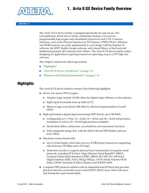
1–4 Chapter 1: <strong>Arria</strong> <strong>II</strong> <strong>GX</strong> Device <strong>Family</strong> <strong>Overview</strong><strong>Arria</strong> <strong>II</strong> <strong>GX</strong> Device Architecture<strong>Arria</strong> <strong>II</strong> <strong>GX</strong> devices are available in up to four speed grades: –3 (fastest), –4, –5, and –6(slowest). Table 1–3 lists the speed grades for <strong>Arria</strong> <strong>II</strong> <strong>GX</strong> devices.Table 1–3. Speed Grades for <strong>Arria</strong> <strong>II</strong> <strong>GX</strong> <strong>Devices</strong>Device358-Pin Flip ChipUBGA<strong>Arria</strong> <strong>II</strong> <strong>GX</strong> Device Architecture572-Pin Flip ChipFBGA780-Pin Flip ChipFBGA<strong>Arria</strong> <strong>II</strong> <strong>GX</strong> devices include a customer-defined feature set optimized forcost-sensitive applications and offer a wide range of density, memory, embeddedmultiplier, I/O, and packaging options. <strong>Arria</strong> <strong>II</strong> <strong>GX</strong> devices support external memoryinterfaces and I/O protocols required by wireless, wireline, broadcast, computer,storage, and military markets. They inherit the 8-input ALM, M9K embedded RAMblock, and high-performance DSP blocks from the Stratix ® IV device family with acost-optimized I/O cell and a transceiver optimized for 6.375 Gbps speeds.Figure 1–1 shows an overview of the <strong>Arria</strong> <strong>II</strong> <strong>GX</strong> device architecture.1152-Pin Flip ChipFBGAEP2A<strong>GX</strong>45 C4, C5, C6, I5 C4, C5, C6, I3, I5 C4, C5, C6, I3, I5 —EP2A<strong>GX</strong>65 C4, C5, C6, I5 C4, C5, C6, I3, I5 C4, C5, C6, I3, I5 —EP2A<strong>GX</strong>95 — C4, C5, C6, I3, I5 C4, C5, C6, I3, I5 C4, C5, C6, I3, I5EP2A<strong>GX</strong>125 — C4, C5, C6, I3, I5 C4, C5, C6, I3, I5 C4, C5, C6, I3, I5EP2A<strong>GX</strong>190 — — C4, C5, C6, I3, I5 C4, C5, C6, I3, I5EP2A<strong>GX</strong>260 — — C4, C5, C6, I3, I5 C4, C5, C6, I3, I5Figure 1–1. <strong>Arria</strong> <strong>II</strong> <strong>GX</strong> Device Architecture <strong>Overview</strong>PLLDLLHigh-Speed Differential I/O,General Purpose I/O, andMemory InterfaceHigh-Speed Differential I/O,General Purpose I/O, andMemory InterfacePLLFPGA Fabric(Logic Elements, DSP,Embedded Memory, Clock Networks)High-SpeedDifferential I/Owith DPA,GeneralPurposeI/O, andMemoryInterfaceTransceiverBlocksAll the blocks in this graphic are for the largest density in the<strong>Arria</strong> <strong>II</strong> <strong>GX</strong> family. The number of blocks can vary based onthe density of the device.PLLPLLPlug and Play PCIe hard IP× 1, ×4, and ×8High-SpeedDifferential I/Owith DPA,GeneralPurposeI/O, andMemoryInterfacePLLHigh-Speed Differential I/O,General Purpose I/O, andMemory InterfaceHigh-Speed Differential I/O,General Purpose I/O, andMemory InterfaceDLLPLL<strong>Arria</strong> <strong>II</strong> <strong>GX</strong> Device Handbook, Volume 1 © July 2010 Altera Corporation
Chapter 1: <strong>Arria</strong> <strong>II</strong> <strong>GX</strong> Device <strong>Family</strong> <strong>Overview</strong> 1–5<strong>Arria</strong> <strong>II</strong> <strong>GX</strong> Device ArchitectureHigh-Speed Transceiver Features<strong>Arria</strong> <strong>II</strong> <strong>GX</strong> devices integrate up to 16 transceivers on a single device. The transceiverblock is optimized for cost and power consumption. <strong>Arria</strong> <strong>II</strong> <strong>GX</strong> transceivers supportthe following features:■■■■Configurable pre-emphasis and equalization, and adjustable output differentialvoltageFlexible and easy-to-configure transceiver datapath to implement proprietaryprotocolsSignal integrity features■■■■Programmable transmitter pre-emphasis to compensate for inter-symbolinterference (ISI)User-controlled five-stage receiver equalization with up to 7 dB ofhigh-frequency gainOn-die power supply regulators for transmitter and receiver PLL charge pumpand voltage-controlled oscillator (VCO) for superior noise immunityCalibration circuitry for transmitter and receiver on-chip termination (OCT)resistorsDiagnostic features■■■■■Serial loopback from the transmitter serializer to the receiver CDR fortransceiver physical coding sublayer (PCS) and physical media attachment(PMA) diagnosticsParallel loopback from the transmitter PCS to the receiver PCS with built-in selftest (BIST) pattern generator and verifierReverse serial loopback pre- and post-CDR to transmitter buffer for physicallink diagnosticsLoopback master and slave capability in PCIe hard IP blocksSupport for protocol features such as MSB-to-LSB transmission in aSONET/SDH configuration and spread-spectrum clocking in a PCIeconfiguration© July 2010 Altera Corporation <strong>Arria</strong> <strong>II</strong> <strong>GX</strong> Device Handbook, Volume 1
Chapter 1: <strong>Arria</strong> <strong>II</strong> <strong>GX</strong> Device <strong>Family</strong> <strong>Overview</strong> 1–7<strong>Arria</strong> <strong>II</strong> <strong>GX</strong> Device ArchitecturePCIe Hard IP BlockEvery <strong>Arria</strong> <strong>II</strong> <strong>GX</strong> device includes an integrated hard-IP block which implementsPCIe PHY/MAC, data link, and transaction layers. This PCIe hard IP block is highlyconfigurable to meet the requirements of the majority of PCIe applications. PCIe hardIP makes implementing a PCIe Gen1 solution in your <strong>Arria</strong> <strong>II</strong> <strong>GX</strong> design simple andeasy.You can instantiate PCIe hard IP block using the PCI Compiler MegaWizard TM Plug-InManager, similar to soft IP functions, but does not consume core FPGA resources orrequire placement, routing, and timing analysis to ensure correct operation of thecore. The <strong>Arria</strong> <strong>II</strong> <strong>GX</strong> PCIe hard IP block includes support for:■■■■×1, ×4, and ×8 lane configurationsRoot port and endpoint configurations512-byte payloadCompliant to PCIe 1.1 at 2.5 GbpsLogic Array Block and Adaptive Logic ModulesEmbedded Memory Blocks■■■■■■■Logic array blocks (LABs) consists of 10 ALMs, carry chains, shared arithmeticchains, LAB control signals, local interconnect, and register chain connection linesALMs expand the traditional four-input LUT architecture to eight-inputs,increasing performance by reducing logic elements (LEs), logic levels, andassociated routingLABs have a derivative called MLAB, which adds SRAM-memory capability tothe LABMLAB and LAB blocks always coexist as pairs, allowing up to 50% of the logic(LABs) to be traded for memory (MLABs)M9K embedded memory blocks provide up to 8,550 Kbits of on-chip memorycapable of up to 390-MHz performance. The embedded memory structure consistsof columns of M9K memory blocks that you can configure as RAM, FIFO buffers,and ROM.Optimized for applications such as high-throughput packet processing,high-definition (HD) line buffers for video processing functions, and embeddedprocessor program and data storage.The Quartus ® <strong>II</strong> software allows you to take advantage of M9K memory blocks byinstantiating memory using a dedicated megafunction wizard or by inferringmemory directly from VHDL or Verilog source code.© July 2010 Altera Corporation <strong>Arria</strong> <strong>II</strong> <strong>GX</strong> Device Handbook, Volume 1
1–8 Chapter 1: <strong>Arria</strong> <strong>II</strong> <strong>GX</strong> Device <strong>Family</strong> <strong>Overview</strong><strong>Arria</strong> <strong>II</strong> <strong>GX</strong> Device ArchitectureTable 1–5 lists the <strong>Arria</strong> <strong>II</strong> <strong>GX</strong> device memory modes.Table 1–5. Memory Modes for <strong>Arria</strong> <strong>II</strong> <strong>GX</strong> <strong>Devices</strong>Port ModePort Width ConfigurationSingle Port ×1, ×2, ×4, ×8, ×9, ×16, ×18, ×32, and ×36Simple Dual Port ×1, ×2, ×4, ×8, ×9, ×16, ×18, ×32, and ×36True Dual Port ×1, ×2, ×4, ×8, ×9, ×16, and ×18DSP ResourcesI/O Features■■■■■■Fulfills the DSP requirements of 3G and Long Term Evolution (LTE) wirelessinfrastructure applications, video processing applications, and voice processingapplicationsDSP block input registers efficiently implement shift registers for finite impulseresponse (FIR) filter applicationsThe Quartus <strong>II</strong> software includes megafunctions you can use to control the modeof operation of the DSP blocks based on user-parameter settingsYou can directly infer multipliers from the VHDL or Verilog HDL source codeContains up to 12 modular I/O banksAll I/O banks support a wide range of single-ended and differential I/Ostandards, as listed in Table 1–6Table 1–6. I/O Standards Support for <strong>Arria</strong> <strong>II</strong> <strong>GX</strong> <strong>Devices</strong>TypeSingle-Ended I/ODifferential I/OI/O StandardLVTTL, LVCMOS, SSTL, HSTL, PCIe, and PCI-XSSTL, HSTL, LVPECL, LVDS, mini-LVDS, Bus LVDS (BLVDS), and RSDS■■■■Supports programmable bus hold, programmable weak pull-up resistors, andprogrammable slew rate controlCalibrates OCT or driver impedance matching for single-ended I/O standardswith one OCT calibration block on the top-left, top-right, and bottom-left cornersof the deviceDedicated configuration banks at Bank 3C and 8C which support dedicatedconfiguration pins and some of the dual-purpose pins with a configurationscheme at 1.8, 2.5, 3.0, and 3.3 VDedicated VREF pin per I/O bank to allow voltage-referenced I/O standards. EachI/O bank can operate at independent V CCIO and V REF levels<strong>Arria</strong> <strong>II</strong> <strong>GX</strong> Device Handbook, Volume 1 © July 2010 Altera Corporation
Chapter 1: <strong>Arria</strong> <strong>II</strong> <strong>GX</strong> Device <strong>Family</strong> <strong>Overview</strong> 1–9<strong>Arria</strong> <strong>II</strong> <strong>GX</strong> Device ArchitectureHigh-Speed LVDS I/O and DPA■■■■Clock Management■■■Dedicated circuitry for implementing LVDS interfaces at speeds from 150 Mbps to1.25 GbpsR D OCT for high-speed LVDS interfacingDPA circuitry and soft-CDR circuitry at the receiver automatically compensates forchannel-to-channel and channel-to-clock skew in source-synchronous interfacesand allows for implementation of asynchronous serial interfaces with embeddedclocks at data rates from 150 Mbps to 1.25 GbpsEmulated LVDS output buffers use two single-ended output buffers with anexternal resistor network to support LVDS, mini-LVDS, BLVDS, and RSDSstandards.Provides dedicated global clock networks (GCLKs), regional clock networks(RCLKs), and periphery clock networks (PCLKs) that are organized into ahierarchical structure that provides up to 148 unique clock domainsUp to six PLLs with seven outputs per PLL to provide robust clock managementand synthesis■■■Independently programmable PLL outputs, creating a unique andcustomizable clock frequency with no fixed relation to any other clockInherent jitter filtration and fine granularity control over multiply and divideratiosSupports spread-spectrum input clocking and counter cascading with PLLinput clock frequencies ranging from 5 to 500 MHz to support both low-costand high-end clock performanceFPGA fabric can use the unused transceiver PLLs to provide more flexibilityAuto-Calibrating External Memory Interfaces■■■I/O structure enhanced to provide flexible and cost-effective support for differenttypes of memory interfacesContains features such as OCT and DQ/DQS pin groupings to enable rapid androbust implementation of different memory standardsAn auto-calibrating megafunction is available in the Quartus <strong>II</strong> software forDDR SDRAM, DDR2 SDRAM, and DDR3 SDRAM memory interface PHYs; themegafunction takes advantage of the PLL dynamic reconfiguration feature tocalibrate based on the changes of process, voltage, and temperature (PVT).© July 2010 Altera Corporation <strong>Arria</strong> <strong>II</strong> <strong>GX</strong> Device Handbook, Volume 1
1–10 Chapter 1: <strong>Arria</strong> <strong>II</strong> <strong>GX</strong> Device <strong>Family</strong> <strong>Overview</strong><strong>Arria</strong> <strong>II</strong> <strong>GX</strong> Device ArchitectureTable 1–7 lists the preliminary external memory support.Table 1–7. External Memory Interface Maximum Performance for <strong>Arria</strong> <strong>II</strong> <strong>GX</strong> <strong>Devices</strong>—PreliminaryMemory TypeDDR SDRAMDDR2 SDRAMDDR3 SDRAMQDR <strong>II</strong>+/QDR <strong>II</strong> SRAMMaximum Performance200 MHz333 MHz400 MHz250 MHzfFor more information about the external memory interfaces support, refer to theExternal Memory Interfaces in <strong>Arria</strong> <strong>II</strong> <strong>GX</strong> <strong>Devices</strong> chapter.Nios <strong>II</strong>■■<strong>Arria</strong> <strong>II</strong> <strong>GX</strong> devices support all variants of the NIOS ® <strong>II</strong> processorNios <strong>II</strong> processors are supported by an array of software tools from Altera andleading embedded partners and are used by more designers than any otherconfigurable processorConfiguration Features■■■Configuration■Supports active serial (AS), passive serial (PS), fast passive parallel (FPP), andJTAG configuration schemes.Design Security■■Supports programming file encryption using 256-bit volatile and non-volatilesecurity keys to protect designs from copying, reverse engineering, andtampering in FPP configuration mode with an external host (such as a MAX ® <strong>II</strong>device or microprocessor), or when using the AS or PS configuration schemeDecrypts an encrypted configuration bitstream using the AES algorithm, anindustry standard encryption algorithm that is FIPS-197 certified and requiresa 256-bit security keyRemote System Upgrade■■■Allows error-free deployment of system upgrades from a remote locationsecurely and reliably without an external controllerSoft logic (either the Nios <strong>II</strong> embedded processor or user logic) implementationin the device helps download a new configuration image from a remotelocation, store it in configuration memory, and direct the dedicated remotesystem upgrade circuitry to start a reconfiguration cycleDedicated circuitry in the remote system upgrade helps to avoid system downtime by performing error detection during and after the configuration process,recover from an error condition by reverting back to a safe configurationimage, and provides error status information<strong>Arria</strong> <strong>II</strong> <strong>GX</strong> Device Handbook, Volume 1 © July 2010 Altera Corporation
Chapter 1: <strong>Arria</strong> <strong>II</strong> <strong>GX</strong> Device <strong>Family</strong> <strong>Overview</strong> 1–11Reference and Ordering InformationSEU Mitigation■■■Offers built-in error detection circuitry to detect data corruption due to soft errorsin the configuration random access memory (CRAM) cellsAllows all CRAM contents to be read and verified to match aconfiguration-computed cyclic redundancy check (CRC) valueYou can identify and read out the bit location and the type of soft error through theJTAG or the core interfaceJTAG Boundary Scan Testing■■■Supports JTAG IEEE Std. 1149.1 and IEEE Std. 1149.6 specificationsIEEE Std. 1149.6 supports high-speed serial interface (HSSI) transceivers andperforms boundary scan on alternating current (AC)-coupled transceiver channelsBoundary-scan test (BST) architecture offers the capability to test pin connectionswithout using physical test probes and capture functional data while a device isoperating normallyReference and Ordering InformationFigure 1–2 describes the ordering codes for <strong>Arria</strong> <strong>II</strong> <strong>GX</strong> devices.Figure 1–2. Packaging Ordering Information <strong>Arria</strong> <strong>II</strong> <strong>GX</strong> <strong>Devices</strong>EP2A<strong>GX</strong> 45 C F 17 C4N<strong>Family</strong> S i g n a t u r eEP2A<strong>GX</strong>Device Density45, 65, 95125, 190, 260Transceiver CountC: 4D: 8E: 12F:16Optional SuffixIndicates specific device shipment methodES: Engineering sampleN: Lead-free devicesSpeed Grade3, 4, 5, or 6, with 3 being the fastestOperating TemperatureC: Commercial temperature (tJ = 0°C to 85°C)I: Industrial temperature (tJ = -40°C to 100°C)Package TypeF: FineLine BGA (FBGA)U: Micro BGA (UFBGA)Ball Array DimensionCorresponds to pin count17 = 358 pins25 = 572 pins29 = 780 pins35 = 1152 pins© July 2010 Altera Corporation <strong>Arria</strong> <strong>II</strong> <strong>GX</strong> Device Handbook, Volume 1
1–12 Chapter 1: <strong>Arria</strong> <strong>II</strong> <strong>GX</strong> Device <strong>Family</strong> <strong>Overview</strong>Document Revision HistoryDocument Revision HistoryTable 1–8 lists the revision history for this chapter.Table 1–8. Document Revision HistoryDate Version Changes MadeJuly 2010 3.0 Updated for the Quartus <strong>II</strong> software version 10.0 release:■Added information about –I3 speed grade■ Updated Table 1–1, Table 1–3, and Table 1–7■ Updated Figure 1–2■■Updated “Highlights” and “High-Speed LVDS I/O and DPA”sectionMinor text editsNovember 2009 2.0 ■ Updated Table 1–1, Table 1–2, and Table 1–3June 2009 1.1 ■ Updated Table 1–2.February 2009 1.0 Initial release.■■Updated “Configuration Features” sectionUpdated “I/O Features” section.<strong>Arria</strong> <strong>II</strong> <strong>GX</strong> Device Handbook, Volume 1 © July 2010 Altera Corporation