Medical Applications Guide (Rev. B - Mouser Electronics
Medical Applications Guide (Rev. B - Mouser Electronics
Medical Applications Guide (Rev. B - Mouser Electronics

You also want an ePaper? Increase the reach of your titles
YUMPU automatically turns print PDFs into web optimized ePapers that Google loves.
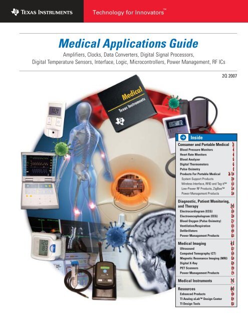
TMTechnology for Innovators<strong>Medical</strong> <strong>Applications</strong> <strong>Guide</strong>Amplifiers, Clocks, Data Converters, Digital Signal Processors,Digital Temperature Sensors, Interface, Logic, Microcontrollers, Power Management, RF ICs2Q 2007➔InsideConsumer and Portable <strong>Medical</strong> 3Blood Pressure Monitors 4Heart Rate Monitors 4Blood Analyzer 5Digital Thermometers 6Pulse Oximetry 7Products For Portable <strong>Medical</strong> 8-16System Support Products 10Wireless Interface, RFID and Tag-it 12Low-Power RF Products, ZigBee 14Power Management Products 16Diagnostic, Patient Monitoring,and Therapy 20Electrocardiogram (ECG) 20Electroencephalogram (EEG) 20Blood Oxygen (Pulse Oximetry) 27Ventilation/Respiration 33Defibrillators 40Power Management Products 43<strong>Medical</strong> Imaging 47Ultrasound 47Computed Tomography (CT) 55Magnetic Resonance Imaging (MRI) 59Digital X-Ray 65PET Scanners 70Power Management Products 74<strong>Medical</strong> Instruments 76Resources 80Enhanced Products 80TI Analog eLab Design Center 81TI Design Tools 82
2➔<strong>Medical</strong> <strong>Applications</strong> <strong>Guide</strong>Table of ContentsConsumer and Portable <strong>Medical</strong>Blood Pressure Monitors . . . . . . . . . . . . . . . . . . . . . . . . . . . . . . . . . . . . . . . .4Heart Rate Monitors . . . . . . . . . . . . . . . . . . . . . . . . . . . . . . . . . . . . . . . . . . . .4Blood Analyzer . . . . . . . . . . . . . . . . . . . . . . . . . . . . . . . . . . . . . . . . . . . . . . . .5Digital Thermometers . . . . . . . . . . . . . . . . . . . . . . . . . . . . . . . . . . . . . . . . . . .6Pulse Oximetry . . . . . . . . . . . . . . . . . . . . . . . . . . . . . . . . . . . . . . . . . . . . . . . .7Products for Portable <strong>Medical</strong> . . . . . . . . . . . . . . . . . . . . . . . . . . . . . . . . . .8-16System Support Products . . . . . . . . . . . . . . . . . . . . . . . . . . . . . . . . . . . . .10Wireless Interface, RFID and Tag-it . . . . . . . . . . . . . . . . . . . . . . . . . . . .12Low-Power RF Products, ZigBee . . . . . . . . . . . . . . . . . . . . . . . . . . . . . .14Power Management Products for Portable <strong>Applications</strong> . . . . . . . . . . . . .16Diagnostic, Patient Monitoring and TherapyElectrocardiogram (ECG) . . . . . . . . . . . . . . . . . . . . . . . . . . . . . . . . . . . . . . . .20Electroencephalogram (EEG) . . . . . . . . . . . . . . . . . . . . . . . . . . . . . . . . . . . . .20Blood Oxygen (Pulse Oximetry) . . . . . . . . . . . . . . . . . . . . . . . . . . . . . . . . . . .27Ventilation/Respiration . . . . . . . . . . . . . . . . . . . . . . . . . . . . . . . . . . . . . . . . .33Defibrillators . . . . . . . . . . . . . . . . . . . . . . . . . . . . . . . . . . . . . . . . . . . . . . . . .40Power Management Products for Diagnostic <strong>Applications</strong> . . . . . . . . . . . . .43IMPORTANT NOTICE: TI products are not authorized for use insafety-critical applications (such as FDA Class 3 applications)where a failure of the TI product would reasonably be expectedto cause severe personal injury or death, unless officers of theparties have executed an agreement specifically governing suchuse. Systems and equipment manufacturers and designers whoincorporate TI products into their end products represent thatthey have all necessary expertise in the safety and regulatoryramifications of its application, and they acknowledge and agreethat they are solely responsible for all legal, regulatory andsafety-related requirements concerning their products and anyuse of TI products in such safety-critical applications, notwithstandingany applications-related information or support thatmay be provided by TI. Further, systems and equipment manufacturersand designers who incorporate TI products into their endproducts agree to fully indemnify TI and its representativesagainst any damages arising out of the use of TI products in suchsafety-critical applications.<strong>Medical</strong> ImagingUltrasound . . . . . . . . . . . . . . . . . . . . . . . . . . . . . . . . . . . . . . . . . . . . . . . . . . .47Computed Tomography (CT) . . . . . . . . . . . . . . . . . . . . . . . . . . . . . . . . . . . . .55Magnetic Resonance Imaging (MRI) . . . . . . . . . . . . . . . . . . . . . . . . . . . . . .58Digital X-Ray . . . . . . . . . . . . . . . . . . . . . . . . . . . . . . . . . . . . . . . . . . . . . . . . .65PET Scanners . . . . . . . . . . . . . . . . . . . . . . . . . . . . . . . . . . . . . . . . . . . . . . . .70Power Management Products for Imaging <strong>Applications</strong> . . . . . . . . . . . . . . .74<strong>Medical</strong> Instruments<strong>Medical</strong> Instrumentation . . . . . . . . . . . . . . . . . . . . . . . . . . . . . . . . . . . . . . .76ResourcesEnhanced Products . . . . . . . . . . . . . . . . . . . . . . . . . . . . . . . . . . . . . . . . . . . .80TI Analog eLab Design Center . . . . . . . . . . . . . . . . . . . . . . . . . . . . . . . . . .81TI Design Tools . . . . . . . . . . . . . . . . . . . . . . . . . . . . . . . . . . . . . . . . . . . . . . .82<strong>Medical</strong> <strong>Applications</strong> <strong>Guide</strong> Texas Instruments 2Q 2007
Consumer and Portable <strong>Medical</strong> Devices3Consumer and Portable <strong>Medical</strong> <strong>Applications</strong> Discussion➔➔In This SectionPortable <strong>Medical</strong> <strong>Applications</strong> 3Blood Pressure and Heart Rate Monitors 4Blood Analyzer 5Digital Thermometers 6Pulse Oximetry 7System Support Products 10Wireless Interface, RFID and Tag-it 12Low-Power RF Products 14Low-Power RF Products, ZigBee 15Power Management for Portable Devices 16Products for Portable <strong>Medical</strong> 18Portable <strong>Medical</strong> <strong>Applications</strong>Whether developing a blood glucose meter, digital blood pressuremeter, blood gas meter, digital pulse/heart rate monitor or even adigital thermometer, there are five system level blocks that arecommon to each one: Power/Battery Management, Control andData Processing, Amplification and A/D Conversion of the sensorinput, some type of display and the sensor element(s) itself. In general,these are all battery-operated, microcontroller-controlled handhelddevices that take measurements using various bio-sensors. Obviously,the actual implementation topology of these blocks will differ greatlywith the sensing, processing and information display demands ofthe meter type and feature set.Key design considerations are ultra-low power consumption andhigh efficiency driven by the need for extended battery life, and highprecision with a fast response time driven by the user’s need to quicklyknow their health status. Additional requirements may drive needs foradditional memory to allow for historical profiling, cabled or wirelessinterfaces for data upload to a computer at home or in the doctor’soffice or even for access to the sensor, and possibly audio feedbackfor simple good/not good indication or more complex step-by-steputilization instructions. Adding these features without increasingpower consumption is a significant challenge. Texas Instruments offersa broad portfolio of high-performance Microcontrollers, Digital SignalProcessors (DSPs), Instrumentation, Operational and Buffer Amplifiers,Data Converters, Power and Battery Management, Audio Amplifiers,and both Wired and Wireless Interface components.Bio-SensorPrecisionReferenceInstrumentationAmpBufferAmpMSP430LCDDisplayOP AMPCore Portable <strong>Medical</strong> System(Processor, Memory, Display, Keypad,Power, Battery Management)LCD ControllerFlashADCLCDBacklightMSP430µControllerSystem Based and OperationalFunctional Blocks inPortable <strong>Medical</strong> SystemsUSBControllerZigBeeBluetooth ®Low Power WirelessTransientProtectionWireless DataTransmission orSensor AccessWired DataTransmissionAFE PowerClockKeypadLEDDriverCurrent Limit SwitchCard Slotfor SystemCalibrationµControllerandMemory PowerFuelGaugeLithiumBatteryProtectionBattery ManagementBatteryChargerAudioFeedback orInstructionsOptionalACAdapterPlugAC LineGeneral block diagram for typical portable medical devices.Texas Instruments 2Q 2007www.ti.com/medical<strong>Medical</strong> <strong>Applications</strong> <strong>Guide</strong>
4➔Consumer and Portable <strong>Medical</strong> DevicesBlood Pressure and Heart Rate MonitorsBlood Pressure MonitorThe system uses either Korotkoff, Oscillometry, or Pulse Transit Timemethods to measure blood pressure. It employs a pressure cuff andpump, plus a transducer to measure blood pressure and heart rate inthree phases: Inflation, Measurement, and Deflation. It includes anLCD, selection buttons, memory recall, power management and USBinterface.The core subsystems include:Processor/Memory — The digital pressure measurement and heartrate are performed by the microprocessor. Measurement results arestored in Flash memory as a data log that can be uploaded to a PCvia USB.User Interface — Allows the user to control the pressuremeasurement process and read the results on a LCD display.Sensor Interface — Allows the processor to control the cuffinflation/deflation and sense blood pressure which is amplifiedby instrumentation amplifiers and digitized by the ADC.Power Conversion — Converts input power from the alkaline batteryto run various functional blocks.PressureSensorPowerManagementEEPROMKeypadAmplifierMicrocontrollerDigital I/OsMemory(Flash)LCD Control(LCD Driver,SPI, or I 2 C)12- to 16-BitADCReferenceAudio Output(PWM/DAC)RTCMotorControlExample application block diagram – blood pressure monitor.LCDDisplaySpeech/SoundDCMotorInterfaceto PC(RS232, USB,Wireless)Heart Rate MonitorThe heart generates an electrochemicalimpulse that spreads out inthe heart in such a fashion as to causethe cells to contract and relax in atimely order and thus give the heart apumping characteristic. This sequenceis initiated by a group of nerve cellscalled the sinoatrial (SA) node resultingin a polarization and depolarizationof the cells of the heart. Because thisaction is electrical in nature andbecause the body is conductive withits fluid content, this electrochemicalaction can be measured at the surfaceof the body.Input SignalsHeartSignalSkinTemperatureNTCThermistorOPA2333AmplifierAmplifierMSP430F1222BandpassFilterDigitalSignalProcessingDisplayThe graphics illustrates a multifunction system to measure heart rate and skin temperature using OPA2333and MSP430.User Input➔Note:“Heart Rate and EKG Monitor using the MSP430FG439” (slaa280)www-s.ti.com/sc/techlit/slaa280<strong>Medical</strong> <strong>Applications</strong> <strong>Guide</strong> Texas Instruments 2Q 2007
6➔Consumer and Portable <strong>Medical</strong> DevicesDigital ThermometersDigital ThermometersDigital thermometers are quickly replacing traditional mercury thermometers.Digital thermometers are fast, accurate and effective. Withnewer technologies, different types of digital fever thermometers maybe classified on the basis of the location where they are used such asoral, rectal, underarm, ear, etc. The ear thermometer measures theinfrared heat of the eardrum, which reflects the temperature of thehypothalamus — the temperature-controlling system of the brain.Infrared sensors are used in ear thermometers for measurement,while thermopiles or thermistors may be used in other types.Depending on cost considerations, different types of digital thermometersare available. High-end thermometers have a number ofthermopiles or thermistors, whose resistance changes with temperature.The change in resistance is measured as a change in voltage. Thisanalog voltage is converted digitally by an analog-to-digital converter(ADC). The speed and resolution of this ADC depends on the accuracyand time at which information is needed. However, if an ADC moduleis not available, then it is possible to digitize the analog signal by usinga comparator and a timer, using slope A/D conversion. This method isgenerally used in low-cost versions of digital thermometers. The singleslope conversion is a simple method for measuring temperature.Capacitance, supply voltage and frequency changes caused by agingor temperature drift can be compensated by using a ratio metricmeasurement principle. Detailed information about the slope conversionprinciple can be found in the application note “Implementing anUltra-Low-Power Thermostat with Slope A/D Conversion” (SLAA129).The block diagrams at right show both the low-end general-purposeand high-end versions of digital thermometers. Typical ADC resolutionused in general-purpose digital thermometers may be 12-bit and abovedepending on the accuracy level required. A good reference for theADC is also required for better accuracy. A microcontroller may beused for control purposes. Low-cost solutions employ a low-cost,low-power microcontroller like the MSP430, which has the integratedcomparator and timer to digitize the analog signal using the slopeA/D conversion technique.Other additional features like high temperature alarm, beep aftermeasurement, auto shut-off and data log of previous temperaturesmay also be featured in thermometers. Most thermometers haveeasy-to-read displays, usually a LCD display and low-battery indicator.Other peripherals include digital I/Os and LCD drivers.TThermopileor ThermistorOp AmpMSP430 MicrocontrollerDigital I/OsComparatorTimerMSP430 MicrocontrollerADC(>12 Bits)ReferenceLCD Control(LCD Driveror I 2 C)Digital I/OsA general block diagram of a low-cost digital thermometer.LCD Control(LCD Driveror I 2 C)MemoryDigital I/OsMemoryKeypadA general block diagram of a digital thermometer with high accuracy.LCDKeypadLCD<strong>Medical</strong> <strong>Applications</strong> <strong>Guide</strong> Texas Instruments 2Q 2007
8➔Consumer and Portable <strong>Medical</strong> DevicesPortable <strong>Medical</strong>MSP430FG461x Offers Complete System-on-Chipfor High-Precision, Portable InstrumentationMSP430FG4616, MSP430FG4617, MSP430FG4618,MSP430FG4619Get samples, datasheets, evaluation modules and app reports at:www.ti.com/sc/device/PARTnumber(Replace PARTnumber with MSP430FG4616, MSP430FG4617,MSP430FG4618 or MSP430FG4619)The MSP430FG461x microcontroller (MCU) series is designed forhigh-precision, real-time portable applications that require highlyintegrated intelligent peripherals and larger memory options on asingle chip. The MCU’s extended 1MB memory model enables fastercode execution that results in up to 50% reduction in cycles for a fullcontext store and up to 25% when addressing peripherals, Flash orRAM. The MCU configurations are complete with two 16-bit timers,a high-performance 12-bit A/D converter, dual 12-bit D/A converters,three configurable operational amplifiers, one universal serialcommunication interface (USCI), one universal synchronous/asynchronous communication interface (USART), DMA, 80 I/O pinsand a liquid crystal display (LCD) driver with regulated charge pump.Key Features• Up to 120kB Flash/8kB RAM• Ultra-low-power RTC operation• Zero-power brown-out reset• Complete system-on-chip:• UART, SPI, I 2 C, IrDA• OPA-ADC-MDA-DAC-OPA• Voltage-programmable LCD driver• Trace buffer on chip• Easy to use<strong>Applications</strong>• High-precision, battery-powered applications such as:• Portable medical• Portable industrial• Low-power RFXIN/ XIN/XT21n XT21nDVCC1/2DVSS1/2 AVCC AVSS P1.x/P2.x2x8P3.x/P4.xP5.x/P6.x4x8P7.x/P8.xP9.x/P10.x4x8/2x16OscillatorsFLL+MCLKCopySMCLKFlash (FG)ROM (CG)120kB116kB93kB92kBRAM4kB8kB8kB4kBADC1212-Bit12ChannelsDAC1212-Bit2 ChannelsVoltage OutOA0, OA1,OA23 Op AmpsComparator_APorts P1/P22x8 I/OInterruptCapabilityPortsP3/P4P5/P64x8 I/OPortsP7/P8P9/P104x8 / 2x16I/O8MHzCPUXIncl. 16RegistersMABMDBDMAController3 ChannelsEnahncedEmulation(FG Only)JTAGInterfaceBrownoutProtectionSVS/SVMHardwareMultiplierMPY,MPYS,MAC,MACSWatchdogWDT+15/16-BitTimer_A33CCRegistersTimer_B77CCRegistersShadowRegBasic TimerandReal-TimeClockLCD_A160Segments1, 2, 3, 4MuxUSCI_A0:UART,IrDA, SPIUSCI_B0:SPI, I 2 CUSART1UART, SPIRST/NMIMPS430FG461x functional block diagram.<strong>Medical</strong> <strong>Applications</strong> <strong>Guide</strong> Texas Instruments 2Q 2007
Consumer and Portable <strong>Medical</strong> DevicesPortable <strong>Medical</strong>9➔15ppm/°C (max), 100µA, SOT23-3 SeriesVoltage ReferencesREF3112, REF3120, REF3125, REF3130, REF3133,REF3140Get samples, datasheets, evaluation modules and app reports at:www.ti.com/sc/device/PARTnumber(Replace PARTnumber with REF3112, REF3120, REF3125, REF3130,REF3133 or REF3140)The REF31xx is a family of precision, low-power, low-dropout seriesvoltage references. The REF31xx does not require a load capacitor, butis stable with any capacitive load and can sink/source up to 10mA ofoutput current. Unloaded, the REF31xx can be operated on suppliesdown to 5mV above the output voltage.ProductVoltage (V)REF3112 1.25REF3120 2.048REF3125 2.5REF3130 3.0REF3133 3.3REF3140 4.096Key Features• Low dropout: 5mV• High output current: ±10mA• High accuracy: 0.2% (max)• Low I Q : 115µA (max)• Excellent specified drift performance:• 15ppm/°C (max) from 0°C to +70°C• 20ppm/°C (max) from –40°C to +125°C<strong>Applications</strong>• <strong>Medical</strong> equipment• Data acquisition systems• Portable, battery-powered equipment• Handheld test equipment2.5VREF3112V INV OUT = 1.25VGND0.1µF0V to1.25VBasic data acquisition system.V REF+In–InADS8324GNDV CCCSD OUTDCLOCK5Ω1µF to 10µF2.5V SupplyV S1µF to 10µFMicrocontroller1.8V, microPower CMOS Operational AmplifierZerø-Drift SeriesOPA333, OPA2333Get samples, datasheets, evaluation modules and app reports at:www.ti.com/sc/device/OPA333 or www.ti.com/sc/device/OPA2333The OPA333 series of CMOS operational amplifiers uses a proprietaryauto-calibration technique to simultaneously provide very low offsetvoltage (10µV max) and near-zero drift over time and temperature.These miniature, high-precision, low quiescent current amplifiers offerhigh-impedance inputs that have a common-mode range 100mVbeyond the rails and rail-to-rail output that swings within 50mV ofthe rails. Single or dual supplies as low as +1.8V (±0.9V) and up to+5.5V (±2.75V) may be used. The OPA333 family offers excellentCMRR without the crossover associated with traditional complementaryinput stages. This design results in superior performance fordriving analog-to-digital converters (ADCs) without degradation ofdifferential linearity.Key Features• Low offset voltage: 10µV (max)• Zero drift: 0.05µV/°C (max)• 0.01Hz to 10Hz noise: 1.1µV PP• Quiescent current: 17µA• Supply voltage: 1.8V to 5.5V• Rail-to-rail input/output• Packaging: SC70, SOT23<strong>Applications</strong>• <strong>Medical</strong> instrumentation• Temperature measurements• Battery-powered instruments• Electronic scales• Handheld equipment+5V0.1mF+- -+ +K- TypeThermocouple40.7mV/°CD1REF3140R 46.04kΩ4.096VR 16.04kΩR 22.94kΩR 6200ΩR 360.4ΩOPA333 in temperature measurement circuit.R 531.6kΩR 2549ΩZero Adj.R 9150kΩ+5VOPA3330.1mF+V OTexas Instruments 2Q 2007<strong>Medical</strong> <strong>Applications</strong> <strong>Guide</strong>
10➔Consumer and Portable <strong>Medical</strong> DevicesSystem Support ProductsVoltage Level TranslationAs operating voltage levels in microcontrollers continue to drop, avoid may be created between peripheral devices and processorsthat disrupts interfacing between the devices. TI’s translators enablecommunication between incompatible I/Os with level translationbetween the 1.2V, 1.5V, 1.8V, 2.5V and 3V nodes. The MSP430microcontroller shown in many applications within this guide, hasa 3.6V (max) I/O tolerance: thus, translators can be used to protectthe inputs and to interface to higher voltage peripherals.<strong>Applications</strong>• LCD interface• Interface devices with different supply voltagesSuggested ComponentsV CC Power SmallestRange Max I CC FootprintComponent Description (V) (µA) Pins/PackagesSN74AVC1T45* Single-bit Dual-Supply 1.2 to 3.6 10 6/WCSPBus Transceiver(NanoStar)SN74LVC1T45 Single-bit Dual-Supply 1.65 to 5.5 4 6/WCSPBus Transceiver(NanoStar)SN74AVC2T45* Dual-bit Dual-Supply 1.2 to 3.6 10 8/WCSPTransceiver(NanoStar)SN74LVC2T45 Dual-bit Dual-Supply 1.65 to 5.5 10 8/WCSPTransceiver(NanoStar)SN74AUP1T57 Single-Supply Voltage 2.3 to 3.6 0.9 6/WCSPTranslator(NanoStar)SN74AUP1T58 Single-Supply Voltage 2.3 to 3.6 0.9 6/WCSPTranslator(NanoStar)SN74AUP1T97 Single-Supply Voltage 2.3 to 3.6 0.9 6/WCSPTranslator(NanoStar)SN74AUP1T98 Single-Supply Voltage 2.3 to 3.6 0.9 6/WCSPTranslator(NanoStar)PCA9306 Dual Bidirectional I 2 C-bus — — 8/US, WCSPand SMBus Voltage-LevelTranslator* Bus-hold option available.1.8V CPU1.8VLevelTranslatorV CCADIRA1A2A3A4A5A6A7A8GNDGNDV CCBV CCBOEB1B2B3B4B5B6B7B8GND3.3V3.3VPeripheralI 2 C Bus I/O ExpansionOften there are not enough GPIOs available on the microcontrollerto control all the desired peripherals, such as controlling LEDs orinterfacing to a keypad. An I 2 C bus expander can increase the numberof GPIOs while taking up minimal board space with the 8-pin WCSP.Key Features• Processor pin savings• Improved board routing• Reduced board space<strong>Applications</strong>• Keypad control• LED control• Temperature sensingSuggested ComponentsFrequencyV CC(Max) I 2 C Range -bitComponent (kHz) Address (V) WidthPCA9536 400 1000 001 2.3 to 5.5 4PCF8574 100 0100 xxx 2.5 to 6.0 8PCF8574A 100 0111 xxx 2.5 to 6.0 8PCA9554 400 0011 xxx 2.3 to 5.5 8PCA9557 400 0011 xxx 2.3 to 5.5 8PCA6107 400 0011 xxx 2.3 to 5.5 8PCF8575 400 0100 xxx 2.5 to 5.5 16PCF8575C 400 0100 xxx 4.5 to 5.5 16PCA9535 400 0100 xxx 2.3 to 5.5 16PCA9539 400 1110 1xx 2.3 to 5.5 16PCA9555 400 0100 xxx 2.3 to 5.5 16Pressure Sensor1. Silicon Pressure2. Load Cell3.0VOptionalOp AmpLPV324V REFTLV431B 2.5VPower ManagementCharge PumpSwitching RegulatorExample application block diagram.RS-232I 2C BusMicrocontrollerwith Integrated12-/16-Bit ADCand LCD DriverPower ManagementLDO RegulatorIrDA3.3VKeypadEEPROMLCD DisplayDC MotorExample application block diagram.<strong>Medical</strong> <strong>Applications</strong> <strong>Guide</strong> Texas Instruments 2Q 2007
Consumer and Portable <strong>Medical</strong> DevicesSystem Support Products11➔Audio Signal RoutingOne of the most common applications for analog switches is signalrouting. This may be routing from one source to multiple destinationsor from several sources to a single destination. A single-pole, doublethrowanalog switch can be used for either situation. For example,the switch could be used to reroute the output of the audio poweramplifier to two different speakers. Another common application isswitching from an audio amplifier in the baseband of a mobile toan audio power amplifier for higher power output.<strong>Applications</strong>• DeMUX internal/external speakers• MUX audio power amplifier• Low-power routing (
12➔Consumer and Portable <strong>Medical</strong> DevicesWireless Interface, RFID and Tag-itRadio Frequency Identification (RFID)TI’s high frequency RFID product family consists of 13.56MHz highfrequency(HF) transponders and low-power RFID readers, which arecompliant with the ISO/IEC 15693 and ISO/IEC 18000-3 global openstandards. Typical RFID implementations can include applications suchas asset tracking, access control, blood bag tracking, medical supplytracking, patient/staff authentication, pharmaceutical authentication,medical imaging, product authentication, and remote digital healthcaremanagement – as well as many non-medical related applications.Tag-it HF-I Transponder InlaysTI’s Tag-it HF-I family of transponder inlays consist of 13.56MHzhigh-frequency (HF) transponders that are compliant with the ISO/IEC15693 and ISO/IEC 18000-3 global open standards. These products areavailable in six different antenna shapes with frequency offset forintegration into paper, PVC or other substrates manufactured with TI’spatented laser-tuning process to provide consistent read performance.Prior to delivery, the transponders undergo complete functional andparametric testing in order to provide the high quality customers havecome to expect.Tag-it HF-I Family Product SpecificationsSupported StandardsISO/IEC 15693-2, -3; ISO/IEC18000-3Recommended Operating Frequency13.56MHzFactory Programmed Read Only Numbers64-bitsTypical Programming Cycles (at +25°C) 100,000Data Retention Time (at +55°C)>10 yearsKey Features• ISO/IEC 15693-2, -3; ISO/IEC18000-3• User and factory lock per block• Application Family Identifier (AFI)Standard• 256-bit user memory, 8 x 32-bit• FastSIDPro• 256-bit user memory, 8 x 32-bit• Password-protected write command• Command to disable IC functionality• FastSIDPlus• 2k-bit user memory, 64 x 32 6-bit• Data Storage Format Identifier (DSFID)• Combined inventory read blockTag-it HF-I Plus Inlay ShapesPart Number RI-I11-112A RI-I11-112B RI-I02-112A RI-I02-112B RI-I03-112A RI-I15-112B RI-I16-112A RI-I17-112AAvailable Memory 2k-bits organized in 64 x 32-bit blocksAntenna size (mm) 45 x 45 45 x 45 45 x 76 45 x 76 22.5 x 38 34 x 65 θ 24.2 θ 32.5Foil Pitch (mm) 50.8 + 0.1/ 50.8 + 0.1/ 96 + 0.1/ 96 + 0.1/ 58 +0.1/ 101.6 +0.1/ 50.8 +0.1/ 50.8 +0.1/–0.4 (2 in) –0.4 (2 in) –0.4 (~3.78 in) –0.4 (~3.78 in) –0.4 (~1.89 in) –0.4 (4 in) –0.4 (2 in) –0.4 (2 in)Frequency Offset for Paper PVC Paper PVC Paper/PVC PVC Paper/PVC Paper/PVCLamination MaterialDeliverySingle tape row with 48mm foil width wound on cardboard reelTag-it HF-I Pro Transponder InlaysPart Number RI-I11-114A-S1 RI-I11-114B-S1 RI-I02-114A-S1 RI-I02-114B-S1 RI-I03-114-S1 RI-I16-114-S1 RI-I17-114-S1Available Memory 256-bits organized in 8 x 32-bit blocksFoil Width (mm) 48mm ±0.5mmAntenna size (mm) 45 x 45 45 x 45 45 x 76 45 x 76 22.5 x 38 θ 24.2 θ 32.5Foil Pitch (mm) 50.8 +0.1/–0.4 (2 in) 50.8 +0.1/–0.4 (2 in) 96 +0.1/–0.4 (~3.78 in) 96 +0.1/–0.4 (~3.78 in) 48 +0.1/–0.4 (~1.89 in) 50.8 +0.1/–0.4 (2 in) 50.8 +0.1/–0.4 (2 in)Frequency Offset for Paper PVC Paper PVC Paper/PVC Paper/PVC Paper/PVCLamination MaterialDeliverySingle row tape Wound on cardboard reelTag-it HF-I Standard Transponder InlaysPart Number RI-I11-114A-01 RI-I11-114B-01 RI-I02-114A-01 RI-I02-114B-01 RI-I03-114-01 RI-I16-114-01 RI-I17-114-01Available Memory 256-bits organized in 8 x 32-bit blocksFoil Width (mm) 48mm ±0.5mmAntenna size (mm) 45 x 45 45 x 45 45 x 76 45 x 76 22.5 x 38 θ 24.2 θ 32.5Foil Pitch (mm) 50.8 +0.1/–0.4 (2 in) 50.8 +0.1/–0.4 (2 in) 96 +0.1/–0.4 (~3.78 in) 96 +0.1/–0.4 (~3.78 in) 48 +0.1/–0.4 (~1.89 in) 50.8 +0.1/–0.4 (2 in) 50.8 +0.1/–0.4 (2 in)Frequency Offset for Paper PVC Paper PVC Paper/PVC Paper/PVC Paper/PVCLamination MaterialDeliverySingle row tape wound on cardboard reel<strong>Medical</strong> <strong>Applications</strong> <strong>Guide</strong> Texas Instruments 2Q 2007
Consumer and Portable <strong>Medical</strong> DevicesWireless Interface, RFID and Tag-it13➔Low-Power, Multi-Standard HF RFID ReadersTRF7960,TRF7961Get samples and datasheets at:www.ti.com/sc/device/TRF7960 or www.ti.com/sc/device/TRF7961Complementing the Tag-it HF-I family of transponder inlays, is theTRF7960; a highly integrated analog front end and data framing systemfor any 13.56MHz RFID reader system. Built-in programming optionsmake it useful for a wide range of applications both in proximityand vicinity RFID systems. Its high level of integration, excellentperformance, miniature size and multiple low power modes allowsthe TRF7960 to be used for battery power-constrained medicalapplications.<strong>Applications</strong>• Asset tracking• Access control• Blood bag tracking• <strong>Medical</strong> supply tracking• Patient and staff authentication• Pharmaceutical authentication• <strong>Medical</strong> imaging and data tracking• Product authentication and calibration• Remote digital healthcare management• And many other non-medical related applicationsKey Features• Supports ISO14443A/B, ISO15693 and Tag-it• Completely integrated protocol handling (OSI Model Layer 3 andbelow)• Programmable output power: (100mW or 200mW)• Wide operating voltage range: 2.7V to 5.5 V• Separate, internal high-PSRR LDOs for analog, digital and PAsections provide noise isolation for superior read range and reliability• Parallel 8-bit or Serial 4-pin SPI interface with 12-byte FIFO• Seven, user selectable, ultra-low power modes• Power down:
Consumer and Portable <strong>Medical</strong> DevicesLow-Power RF Products, ZigBee15➔ZigBee for <strong>Medical</strong> <strong>Applications</strong>The world is going wireless and medical applications are no exception.More and more medical devices, especially patient monitoring, canbenefit from wireless ZigBee technology. With the use of wirelesssensors, the patients can move around in the hospital, or even intheir homes, and the sensors will still monitor and send critical healthdata to the hospital or doctor. Being independent of a patient’s exactgeographical location has a positive impact on both the patient andthe hospital.The ZigBee standard enables companies to have a simple, reliable,low-cost and low-power standard-based wireless platform for theirapplication development. TI’s low-power RF portfolio of highperformanceRF ICs offers robust and cost-effectivesolutions for a variety of medical devices.RF-ICs Compliant with IEEE 802.15.4/ZigBeeSpecifications• CC2420: Industry-leading RF transceiver provides maximum flexibilityas it can be combined with microcontroller• CC2430: True System-on-Chip (SoC) with integrated microcontroller• CC2431: SoC with integrated location capabilities• Hardware development kits• High-performance and robust reference designs• Free Z-Stack ZigBee 2006 compliant stack• Free IEEE 802.15.4 MAC softwareZigBee Software Development Suite• Z-Stack: Industry-leading ZigBee protocol stack from TI• Z-Stack: Protocol stack extensions• Z-Tool (debug tool)DigitalAnalogMixedRESET_NXOSC_Q2XOSC_Q1P2_4P2_3P2_2P2_1P2_0P1_7P1_6P1_5P1_4P1_3P1_2P1_1P1_0P0_7P0_6P0_5P0_4P0_3P0_2P0_1P0_0I/O ControllerCC2430RESET32MHzCrystal OSC32.768kHzCrystal OSCDebugInterfaceDMA∆Σ ADCAudio/DC8 ChannelsUSART1USART2Timer 1 (16-Bit)Timer 3 (8-Bit)Timer 4 (8-Bit)WatchdogTimerHigh SpeedRC-OSC3:2kHz RC-OSCClock Mux &Calibration8051 CPUCoreAESEncryptionandDecryptionTimer 2IEEE 802.15.4 MAC TimerCC2430 functional block diagram.On-Chip VoltageRegulatorPower On ResetBrown OutDemodulatorSleep TimerSleep Mode ControllerMemoryArbitratorIRQControlReceiveChainRadio RegistersCSMA/CS StrobeProcessorASC32/64/128kBFlash8kBRAMFlashWriteRadio Data InterfaceRF_PFrequencySynthesizerRF_NV DD (2.0 - 3.6V)DCOUPLModulatorTransmitChaniFIFO and Frame Control<strong>Applications</strong>• Patient monitoring• Hospital equipment trackingFor more information visit: www.ti.com/zigbeeTexas Instruments 2Q 2007<strong>Medical</strong> <strong>Applications</strong> <strong>Guide</strong>
16➔Consumer and Portable <strong>Medical</strong> DevicesPower Management for Portable DevicesHigh PSRR LDOs in Ultra-Small PackagesTPS71710Get samples and datasheets at: www.ti.com/sc/device/TPS71710The TPS717xx family of low-dropout (LDO), low-power linear regulatorsoffer very high power supply rejection (PSRR) while maintaining verylow 50µA ground current in an ultra-small 5-pin SC70 package. Thefamily achieves fast start-up, very low noise, and excellent transientresponse. The TPS717xx is stable with a 1.0µF ceramic outputcapacitor and uses a precision voltage reference and feedbackloop to achieve a worst-case overall accuracy of 3%.Key Features• Input voltage range: 2.5V to 6.5V• Fixed output voltages: 0.9V to 3.3V• Adjustable output voltages: 0.9V to 5.0V• Rated output current: 150mA• Low quiescent current: 50µA• Stable with 1µF ceramic output capacitor• 30µV RMS output noise, 100Hz to 100kHz• 3% accuracy over load/line/temp• Very high PSRR: 70dB at 100Hz, 1kHz• 67dB at 10kHz, 100kHz• 45dB at 1MHz• Package: SC70-5 and 6-pin 2mm x 2mm SON, 1.5mm x 1.5mm SON<strong>Applications</strong>• RF applications• Low noise applications• Camera modules• PLL power supplies• VCO power suppliesI OUT V DO I Q PSRR atComponent (mA) (mV) (µA) 1MHz (dB)TPS717xx 150 170 50 45600mA Switch, Low V IN Boost DC/DC In TSOT-23TPS61070Get samples and datasheets at: www.ti.com/sc/device/TPS61070The TPS6107x is a synchronous DC/DC converter with integratedFETs providing a peak power conversion efficiency of >90% over avery wide load range and a quiescent current of 19µA. 1-cell to 3-cellAlkaline/NiMH and 1-cell Li-Ion battery-powered equipment benefitfrom the 0.9V to 5.5V input voltage range. The 600mA switch currentlimit allows an output current of up to 75mA at 3.3V from a 0.9V input.Key Features• Input voltage range: 0.9V to 5.5V• 75mA at 3.3V V OUT and 0.9V V IN• Switch current limit: 600mA• Up to 90% efficient over wide load range• Quiescent current: 19µA (typ)• Shutdown current: 0.05µA (typ)• Load disconnect during shutdown• Adjustable output voltage up to 5.5V• 1.2MHz switching frequency, synchronous• Package: 3mm x 3mm x 1mm 2 TSOT-23<strong>Applications</strong>• Portable medical devices needing a higher voltage than supplied bybattery• Simple LED backlighting for LCDSmallInductor0.9V to6.5V InputC110µFL14.7 µHSWVBATENVOUTGNDTPS61070FBR1R2C210µFV O3.3V Up to100mASynchronousDesign3 x 3 TSOT-23V IN1µFCeramicINENOUTTPS717xxGND NRV OUT1µFCeramicFunctional block diagram.V IN0.01µF(Optional)Typical application circuit for fixed voltage variations.<strong>Medical</strong> <strong>Applications</strong> <strong>Guide</strong> Texas Instruments 2Q 2007
Consumer and Portable <strong>Medical</strong> DevicesPower Management for Portable Devices17➔Low-Cost, 1-Cell Li-Ion Charger with FET andCurrent Sense in QFN-10bq24081 bqTINYGet samples and datasheets at: www.ti.com/sc/device/bq24081The bq2408x are highly integrated linear Li-Ion charge management ICsoptimized for USB and AC wall adapter charging of single-cell Li-Ionand Li-Polymer batteries. These highly integrated, single-cell Li-Ionbattery charge management ICs can be used for low-dropout chargerdesigns in space-limited, portable applications. They require a minimalset of external components by integrating a 1A charge FET, reverseblockingcircuitry and current sense along with other batterymanagement features.Key Features• Integration: 1A FET, reverse-current protection, current sense,thermal shutdown, 3mm x 3mm 2 QFN-10• Battery management: 4.2V, ±0.5% voltage regulation, chargetermination, safety timer, optional temperature monitoring• Autonomous power-source selection• Battery pre-conditioning with safety timer• bq24080 offers Charge Enable (CE) and Power Good (PG) functions,bq24081 offers Timer Enable (TE) and Temp Sense (TS) functions<strong>Applications</strong>• Any portable medical device powered by 1-cell Li-Ion and chargedfrom a USB portLi-Ion and Li-Pol Battery Gas Gauge IC forPortable <strong>Applications</strong>bq27010Get samples, datasheets, evaluation modules and app reports at:www.ti.com/sc/device/bq27010The bq27010 (bqJUNIOR) series are highly accurate, stand-alone,single-cell, Li-Ion and Li-Pol battery capacity monitoring andreporting components targeted at space-limited, portable applications.Compensation for battery age, temperature, self-discharge anddischarge rate are applied to the capacity measurements to provideavailable time-to empty information across a wide range of operatingconditions. The component can operate directly from a single-cell andcommunicates to the system over a HDQ one-wire (bq27010) or I 2 Cserial interface (bq27210).Key Features• Reports accurate time-to-empty at both measured andhost-requested load values• Automatic capacity reduction with age• Reports temperature, voltage and current• Requires no user calibration• Programmable input/output port• Dynamic end-of-discharge detection delay to allowuse in a high-dynamic load environment<strong>Applications</strong>• Portable medical• Handheld devicesInput PowerFunctional block diagram.bq24081110INOUT92 NCTS3 STAT1TE 874GNDSTAT25V6SSISETR SETTimerEnableLi-Ion or Li-PolBattery PackPack++Pack–TempPACK+HDCR31kΩR7100ΩC30.1µFR8100ΩESQ ProtectionC40.1µF1234BPIV CCCSSD/Cbq27010PCM 10GPIO 9BRP 8BRN5 HDQ BAT 611C30.1µF7PCM TPR410kΩC20.1µFC10.1µFR11kΩR21kΩLi-IonorLi-PdR S0.020PACK–Li-Ion ProtectorFunctional block diagram.Texas Instruments 2Q 2007<strong>Medical</strong> <strong>Applications</strong> <strong>Guide</strong>
18➔Consumer and Portable <strong>Medical</strong> DevicesComponent Recommendations for Portable <strong>Medical</strong> <strong>Applications</strong>Component RecommendationsComponent Description Key Features Benefits Other TI SolutionsAmplifiersINA122 Instrumentation Amp ±50µV (max) input offset, 83dB CMRR, 0.06mA (typ) I QINA126 Instrumentation Amp ±250µV (max) input offset, 83dB CMRR, 0.175mA (typ) I QINA321 Instrumentation Amp ±500µV (max) input offset, 90dB CMRR, 0.04mA (typ) I QINA331 Instrumentation Amp ±500µV (max) input offset, 90dB CMRR, 0.415mA (typ) I QOPA333 Precision Op Amp 1.8V (min) V S , 0.017mA (max)/ch I QOPA364 CMOS Amplifier 1.8V, 7MHz, 90dB CMRR, 5V/µs slew rate, 750µA/ch I Q Sensor amplification in battery-powered systems OPA363, OPA2363, OPA2364,OPA4364TLV276x microPower Op Amp 1.8V, RRIO, 500µV input offset voltage, 500kHz BW Available in S, D, Q, 20µA/ch I QTPA6203A Class-AB Audio Amp 2.5V to 5.5V supply, 1.25W output, 1.17mA/ch I Q , 8Ω (min) load Speaker amplifier, mono, fully differentialTPA741 Class-AB Audio Amp 2.5V to 5.5V supply, 0.7mW output, 1.35mA/ch I Q , 8Ω (min) load Speaker amplifier, mono, active high shutdown, depopTPA751 Class-AB Audio Amp 2.5V to 5.5V supply, 0.7mW output, 1.25mA/ch I Q , 8Ω (min) load Speaker amplifier, mono, active low shutdownData ConvertersADS7866 SAR ADC, Serial 1.2V, 12-bit, 200kSPS (max), 85dB SFDR Very small, low power ADS7886ADS7867 SAR ADC, Serial 1.2V, 10-bit, 240kSPS (max), 80dB SFDR Very small, low power ADS7887ADS7868 SAR ADC, Serial 1.2V, 8-bit, 280kSPS (max), 67dB SFDR Very small, low power ADS7888DAC7551 V OUT DAC 12-bit, 500kSPS, ±0.5LSB DNL, ±1LSB INL, 0.27mW power Ultra-low glitch DAC7554DAC8534 V OUT DAC 16-bit, 0.093MSPS, ±1LSB DNL, ±64LSB INL, 2.7mW power QuadDAC8551 V OUT DAC 16-bit, 0.2MSPS, ±1LSB DNL, ±8LSB INL, 1mW power DAC8554DAC8560 V OUT DAC 16-bit, 0.15nV-s glitch, ±10µs to 0.003%FSR settling time Small with internal 2ppm/°C reference DAC8554, DAC8551, DAC8552ReferencesREF2912 Series Voltage 100ppm/°C (max) temp coeff, 50µA I Q , 2% accuracy REF29xxREF3012 Series Voltage 50ppm/°C (max) temp coeff, 50µA I Q , 0.2% accuracy REF30xxREF3140 Voltage Reference 15ppm/°C (max) drift, 5mV low dropout, 115µA (max) I Q , No load capacitor required REF3130, REF31200.2% (max) accuracy REF32xy, REF33xyREF32xx Low Drift, Bandgap 0.2% (max) accuracy, 7ppm/°C (max) drift, 0.1mA (max) I Q Multiple output voltages, SOT23-6REF33xx microPower Bandgap 0.1% (max) accuracy, 30ppm/°C (max) drift, 0.005mA (max) I Q Multiple output voltages, MSOP-8, SO-8REF50xx Precision Reference 0.05% accuracy, 3ppm/°C (max) drift, 6µV PP low noise Multiple output voltages, SC71ProcessorsMSP430F20xx Ultra Low Power 2 KB Flash, 128 B RAM, SPI+I 2 C 8 ch. 12-bit ADC or 4 ch. 16-bit SD ADC, 4x4 mm16-bit MCUpackageMSP430F22x4 Ultra Low Power 32 KB Flash, 1 KB RAM, SPI + I 2 C + UART/LIN + IrDA 12 ch. 10-bit ADC, 2 op.amps16-bit MCUMSP430F23x0 Ultra Low Power 32 KB Flash, 2 KB RAM, SPI + I 2 C + UART/LIN + IrDA Analog comparator, HW multiplier16-bit MCUMSP430F15x Ultra Low Power 32 KB Flash, 1 KB RAM, SPI + I 2 C + UART, DMA, SVS 8 ch. 12-bit ADC, 2 ch.12-bit DAC, analog comparator16-bit MCUMSP430F16x Ultra Low Power 60 KB Flash, 2 KB RAM, SPI + I 2 C + UART, DMA, SVS 8 ch. 12-bit ADC, 2 ch.12-bit DAC, analog comp,16-bit MCUHW multiplierMSP430F16xx Ultra Low Power 55 KB Flash, 10 KB RAM, SPI + I 2 C + UART, DMA, SVS 8 ch. 12-bit ADC, 2 ch.12-bit DAC, analog comp,16-bit MCUHW multiplierMSP430F41x Ultra Low Power 4 KB Flash, 256 B RAM, SVS, 96 segment LCD Analog comparator16-bit MCUMSP430F42x0 Ultra Low Power 32 KB Flash, 256 B RAM, 56 segment LCD 5 ch. 16-bit SD ADC, 12-bit DAC16-bit MCUMSP430F42x Ultra Low Power 32 KB Flash, 1 KB RAM, SPI + UART, SVS, 128 segment LCD 3 x 16-bit SD ADC16-bit MCUMSP430F43x Ultra Low Power 32 KB Flash, 1 KB RAM, SPI + UART, SVS, 160 segment LCD 8 ch. 12-bit ADC, analog comparator16-bit MCUMSP430FG43x Ultra Low Power 60 KB Flash, 2 KB RAM, SPI + UART, SVS, 128 segment LCD 12 ch. 12-bit ADC, 2 ch. 12-bit DAC, DMA, 3 op amps16-bit MCUPreview components are listed in bold blue.New products are listed in bold red.<strong>Medical</strong> <strong>Applications</strong> <strong>Guide</strong> Texas Instruments 2Q 2007
Consumer and Portable <strong>Medical</strong> DevicesComponent Recommendations for Portable <strong>Medical</strong> <strong>Applications</strong>19➔Component Recommendations (Continued)Component Description Key Features Benefits Other TI SolutionsProcessors (Continued)MSP430F44x Ultra Low Power 60 KB Flash, 2 KB RAM, 2x SPI + UART, SVS, 160 segment LCD 8 ch. 12-bit ADC, HW multiplier16-bit MCUMSP430FG461x Ultra Low Power 120 KB Flash, 8 KB RAM, SPI + I 2 C + UART/LIN + IrDA, 12 ch.12-bit ADC, 2 ch.12-bit DAC, A-comp, 3 op amp,16-bit MCU 160 LCD HW multiplierInterfaceSN65220 USB Transient 1 USB port, 3.3V supply, –40°C to +85°C temp rangeSuppressorTPD4E002 Low Capacitance Array ±15kV ESD protection, 11pF at 0V low I/O capacitance, High ESD protection level, high integration TPD4E001VBR - 6.1V (min) I/O breakdown voltageTUSB3410 USB 2.0 Full-Speed to USB 2.0 compliance, enhanced UART portEnhanced Serial PortBridgePower Management Productsbq2406x Battery Charger Linear 1-Cell Li-Ion charger with thermal regulation, Good for space-limited designs with need for bq2410x6.5V OVP, temp sense battery safetybq27010 Battery Fuel Gauge Li-Ion and Li-Pol battery gas gauge Reports accurate time-to-empty of battery bq27200, bq27500TPS2041B USB Power Switches USB compliant power source, short circuit protection Single chip power source solution for USB and TPS2051B, TPS2061memory cardsTPS61081 LED Boost Converter Input to output isolation Protection from short between any pins and between TPS61042any pin to groundTPS61100 Dual Boost Converter High efficient, dual boost converter Long battery life, space savings, works over TPS61020entire battery rangeTPS61200 Boost Converter High efficient, operates down to 0.3V Supper efficient boost that works over entire TPS61010battery rangeTPS62300 Step-Down Converter 500mA, 3MHz synchronous step-down converter Very small inductor and high efficiency TPS62040TPS63000 Buck Boost Converter Automatic transition between step down and boost mode Produce mid-range voltage out over entire range TPS621130of batteryTPS71710 Low-Noise Single- High bandwidth, very high rejection of power source noise Low-noise power rails for sensitive analog TPS759xx, TPS739xxChannel LDOcomponentsUCC3804 PWM Controller 12.5/8.3V on/off UVLO thresholds, 1MHz (max) frequency Buck, boost, flyback, forward, current mode control UCC3809Preview products are listed in bold blue.New products are listed in bold red.Texas Instruments 2Q 2007<strong>Medical</strong> <strong>Applications</strong> <strong>Guide</strong>
20 Diagnostic, Patient Monitoring and Therapy➔ECG/Portable ECG and EEG➔ In This SectionECG/Portable ECG and EEG 20Component Recommendations for ECG/Portable ECG and EEG 25Pulse Oximetry 27Component Recommendations for Pulse Oximeter <strong>Applications</strong> 31Ventilation 33Component Recommendations for Ventilation <strong>Applications</strong> 38Automatic External Defibrillator (AED) 40Component Recommendations for AED <strong>Applications</strong> 45Power Management for Diagnostics 43Biophysical Monitoring OverviewThe human medical data acquisition system, in particular the patientmonitoring system, presents the challenge to designers of measuringvery small electrical signals in the presence of much larger commonmodevoltages and noise. Front-end amplifiers perform the essentialconditioning that complements downstream digital processing, which inturn refines the measurement and communicates with other systems.Biophysical measurements include electrical and mechanical signalsfor general monitoring, diagnostic and scientific purposes both inclinic and non-clinic environments. Successfully meeting the signalacquisition challenge requires system designers to have knowledgeof the signal source, good design practice and ICs with appropriatecharacteristics, features and performance.Signal Acquisition ChallengesThe action potential created by heart wall contraction spreads electricalcurrents from the heart throughout the body. The spreading electricalcurrents create different potentials at different points on the body,which can be sensed by electrodes on the skin surface using biologicaltransducers made of metals and salts. This electrical potential is an ACsignal with bandwidth of 0.05Hz to 100Hz, sometimes up to 1kHz. Itis generally around 1mV peak-to-peak in the presence of much largerexternal high frequency noise plus 50/60Hz interference normal-mode(mixed with the electrode signal) and common-mode voltages (commonto all electrode signals).The common-mode is comprised of two parts: 50 or 60Hz interferenceand DC electrode offset potential. Other noise or higher frequencieswithin the biophysical bandwidth come from movement artifacts thatchange the skin-electrode interface, muscle contraction or electromyographicspikes, respiration (which may be rhythmic or sporadic),electromagnetic interference (EMI), and noise from other electroniccomponents that couple into the input. Some of the noise can be cancelledwith a high-input-impedance instrumentation amplifier (INA),like the INA326 or INA118, which removes the AC line noise commonto both inputs and amplifies the remaining unequal signals present onthe inputs; higher INA common-mode rejection (CMR) will result ingreater rejection. Because they originate at different points on thebody, the left-arm and right-arm ECG signals are at different voltagelevels and are amplified by the INA. To further reject 50 and 60Hznoise, an operational amplifier deriving common-mode voltage is usedto invert the common-mode signal and drive it back into the patientthrough the right leg using amplifier A2. Only a few microamps or lessare required to achieve significant CMR improvement and stay withinthe UL544 limit.V IN–(Right Arm)Inverted Common-ModeVoltage (Right Leg Drive)V IN = V IN+ – V IN–V IN+(Left Arm)390 kΩ= 0.15 to 2mV PP390kΩ390kΩ40kΩ40kΩA1It is Possible to OmitA1, Depending onResistances.= (V IN+ + V IN– )/2OPA23351/2+39pF390kΩA2+OPA23352/2++5VG = 5INA32620kΩ750pF200kΩ0.0015µF<strong>Medical</strong> <strong>Applications</strong> <strong>Guide</strong> www.ti.com/medicalTexas Instruments 2Q 20071µFA4+OPA23352/2Integrator(High-Pass Filterin the ECG Path)G = 2005kΩ3.2MΩ1 MΩA3++2.5V PedestalVoltagePower Supply+V S –V SOPA23351/2+5VREF3125100Ω0.1µF+5V+A5ADS8321OPA335+5V100ΩAnalog Circuit Common(Isolated from Earth Ground)Three ECG electrodes connected to patient using CMOS components with 5V single supply. This circuit will operate on a 3.3V supply.To TMS320 DSPor MSP430 MCUV REF = 2.5V10µF0.1µF
Diagnostic, Patient Monitoring and TherapyECG/Portable ECG and EEG21➔Supply VoltageAs in most other applications, the system supply voltage in biophysicalmonitoring continues the trend toward low, single-supply levels. Whilebipolar supplies are still used, 5V systems are now common and trendingto single 3.3V supplies. This trend presents a significant challengefor the designer faced with at least a 300mV DC electrode potentialand emphasizes the need for a precision signal-conditioning solution.While the following discussion concentrates on the single supplydesign, the principles involved apply to bipolar designs as well. A listof recommended single and bipolar supply components can be foundbelow.Frequency ResponseStandard –3dB frequency bandwidth for patient monitoring is 0.05Hzto 30Hz, while diagnostic grade monitoring requires 0.05Hz to 100Hz ormore. The analog front end must be AC coupled to remove artifactsfrom the electrode offset potential.Electrode PotentialBecause electrode potential can in practice reach ±500mV, eliminatingthe effects of electrode potential by AC coupling is essential. ADCrestorator amplifier in a feedback configuration nulls out the DC offset.If the left arm DC offset is +300mV and the right arm electrode is 0VDC, the differential input voltage is 300mV. Because theinstrumentation amp has a gain of 5, 1.5V appears at the outputof the instrumentation amp. With a gain of 50 or more, the outputamplifier would try to drive the signal up to 75V but never doesbecause a feedback integrator applies an equal negative voltage tothe reference point. Using this linear summing effect, the electrodeoffset is cancelled. The result of this DC restorator is to turn theoriginal DC-coupled amplifier into an AC-coupled amplifier. With theDC normal-mode voltage removed, the output stage can amplify theAC ECG signal without becoming saturated.Instrumentation Amplifier Requirements• Stability in low gain (Gain = 1 to 10)• High common-mode rejection• Low input bias current (I B )• Good swing to the output rail• Very low offset and driftOperational Amplifier Requirements• Low noise in high gain (Gain = 10 to 1000)• Rail-to-rail output• Very low offset and drift90 - 264 V AC12-24V 5-10VAC/DCStep Down3kV 1W ISO DC/DCLDOV CC Digital3kV 1W ISO DC/DCLDOV CC AnalogTPS54x0 DCH01xx TPS799xxTPS795xxREF32xxREF31xxREFTMS320F28xxCH1LPFLPFG=10HPFG=10LPFRCADCINA128INA118INA121INA326INA122INA126TLC2254OPA4348TLV2434OPA434xTLV2264ADS834xADS1258DSPDigitalµC SignalIFIsolationMSP430FxxISO72XSN65HVDxxCH32/64LPFLPFLPFG=10 HPF G=10 RC ADCECG/EEG block diagram.Texas Instruments 2Q 2007<strong>Medical</strong> <strong>Applications</strong> <strong>Guide</strong>
22➔Diagnostic, Patient Monitoring and TherapyECG/Portable ECG and EEG24-Bit, Fast Channel Cycling ADCADS1258Get samples, datasheets, evaluation modules and app reports at:www.ti.com/sc/device/ADS1258TI’s ADS1258 components have been used in high-precision, multichannelapplications such as patient monitoring and ECG systems.It can sequentially cycle through all 16-channels in less than 675µs.Even though this is a low-noise, delta-sigma ADC architecture, itssingle-cycle (zero-latency) high-speed conversion can be programmedfrom 1.8k to 23.7kSPS per channel with no loss in performance. Theflexible input multiplexer accepts combinations of 8 differential or16 single-ended inputs with a full-scale differential range of 5V, ortrue-bipolar input range of ±2.5V. The differential output of the multiplexeris accessible to allow common input signal conditioning, suchas scaling or filtering, prior to the input to the ADC. Additional internalsystem monitor registers provide supply voltage, temperature, referencevoltage, gain and offset measurement.Key Features• 24-bits, no missing codes• Fixed or automatic channel scan• Fixed-channel data rate: 125kSPS• Auto-scan data rate: 23.7kSPS• 16-channel data in
Diagnostic, Patient Monitoring and TherapyECG/Portable ECG and EEG23➔3.3V High-Speed Digital IsolatorsISO721, ISO722Get samples, datasheets, evaluation modules and app reports at:www.ti.com/ISO721 or www.ti.com/sc/device/ISO722The ISO721 digital isolator is a logic input and output buffer separatedby a silicon oxide (SiO 2 ) insulation barrier that provides galvanicisolation of up to 4000V. Used in conjunction with isolated powersupplies, the IC prevents noise currents on a data bus or othercircuits from entering the local ground and interfering with ordamaging sensitive circuitry.A binary input signal is conditioned, translated to a balanced signal,then differentiated by the capacitive isolation barrier. Across theisolation barrier, a differential comparator receives the logic transitioninformation, then sets or resets a flip-flop and the output circuitaccordingly. A periodic update pulse is sent across the barrier toensure the proper DC level of the output. If this DC-refresh pulse isnot received for more than 4µs, the input is assumed to be unpoweredor not functional, and the fail-safe circuit drives the output to a logichigh state.Zerø-Drift, Low-Offset, Single-Supply Op AmpsOPA334, OPA335Get samples, datasheets, evaluation modules and app reports at:www.ti.com/sc/device/OPA334 or www.ti.com/sc/device/OPA335The OPA334 and OPA335 CMOS op amps use auto-zeroing techniquesto simultaneously provide very low offset voltage and near-zero driftover time and temperature. These high-precision amps offer high inputimpedance and rail-to-rail output swing.Key Features• Low offset voltage: 5µV (max)• Zero drift: 0.05µV/°C (max)• Quiescent current: 285µA• Packaging: SOT23-5, SOT23-6, SO-8, MSOP-10 (dual)<strong>Applications</strong>• Transducer applications• Electronic scales• Temperature measurementKey Features• 4000V isolation• Fail-safe output• Signaling rate up to 100Mbps• UL 1577, IEC 60747-5-2 (VDE 0884, <strong>Rev</strong>. 2), IEC 61010-1and CSA Approved• 25kV/µs transient immunityV EXRRRRR 1+5VOPA335V OUTR 1OSC+PWMDC ChannelIsolationBarrierV REFFilterPulse WidthDemodulationCarrierDetectOPA335 –5V supply bridge amplifier.V REFPORBIASPORINInput+FilterV REFData MUXAC Detect3-StateOutputBuffer(722 Only)ENOUTAC ChannelISO721 functional block diagram.Texas Instruments 2Q 2007<strong>Medical</strong> <strong>Applications</strong> <strong>Guide</strong>
24➔Diagnostic, Patient Monitoring and TherapyECG/Portable ECG and EEGPrecision, Rail-to-Rail I/O InstrumentationAmplifierINA326Get samples, datasheets, evaluation modules and app reports at:www.ti.com/sc/device/INA326The INA326 is a precision instrumentation amplifier with rail-to-railinput and output and with true single-supply operation it offers verylow DC errors and input common-mode ranges that extend beyond thepositive and negative rails. Excellent long-term stability and very low1/f noise assure low offset voltage and drift throughout the life ofthe product.Key Features• Low offset: 100µV (max)• Low offset drift: 0.4µV/°C (max)• Excellent long-term stability• Very low 1/f noise• Input common-mode range: 200mV below negative rail to 100mVabove positive rail• Wide output swing: within 10mV of rails• Single supply: +2.7V to +5.5V• Packaging: MSOP-8, MSOP-10<strong>Applications</strong>• <strong>Medical</strong> instrumentation• Multi-channel data acquisition systems• Low-level transducer amplifier for bridges, load cells, thermocouples• Wide dynamic range sensor measurements4-/8-Channel, 16-Bit, Serial Output ADC forPortable <strong>Applications</strong>ADS8341, ADS8342, ADS8343, ADS8344, ADS8345www.ti.com/sc/device/PARTnumber(Replace PARTnumber with ADS8341, ADS8342, ADS8343, ADS8344 orADS8345)The ADS8341 is a 4-channel, 16-bit ADC with synchronous serialinterface. Typical power dissipation is 8mW at a 100kHz throughputrate and a +5V supply. The reference voltage can be varied between500mV and V CC , providing a corresponding input voltage range of 0Vto V REF . It is tested down to 2.7V operation. The serial interface alsoprovides low-cost isolation for remote data acquisition.Key Features• Conversion rate: up to 100kHz• 4-/8-channel single-ended or 2-channel differential input• SINAD: 86dB• Serial interface• Single supply: 2.7V to 5V• Packaging: SSOP-16<strong>Applications</strong>• Test and measurement• Data acquisition• Battery-powered devicesSARDCLKV+ V-2 7V IN–14INA32685V 3IN+R 1R 2 C 26V OG = 2(R 2 /R 1 )CH0CH1CH2CH3COMV REFFourChannelMultiplexerCDACComparatorSerialInterfaceandControlCSSHDNDINDOUTBUSYADS8341 functional block diagram.INA326 functional block diagram.<strong>Medical</strong> <strong>Applications</strong> <strong>Guide</strong> Texas Instruments 2Q 2007
Diagnostic, Patient Monitoring and TherapyComponent Recommendations for ECG/Portable ECG and EEG25➔Component RecommendationsComponent Description Key Features Benefits Other TI SolutionsAmplifiersINA118 Instrumentation Amp 110dB CMRR, 5nA (max) bias current, 50µV (max) offset Bipolar suppliesINA121 Instrumentation Amp 106dB CMRR, 4pA (max) bias current, 200µV (max) offset Bipolar suppliesINA126 Instrumentation Amp 175µA/ch supply, 3µV/°C (max) drift, 250µV (max) offset Bipolar supplies INA2126 (dual)INA128 Instrumentation Amp 120dB CMRR, 5nA (max) bias current, 50µV (max) offset Bipolar suppliesOPA277 For Right Leg Drive 10µV offset, ±0.1µV/°C drift, 134dB open-loop gain OPA2277 (dual)OPA4277 (quad)INA321 Instrumentation Amp 94dB CMRR (G = 100), 500µV (max) offset, 7µV/°C(max) driftINA326 Instrumentation Amp 120dB CMRR (G=100), 100µV (max) offset, 0.4µV/°C(max) driftOPA130 FET-Input Amplifier 20pA (max) bias current, 90dB (min) CMRR, 1MHz BWOPA333 Precision Op Amp 1.8V V S , 17µA/ch I Q , 0.05µV/°C zero drift (max) CMOS, zero-drift series, SC70, SOT23 OPA2333 (dual)OPA335 Op Amp 5µV (max) offset, 0.05µV/°C (max) drift, 40µA supply, RRO SOT23 OPA735, OPA333OPA336 Op Amp 125µV (max) offset, 1.5µV/°C (max) drift, 32µA supply SOT23 OPA379Data ConvertersADS1252 Delta-Sigma ADC 24-bit, 40kSPS, ±0.0015% (max) nonlinearity, 5V supply Low power, fast conversion ADS1251, ADS1253, ADS1254ADS1255 Delta-Sigma ADC 24-bit, 30kSPS, ±0.0010% (max), input buffer, PGA 1:64, Complete measurement system ADS12565V supplyADS1258 Delta-Sigma ADC 16-channel, 24-bit, 125k/23,7kSPS Fastest multi-channel, delta-sigma ADC, ADS1256, ADS1255, ADS8344measures all 16 inputs in
26➔Diagnostic, Patient Monitoring and TherapyComponent Recommendations for ECG/Portable ECG and EEGComponent Recommendations (Continued)Component Description Key Features Benefits Other TI SolutionsProcessors (Continued)MSP430F20xx Ultra Low Power 2 KB Flash, 128 B RAM, SPI+I 2 C 8 ch. 12-bit ADC or 4 ch. 16-bit SD ADC, 4x4 mm16-bit MCUpackageMSP430F22x4 Ultra Low Power 32 KB Flash, 1 KB RAM, SPI + I 2 C + UART/LIN + IrDA 12 ch. 10-bit ADC, 2 op.amps16-bit MCUMSP430F23x0 Ultra Low Power 32 KB Flash, 2 KB RAM, SPI + I 2 C + UART/LIN + IrDA Analog comparator, HW multiplier16-bit MCUMSP430F15x Ultra Low Power 32 KB Flash, 1 KB RAM, SPI + I 2 C + UART, DMA, SVS 8 ch. 12-bit ADC, 2 ch.12-bit DAC, analog comparator16-bit MCUMSP430F16x Ultra Low Power 60 KB Flash, 2 KB RAM, SPI + I 2 C + UART, DMA, SVS 8 ch. 12-bit ADC, 2 ch.12-bit DAC, analog comp,16-bit MCUHW multiplierMSP430F16xx Ultra Low Power 55 KB Flash, 10 KB RAM, SPI + I 2 C + UART, DMA, SVS 8 ch. 12-bit ADC, 2 ch.12-bit DAC, analog comp,16-bit MCUHW multiplierMSP430F41x Ultra Low Power 4 KB Flash, 256 B RAM, SVS, 96 segment LCD Analog comparator16-bit MCUMSP430F42x0 Ultra Low Power 32 KB Flash, 256 B RAM, 56 segment LCD 5 ch. 16-bit SD ADC, 12-bit DAC16-bit MCUMSP430F42x Ultra Low Power 32 KB Flash, 1 KB RAM, SPI + UART, SVS, 128 segment LCD 3 x 16-bit SD ADC16-bit MCUMSP430F43x Ultra Low Power 32 KB Flash, 1 KB RAM, SPI + UART, SVS, 160 segment LCD 8 ch. 12-bit ADC, analog comparator16-bit MCUMSP430FG43x Ultra Low Power 60 KB Flash, 2 KB RAM, SPI + UART, SVS, 128 segment LCD 12 ch. 12-bit ADC, 2 ch. 12-bit DAC, DMA, 3 op amps16-bit MCUMSP430F44x Ultra Low Power 60 KB Flash, 2 KB RAM, 2x SPI + UART, SVS, 160 segment LCD 8 ch. 12-bit ADC, HW multiplier16-bit MCUMSP430FG461x Ultra Low Power 120 KB Flash, 8 KB RAM, SPI + I 2 C + UART/LIN + IrDA, 12 ch.12-bit ADC, 2 ch.12-bit DAC, A-comp, 3 op amp,16-bit MCU 160 LCD HW multiplierPower Management Productsbq20z90 Battery Fuel Gauge Instant accuracy better than 1% error over lifetime of Automatically adjusts for battery aging, battery self bq20z70, bq20z80the batterydischarge and temperature inefficienciesbq24703 Battery Charger 0V operation, ±0.4% charge voltage accuracy, Dynamic power management, multichemistry bq24702integrated PWMbq24721C Battery Charge Multi-chemistry and multi-cell sync switch-mode charger High efficiency, pack and system protection functionsManagementbq29330 Battery Safety Battery pack full-protection analog front end Provides individual cell voltages and battery voltage tobattery management hostDCH010505 Galvanic Isolated, 1W, 3kV isolation, minimal external components Safety isolation, removal of ground loops DCH010512, DCH010515DC/DC ConvertersDCR021205TPS3808 Voltage Supervisor Low quiescent current, programmable-delay Circuit initialization and timing supervision TPS310xTPS54350 DC/DC Converter 4.5 to 20V IN 3A DC/DC with integrated switch FET, Eliminate beat noise/ceramic caps/FPGA/integration TPS54550sync pin, enableTPS65130 Boost Converter 800mA switch, adjustable, dual output, positive Two supplies from one switcherand negative boostTPS79901 Single Channel LDO Very high rejection of power source noise Low-noise power rails for sensitive analog components TPS79501Preview products are listed in bold blue.New products are listed in bold red.<strong>Medical</strong> <strong>Applications</strong> <strong>Guide</strong> Texas Instruments 2Q 2007
Diagnostic, Patient Monitoring and TherapyPulse Oximetry27➔OverviewThe pulse oximeter measures blood oxygenation by sensing the infraredand red light absorption properties of deoxygenated and oxygenatedhemoglobin.It is comprised of a sensing probe attached to a patient’s earlobe, toeor finger that is connected to a data acquisition system for calculationand display of oxygen saturation level, heart rate and blood flow. Lightsources, typically light-emitting diodes, shine visible red and infraredlight. Deoxygenated hemoglobin allows more infrared light to passthrough and absorbs more red light; highly oxygenated hemoglobinallows more red light to pass through and absorbs more infrared light.The oximeter senses and calculates an amount of light at those wavelengthsproportional to the oxygen saturation (or desaturation) of thehemoglobin.Because of the use of light in the absorbance measurement, thedesigner needs a true “light-to-voltage” conversion using current as theinput signal. The classes of photodiode amplifiers suitable for pulseoximetry applications are the classical resistor-feedback transimpedanceamplifier and the capacitor-feedback switched integrator. In eitheramplifier configuration, the resulting output voltage is read by ananalog-to-digital converter and serialized for MSP430 microcontrolleror TMS320 DSP for processing.Signal Acquisition ChallengesThe resistor-feedback amplifier circuitshown at right is the most commonbioelectric transimpedance circuit.10MΩWith the amplifier used in the invertingconfiguration, the light shining ona photodiode produces a small currentthat flows to the amplifier summingjunction and through the feedbackresistor. Given the very large feedbackPhotodiodeOPA353resistor value, this circuit is extremely sensitive to changesin light intensity. For example, an input light signal of just 0.001µWcan produce a full-swing output.Depending on design requirements, it can be very useful to achieveoutput swing down to or below ground. The auto-zero transimpedanceamplifier configurations shown on the next page will allow swing toground in Figure A and very close to ground in Figure B. A pull-downresistor tied to –5V will allow swing slightly below ground to minimizeerrors as the output gets very close to zero volts.I INA. Dual SupplyR1+2.5VREF3140V OAbsorption10660nm940nmR = I 940nmI 660nmR = Ratio of the Light Absorbanceat the two different wavelengths.HbO 2HbPhotodiode1MΩOPA340or OPA350–2.5VC1+2.5VR2OPA335–2.5VC2ADS83200.1600 700 800 900 1000Wavelength [nm]B. Single SupplyR1+5VREF3140With that, the oxygen saturation of the human blood:SaO 2 =[O 2 –Hb][O 2 –Hb] + [Hb]Photodiode1MΩC1OPA340or OPA350ADS8320(Usually between 94% and 98%) can now be calculated based on the law of Lambert Beer.I = Io • e— ε.xThat shows the resulting light (I) and its dependency of the light source (I o ), the coefficientof the extinction (ε, that results from pic) and the “amount” (χ) of each of the Hb typeseither oxygenated or deoxigenated.I IN–5V+5VOPA33540kΩ*R2C2The diagram shows the different absorption spectra of unloaded hemoglobin(Hb) and oxygen loaded hemoglobin (HbO 2 ).*Optional pull-down resistor toallow below ground output swing.Texas Instruments 2Q 2007www.ti.com/medical<strong>Medical</strong> <strong>Applications</strong> <strong>Guide</strong>
28➔Diagnostic, Patient Monitoring and TherapyPulse OximetryTI’s OPA380 is a monolithic combination of the high-speed OPA355 andauto-zero OPA335 amps. It offers 90MHz gain bandwidth product andperforms well as a 1MHz transimpedance amplifier with extremelyhigh precision (25µV maximum offset and 0.1µV/ºC maximum drift).6V B15IVC102C2C330pF60pF14V+R F+5VOPA380Photodiode C DIODE–20mVR+P1MΩ 67pF–5V100kΩV O0V to 4.9V(OptionalPulldownResistor)PhotodiodeI IN32AnalogGroundS1S111 12 13S2S2Logic Low Closes SwitchesPositive or NegativeSignal Integration∫–1V O =C INT109DigitalGroundI IN (t) dtV–V O4C110pF75pF0VDepending on design requirements, the switched integrator can be avery effective solution. TI’s IVC102 does not have the thermal noise ofa feedback resistor and does not suffer from stability problems commonlyfound in transimpedance amps with a large feedback resistor.Using one photodiode with two IVC102s will eliminate dark currentand ambient light errors, as errors common to both can be subtracted.Additionally, IVC102 allows for synchronized sampling at an integermultiple of AC line frequency, giving extremely high noise rejection.Transimpedance gain can easily be changed by extending or shorteningintegration time with switch S2.Transimpedance Amplifier Requirements• Low input bias current over temperature range of interest• Low input capacitance relative to photodiode capacitance• High gain bandwidth product• Low voltage noise• For maximum precision, low offset drift over temperature• For single-supply systems:• Rail-to-rail input (including 0V) and output if operating thephotodiode in photovoltaic (zero bias) mode• Rail-to-rail output only if operating the photodiode in photoconductivemode (biased)• Shutdown and/or low supply current if battery-powered systemS1S2Hold Integrate Hold ResetDesign HintsA small (< 1pF) capacitor in the feedback loop (C F ) will control gainpeakingcaused by the diode capacitance. Noise (voltage-outputfluctuation) is caused by resistor noise, amplifier and current noise,and environmental noise pickup (e.g., 50 or 60Hz line noise). Tominimize noise in the circuit, the designer should choose a low-noiseamplifier, select the largest practical feedback resistor, RF shield theamplifier inputs, include low-pass filtering and use good PCB layouttechnique.If the photodiode shunt resistance is much larger than that of thefeedback resistor, offset voltage is not significant. If offset voltagestability is paramount, an auto-zero solution including the OPA335is best.To achieve the highest levels of precision, system designers shouldchoose the new OPA380. Designed to meet exacting transimpedanceapplication requirements, the OPA380 provides an unbeatable combinationof speed (85MHz GBW over 1MHz transimpedance bandwidth)and precision (25µV max offset, 0.1µV/ºC drift, and low 1/f noise). Adiscrete alternative is to use OPA350 or OPA355, adding the OPA335in the integrators-stabilized transimpedance configuration for circuitsrequiring low offset and drift. Note that the addition of the OPA335integrator to a basic transimpedance amplifier will also reduce itsvery low frequency noise.<strong>Medical</strong> <strong>Applications</strong> <strong>Guide</strong> Texas Instruments 2Q 2007
Diagnostic, Patient Monitoring and TherapyPulse Oximetry29➔Mid-Range Solution Advantages:• Single-chip solution• High resolution• Low noise• Wide input range by adjustable integration time• No need for DC correction of the diode currentCAP1ACAP1AIN1CAP1BCAP1BCAP2ACAP2AIN2CAP2BCAP2BAV DDDualSwitchedIntegratorDualSwitchedIntegratorAGNDCHANNEL 1CHANNEL 2Mid-range solution block diagram.V REFΔΣModulatorDigitalFilterDV DDDDC112ControlTEST CONVDGNDDigitalInput/OutputCLKDCLKDVALIDDXMITDOUTDINRANGE2RANGE1RANGE0High-End Solution Advantages:• Very high resolution• High noise immunity due to differential input• High noise immunity due to synchronization on AC supply possible• High noise immunity due to free access on integration and resetswitches by SW• No need for DC correction of the diode currents• Huge input range can be covered (>24-bit) due to free programmableintegration timesIVC102aPrecision Switched Integrator TransimpedanceAmplifierIVC102Get samples, datasheets, evaluation modules and app reports at:www.ti.com/sc/device/IVC102The IVC102 is a precision integrating amplifier with FET op amp,integrating capacitors and low-leakage FET switches. It integrateslow-level input current for a user-determined period, storing theresulting voltage on the integrating capacitor. The IVC102 offers aprecise, lower-noise alternative to conventional transimpedence opamp circuits requiring a very high-value feedback resistor, and canamplify low-level sensor currents from photodiodes and ionizationchambers. The input signal current can be positive or negative.Key Features• On-chip integrating capacitors• Gain programmed by timing• Low input bias current: 750fA (max)• Low nonlinearity: 0.005% (typ)• Low switch charge injection• Fast pulse integration<strong>Applications</strong>• Precision low current measurement• Photodiode measurements• Ionization chamber measurements• Current/charge-output sensors• Leakage current measurementV B6IVC102C360pF14V+Red and IRV REFS1aS1bS2aS2bADCADS1255MSP430orDSPIonizedChamberI IN54321C1C2 30pF10pFS1S2109V OV REFHigh-end solution block diagram.IVC102bPhotodiodeAnalogGroundS111 12 13S2Logic Low Closes SwitchesDigitalGroundV–IVC102 functional block diagram.Texas Instruments 2Q 2007<strong>Medical</strong> <strong>Applications</strong> <strong>Guide</strong>
30➔Diagnostic, Patient Monitoring and TherapyPulse OximetryDual, Current-Input, 20-Bit Charge Digitizing ADCDDC112Get samples, datasheets, evaluation modules and app reports at:www.ti.com/sc/device/DDC112The DDC112 is a dual input, wide dynamic range, charge-digitizingADC which allows low-level current output ICs to be connecteddirectly to its inputs. Charge integration is continuous as each inputuses two integrators; while one is being digitized, the other isintegrating. In addition to the internal programmable full-scaleranges, external integrating capacitors allow an additional usersettable,full-scale range of up to 1000pC. A high-speed serialshift register, which holds the result of the last conversion, canbe configured to allow multiple, cascaded DDC112s, minimizinginterconnections.Key Features• Single-chip solution for measuring photodiodes• High precision, true integrating function• Low noise: 3.2ppm, rms• Outstanding linearity: ±0.005% INL reading ±0.5ppm FSR• Programmable full-scale: 50 to 1000pc• Single supply: +5V supply• Packaging: SO-28, TQFP-32<strong>Applications</strong>• Blood analysis• Liquid/gas chromatography• Direct photosensor digitization• Infrared pyrometry1.1nV/ Hz Noise, Low-Power,Precision Op AmpOPA211Get samples, datasheets, evaluation modules and app reports at:www.ti.com/OPA211The OPA211 series achieves very low 1.1nV/ Hz noise density witha supply current of only 3.6mA. It offers rail-to-rail output swing tomaximize dynamic range. In precision data acquisition systems, theOPA211 provides
Diagnostic, Patient Monitoring and Therapy31Component Recommendations for Pulse Oximeter <strong>Applications</strong>➔Component RecommendationsComponent Description Key Features Benefits Other TI SolutionsAmplifiersIVC102 Transimpedance Amp Precision switched integratorOPA211 Precision Op Amp 1.1nV/ Hz noise at 1kHz, 3.6mA/ch supply, 80MHz BW Unity gain stable, RRO, shutdown OPA227OPA335 5V Op Amp 5µV offset, 0.05µV/ºC drift, 350µA supply current OPA735OPA336 Op Amp 125µV offset, 1.5µV/ºC drift, 32µA supply currentOPA350 Op Amp 500µV V OS , 38MHz, 2.5V to 5V supplyOPA353 MicroAmplifier Series High speed, single supply, rail-to-railOPA363 Op Amp 1.8V, high CMR, RRIO, shutdown OPA364OPA380 Transimpedance Amp 90MHz GBW, over 1MHz transimpedance BW25µV offset (max), 0.1µV/ºC drift (max)OPA703 12V Op Amp CMOS, rail-to-rail I/OOPA725 12V Op Amp Very low noise, high speed, 12V CMOS OPA727Data ConvertersADS8320 High Speed ADC 16-bit, 100kHz sample rate, 2.7V to 5V supply microPower operation: 1.8mW at 100kHz and 2.7V ADS8321, ADS8325DDC101DDC112 Dual Current Input ADC Wide dynamic range, charge digitizing, 20-bit ADC Single-chip solutionReferencesREF31xy Voltage Reference 0.2% voltage accuracy Precise trigger voltage ADC REF32xy, REF33xyREF32xx Low Drift, Bandgap 0.2% (max) accuracy, 7ppm/°C (max) drift, 0.1mA (max) I Q Multiple output voltages, SOT23-6REF33xx microPower Bandgap 0.1% (max) accuracy, 30ppm/°C (max) drift, 0.005mA (max) I Q Multiple output voltages, MSOP-8, SO-8REF50xx Precision Reference 0.05% accuracy, 3ppm/°C (max) drift, 6µV PP low noise Multiple output voltages, SC71ProcessorsTMS320C5000 DSP Power efficient, high performanceTMS320F28x DSP 32-bit fixed point code, up to 150MIPs operation Combination of DSP performance and MCU integrationGenerationTMS320VC5506 DSP 200MHz, dual MAC, very low stand-by power of 0.12mW Supported by eXpressDSP and many other software TMS320V5509Apackages and toolsTMS320V5502MSP430F20xx Ultra Low Power 2 KB Flash, 128 B RAM, SPI+I 2 C 8 ch. 12-bit ADC or 4 ch. 16-bit SD ADC, 4x4 mm16-bit MCUpackageMSP430F22x4 Ultra Low Power 32 KB Flash, 1 KB RAM, SPI + I 2 C + UART/LIN + IrDA 12 ch. 10-bit ADC, 2 op.amps16-bit MCUMSP430F23x0 Ultra Low Power 32 KB Flash, 2 KB RAM, SPI + I 2 C + UART/LIN + IrDA Analog comparator, HW multiplier16-bit MCUMSP430F15x Ultra Low Power 32 KB Flash, 1 KB RAM, SPI + I 2 C + UART, DMA, SVS 8 ch. 12-bit ADC, 2 ch.12-bit DAC, analog comparator16-bit MCUMSP430F16x Ultra Low Power 60 KB Flash, 2 KB RAM, SPI + I 2 C + UART, DMA, SVS 8 ch. 12-bit ADC, 2 ch.12-bit DAC, analog comp,16-bit MCUHW multiplierMSP430F16xx Ultra Low Power 55 KB Flash, 10 KB RAM, SPI + I 2 C + UART, DMA, SVS 8 ch. 12-bit ADC, 2 ch.12-bit DAC, analog comp,16-bit MCUHW multiplierMSP430F41x Ultra Low Power 4 KB Flash, 256 B RAM, SVS, 96 segment LCD Analog comparator16-bit MCUMSP430F42x0 Ultra Low Power 32 KB Flash, 256 B RAM, 56 segment LCD 5 ch. 16-bit SD ADC, 12-bit DAC16-bit MCUMSP430F42x Ultra Low Power 32 KB Flash, 1 KB RAM, SPI + UART, SVS, 128 segment LCD 3 x 16-bit SD ADC16-bit MCUMSP430F43x Ultra Low Power 32 KB Flash, 1 KB RAM, SPI + UART, SVS, 160 segment LCD 8 ch. 12-bit ADC, analog comparator16-bit MCUMSP430FG43x Ultra Low Power 60 KB Flash, 2 KB RAM, SPI + UART, SVS, 128 segment LCD 12 ch. 12-bit ADC, 2 ch. 12-bit DAC, DMA, 3 op amps16-bit MCUPreview products are listed in bold blue.New products are listed in bold red.Texas Instruments 2Q 2007<strong>Medical</strong> <strong>Applications</strong> <strong>Guide</strong>
32➔Diagnostic, Patient Monitoring and TherapyComponent Recommendations for Pulse Oximeter <strong>Applications</strong>Component Recommendations (Continued)Component Description Key Features Benefits Other TI SolutionsProcessors (Continued)MSP430F44x Ultra Low Power 60 KB Flash, 2 KB RAM, 2x SPI + UART, SVS, 160 segment LCD 8 ch. 12-bit ADC, HW multiplier16-bit MCUMSP430FG461x Ultra Low Power 120 KB Flash, 8 KB RAM, SPI + I 2 C + UART/LIN + IrDA, 12 ch.12-bit ADC, 2 ch.12-bit DAC, A-comp, 3 op amp,16-bit MCU 160 LCD HW multiplierPower Management Productsbq2406x Battery Charger Linear 1-cell Li-Ion charger with thermal regulation, Good for space-limited designs with need for bq2410x6.5V OVP, temp sense battery safetyTPS61081 LED Boost Converter Input to output isolation Protection from short between any pins and between TPS61042any pin to groundTPS71710 Low-Noise Single- High bandwidth, very high rejection of power source Low-noise power rails for sensitive analog components TPS759xx, TPS739xxChannel LDOnoisePreview products are listed in bold blue.New products are listed in bold red.<strong>Medical</strong> <strong>Applications</strong> <strong>Guide</strong> Texas Instruments 2Q 2007
Diagnostic, Patient Monitoring and TherapyVentilation33➔Portable Respiration DeviceA portable respiration device supports a patient with the correct doseof oxygen. One pressure sensor in front of the valve measures thebreathe-in air and another one after the valve measures the breathoutpressure. A microprocessor uses the data from the two pressuresensors and single flow sensor to calculate the output of the valvethat is regulating the airflow. The medical staff can set the right airflow by a touch screen or key pad. A portable device, used in anambulance for example, has sophisticated power managementcircuitry to support mains and battery operation.Future designs will likely be equipped with a wireless datatransmission module.Further InformationPressure sensors play an important role for respiration equipment.See page 34 for a short tutorial on pressure sensing techniques andconsiderations.Other TI Components to Consider• DRV103 as valve driver• Power amplifier family OPA54x, OPA56x as valve driver• bq power management ICs for battery charging and fuel gauge• LED drivers• Low-power wireless for future designs• RS-485 (SN65HVD3082), CAN (SN65HVD251) or other interface ICsfor the communication between the sensor and controller boardACAdapterMaskChargerPowerSupplyLi-Ion CellPressureSensorFuel GaugeValveDriverµCWatchdogFlowSensorSignalConditioningADCDisplayPressureSensorLEDBacklightKeypadPortable Respiration DeviceO 2 Bottle withPressure ReducerPortable respiratory device block diagram.Texas Instruments 2Q 2007www.ti.com/medical<strong>Medical</strong> <strong>Applications</strong> <strong>Guide</strong>
34➔Diagnostic, Patient Monitoring and TherapyVentilation/Pressure DiscussionPressure sensors convert a physical value–weight, tire pressure, level,force, and flow–into a differential signal in the mV/V range and arereferred to as metal thick-film, ceramic or piezo-resistive. The majorityof designers use the cost-effective piezo-sensors (25mbar – 25bar).However, these are very nonlinear, temperature dependent and havelarge offset and offset drift. Plus, they require attention to electroniccalibration and compensation.The block diagram (below) shows the functional block diagram of apressure signal conditioning system.Sensor Signal Conditioning — performs all necessary functionsto calibrate, compensate for temperature variance, scale, and linearizethe sensor signal.Analog/Digital Processing — there are two ways to convert andlinearize the sensor signal. The analog technique results in an analogsolution and provides an analog output. This technique is inexpensiveand fast, but limited to a maximum of 11- to 16-bit resolution.Digital is more precise, up to 24-bits, and provides a digital outputat moderate speed.The bridge excitation linearization circuit is optimized for bridgepressure nonlinearities with a parabolic shape (at right). Thelinearization circuit is digitally programmable, but the pure analogsignal conditioning side is handled by the same process as in TI’swell-known 4-20mA transmitters, such as XTR105, XTR106 or XTR108.The heart of the PGA309 is a precision, low-drift programmable gaininstrumentation amplifier using an auto-zero technique and includes aprogrammable fault monitor and over/underscale limiter. It also offersa digital temperature compensation circuit. Calibration is carried outeither via a one-wire digital serial interface or through a two-wireindustry-standard connection.Nonlinaerity (%FSR)2.72.42.11.81.51.20.90.60.30CorrectedBridge OutputUncorrectedBridge Output–0.30 1 2 3 4 5 6 7 8 9 10Bridge Output (mV)PGA309 bridge pressure nonlinearity correction.Calibration parameters are stored in an external nonvolatile memory toeliminate manual trimming and achieve long-term stability. An evaluationmodule, PGA309EVM (see below) includes software and calibrationsheet for easy evaluation of your sensor + PGA309 combination.The highly integrated, CMOS PGA309, available in TSSOP-16, istailored for bridge pressure sensors and adds to TI’s portfolio of highlyflexible, lowest noise amplifier and instrumentation amplifier solutionsthat also include the OPAx227, OPAx132, OPA335, OPA735, INA326,INA327, INA118 and INA122.PowerSupply+ –V SCustomerSensorRS232V CCPRGV INGNDSDASCLV OUTGNDPRG10nF–PGA309+PCEEPROMPGA309PC Interface BoardTemperatureChamberPGA309Sensor Interface Board–40˚C < Temperature < +125˚CPressureInputBlock diagram of the PGA390EVM module.<strong>Medical</strong> <strong>Applications</strong> <strong>Guide</strong> Texas Instruments 2Q 2007
Diagnostic, Patient Monitoring and TherapyVentilation35➔Continuous Positive Airway Pressure MachinesTMS320C2000Get samples, datasheets, evaluation modules and app reports at:www.ti.com/c2000Continuous Positive Airway Pressure Machines (CPAP) are an effectivemeans in preventing intubation, decreasing mortality in patients withacute respiratory failure, helping patients with sleep apnea andreducing chronic respiratory failure.Designers of CPAP machines are concerned with the efficiency inrunning the motor that drives the continuous airflow of the patient,reducing as many components on the system board for a lowercost and easy development for a quicker time to market. CPAPsystems designers value the TMS320C2000 Digital Signal Controllerfor its exceptional capabilities, including:1. TMS320C2000 digital signal controllers are high-performance,low-cost ICs that control motor speed, position and torque inreal time. If necessary these controllers can even provide theprocessing power for executing high-sophisticated position andspeed estimation algorithms to control the motor using datafrom resolver, encoder and halleffect sensor.2. These high-performance controllers not only provide accuratecontrol of the motor but can also provide additional MIPS andperipheral integration to act as the host MCU. These ICs canperform up to 150MIPS and have a high level of peripheralintegration with on-chip flash, a 12-bit, 16-channel ADC with upto 12.5MSPS performance and multiple GPIO pins so designerscan use a single controller for a lower cost.3. The C2000 platform has an extensive motor control library(www.ti.com/c2000appsw) that can help a developer get thesoftware framework necessary to control either a 1ph or 3phBLDC motor. In addition, the C-compiler efficiency eliminatesthe need for most assembly coding.Key Features• Up to 150 DSP MIPS for reducing system cost• On-chip programmable flash• C-compiler efficiency eliminates the need for most assembly coding• 10- or 12-bit ADCs with up to 16 channels and 12.5MSPS• Independent or complementary PWM with deadband• Independent duty-cycle or phase control• 150ps high-resolution PWM• Encoder interfaces and event capture inputs• CAN 2.0B, SCI, SPI, and I 2 C port interfaces• Long product life cycle assures supply continuityCode Security32 to 256KBFlash32 x 32 BitMultiplier32 BitTimers (3)Real-TimeJTAG12 to 36KBRAMMemory BusInterrupt ManagementC28x 32-bit DSPR-M-WAtomicALU32 BitRegisterFileBootRAMTMS320C2000 digital signal controller block diagram.Host MCU• LCD• I/O• Store Patient Data• Speed Control• PWM• ADC for Back EMF• Sometimes SensoredC2000 DigitalSignal ControllerTMS320C2000 DSCPeripheralBusDriver+InverterTMS320C2000 digital signal controller in simplified patientmonitoring system.PWMQEPCAPTimersADCWatchdogGPIOSPISCII 2 CCANPatientMonitoringCompressor:BrushlessorDC MotorTexas Instruments 2Q 2007<strong>Medical</strong> <strong>Applications</strong> <strong>Guide</strong>
36➔Diagnostic, Patient Monitoring and TherapyVentilation/Pressure DiscussionComplete Voltage-Output, Programmable BridgeSensor Signal ConditionerPGA309Get samples, datasheets, evaluation modules and app reports at:www.ti.com/sc/device/PGA309The PGA309 is a programmable analog signal conditioner designed forbridge sensors. The analog signal path amplifies the sensor signal andprovides digital calibration for zero, span, zero drift, span drift, andsensor linearization errors with applied stress (pressure, strain, etc.).The calibration is done via a one-wire digital serial interface or througha two-wire industry-standard connection. The calibration parametersare stored in external nonvolatile memory (typically SOT23-5)to eliminate manual trimming and achieve long-term stability.Key Features• Ratiometric or absolute voltage output• Digitally calibrated via single-wire or two-wire interface• Eliminates potentiometer and trimming• Low, time-stable total adjusted error• +2.7V to +5.5V operation• Packaging: Small TSSOP-16<strong>Applications</strong>• Bridge sensors• Remote 4-20mA transmitters• Strain, load, weight scales• Automotive sensorspsi0 50Non-LinearBridgeTransducerV EXCAnalog Sensor LinearizationV SLinearizationCircuitRefLinearizationDACPWM Low-Side Driver for Valves, Solenoidsand CoilsDRV103Get samples, datasheets, evaluation modules and app reports at:www.ti.com/sc/device/DRV103The DRV103 is a low-side DMOS power switch employing a pulsewidthmodulated (PWM) output. Its rugged design is optimized fordriving electromechanical devices such as valves, solenoid, relays,actuators, motors and positioners. PWM operation conserves powerand reduces heat rise, resulting in higher reliability and its adjustablePWM allows fine control of the power delivered to the load. DC-to-PWM output delay time and oscillator frequency are also externallyadjustable.Key Features• High output drive: 1.5A and 3A versions• Wide supply range: +8V to +32V• Complete function:• Digitally controlled input• PWM output• Adjustable internal oscillator: 500Hz to 100kHz• Adjustable delay and duty cycle• Fully protected:• Thermal and current limit shutdown with status OKindicator flag• Packaging: SO-8, SO-8 PowerPAD<strong>Applications</strong>• Electromechanical driver:• Solenoids, valves, positioners, actuators, relays, powercontactor coils• Hydraulic and pneumatic systems• <strong>Medical</strong> and scientific analyzers• Chemical processing• Environment monitoring and HVACExtTempFaultMonitorDigital TemperatureCompensationExt TempAuto-ZeroPGAIntTempTempADCOver/UnderScale LimiterAnalog Signal ConditioningControl RegisterInterface CircuitryLinear V OUTDIGITAL CALEEPROM(SOT23-5)DRV103Thermal ShutdownOver CurrentStatus OKFlagDMOS+V SESDOUTFlybackDiodeLoadPGA309 functional block diagram.Input1.3V V REF OscillatorPWMDMOSOffOnDelayI REFDelayAdjC DOsc FreqAdjR FREQ2.75 • IREFDuty CycleAdjR PWMGNDDRV103 functional block diagram.<strong>Medical</strong> <strong>Applications</strong> <strong>Guide</strong> Texas Instruments 2Q 2007
Diagnostic, Patient Monitoring and TherapyVentilation37➔High-Voltage, High-Current Operational AmplifierOPA549Get samples, datasheets, evaluation modules and app reports at:www.ti.com/sc/device/OPA549The OPA549 is a high-voltage, high current op amp designed for drivinga wide variety of loads. It provides low-level signal accuracy and highoutput voltage and current. It is internally protected against overtemperatureconditions and current overloads. In addition, the OPA549provides an accurate, user-selected current limit. Unlike other designswhich use a “power” resistor in series with the output current path,the OPA549 senses the load indirectly. This allows the current limitto be adjusted from 0A to 10A with a resistor/potentiometer, orcontrolled digitally with a voltage-out or current-out DAC.Key Features• High output current: 8A continuous, 10A peak• Wide power supply range:• Single supply: +8V to +60V• Dual supply: ±4V to ±30V• Wide output voltage swing• High slew rate: 9V/µs• Control reference pin• Fully protected: thermal shutdown, adjustable current limit• Output disable control• Package: 11-pin power package<strong>Applications</strong>• Valve, actuator drivers• Synchro, servo drivers• Test equipment• Transducer excitation• Power suppliesHigh-Side Measurement Current-Shunt Monitorwith Dual ComparatorsINA206, INA207, INA208www.ti.com/sc/device/PARTnumber(Replace PARTnumber with INA206, INA207 or INA208)The INA206, INA207 and INA208 are a family of high-side, currentshuntmonitors with voltage output, dual comparators and voltagereference. The INA206, INA207 and INA208 can sense drops acrossshunts at common-mode voltages from –16V to +80V. They are alsoavailable with three output voltage scales: 20V/V, 50V/V, and 100V/Vwith up to 500kHz bandwidth. The ICs incorporate two open-draincomparators with internal 0.6V references. Comparator 1 includes alatching capability, and Comparator 2 has a user-programmable delayon 14-pin versions. 14-pin versions also provide a 1.2V reference output.Key Features• Complete current sense solution• Common-mode range: –16V to +80V• High accuracy: 3.5% (max) over temp• Bandwidth: 500kHz• Quiescent current: 1.8mA• Packaging: SO-14, TSSOP-14, MSOP-10<strong>Applications</strong>• <strong>Medical</strong> equipment• Power management• Battery chargers• Notebook computersV 01INA206, INA207, INA20814V IN +V+OUTCMP1 IN+0.6V REF231.2V REF1312V IN –1.2V REF OUTCMP IN+411CMP1 OUTOPA549V OCMP2 IN–510CMP2 OUTRefI LIMR CLR CL sets the current limitvalue from 0A to 10A.(Very low power dissipation)CMP2 IN+0.6V REFGND6798CMP2 DELAYCMP1 RESETES PinForced Low: Output disabled.Indicates Low: Thermal shutdown.E/SV–SO-14, TSSOP-14INA206 functional block diagram.OPA549 functional block diagram.Texas Instruments 2Q 2007<strong>Medical</strong> <strong>Applications</strong> <strong>Guide</strong>
38➔Diagnostic, Patient Monitoring and TherapyComponent Recommendations for Ventilation <strong>Applications</strong>Component RecommendationsComponent Description Key Features Benefits Other TI SolutionsAmplifiersOPA549 Power Amplifier 8A continuous, 10A peak output current, 9µs slew rate Wide supply range, thermal protection OPA547, OPA548OPA567 Power Amplifier 2A output, 150mV of rails with I/O = 2A output swing Thermal protection, adj. current limit OPA569PGA309 Prog. Sensor Conditioner Sensor error compensation: span, offset, temp drifts Complete bridge sensor conditionerData ConvertersADS1258 Delta-Sigma ADC 16-channel, 24-bit, 125k/23.7kSPS Fastest multi-channel, delta-sigma ADC, ADS1251, ADS1253, ADS1212measures all 16 inputs in
Diagnostic, Patient Monitoring and TherapyComponent Recommendations for Ventilation <strong>Applications</strong>39➔Component Recommendations (Continued)Component Description Key Features Benefits Other TI SolutionsPower Management Productsbq2406x Battery Charger Linear 1-cell Li-Ion charger with thermal regulation, Good for space-limited designs with need for bq2410x6.5V OVP, temp sense battery safetybq27010 Battery Fuel Gauge Li-Ion and Li-Pol battery gas gauge Reports accurate time-to-empty of battery bq27200TPS2041B USB Power Switches USB compliant power source, short-circuit protection Single-chip power-source solution for USB and TPS2051B, TPS2061memory cardsTPS23750 Power-over-Ethernet PoE interface and DC/DC controller in one IC Transmit power and data to remote devices over TPS2384ethernet cableTPS61042 LED Boost Converter Current source with overvoltage protection Simple backlight boost for improved visibility of LCD TPS61140TPS63000 Buck Boost Converter Automatic transition between step down and boost mode Produce mid-range voltage out over entire range TPS621130of batteryTPS62300 Step-Down Converter 500mA, 3MHz synchronous step-down converter Very small inductor and high efficiency TPS62040TPS79901 Low-Noise-Single- Very high rejection of power source noise Low-noise power rails for sensitive analog components TPS793xx, TPS795xxChannel LDOPreview products are listed in bold blue.New products are listed in bold red.Texas Instruments 2Q 2007<strong>Medical</strong> <strong>Applications</strong> <strong>Guide</strong>
40➔Diagnostic, Patient Monitoring and TherapyAutomatic External Defibrillator (AED)The automated external defibrillator (AED) is a highly sophisticatedmicroprocessor-based device that monitors, assesses and automaticallytreats patients with life-threatening heart rhythms. It captures ECGsignals from the therapy electrodes, runs an ECG-analysis algorithm toidentify shockable rhythms, and then advises the operator aboutwhether defibrillation is necessary. A basic defibrillator contains ahigh-voltage power supply, storage capacitor, optional inductor andpatient electrodes (see block diagram). It develops an electrical chargein the capacitor to a certain voltage, creating the potential for currentflow. The higher the voltage, the more current can potentially flow. TheAED outputs audio instructions and visual prompts to guide the operatorthrough the defibrillation procedure. In a typical defibrillationsequence, the AED provides voice prompts to instruct the user toattach the patient electrodes and starts acquiring ECG data. If the AEDanalyzes the patient’s ECG and detects a shockable rhythm, the capacitoris charged according to energy stored in the capacitor, W c = 1 / 2 CV 2 c;and capacitor voltage, V c(t) = V c(0) e –t/RC , where R = R(lead)
Diagnostic, Patient Monitoring and TherapyAutomatic External Defibrillator (AED)41➔The other front-end signal of the AED is the microphone input forrecording the audio from the scene of a cardiac arrest. Both ECG andmicrophone input are digitized and processed by a DSP. Most AEDdesigns use a 16-bit processor and therefore work well with 16-bitADCs to digitize ECG and voice input. The amplified ECG signal has abandwidth of 0.1Hz to 100Hz and requires a minimum SNR of 50dB.The audio recording/playback signal typically has a bandwidth of 8kHzand requires a minimum SNR of 65dB. The microphone input alsoneeds to be amplified with a maximum programmable gain of 40dB.The AED can have synthesized audio instruction with volume controloutput to either the headphone speaker or the 8Ω speaker. Systemdesigners will find that the TLV320AIC20 makes the AED front-enddigitization very easy and simple because it integrates two ADCs, twoDACs, a microphone amplifier, a headphone driver and an 8Ω driverwith volume control; and it can be gluelessly interfaced to a DSP.Current (A)403020100–10–200Typical AED drive current.200J Monophasic200J Biphasic130J Biphasic5 10 15 20Time (ms)AEDs can deliver either monophasic or biphasic defibrillation waveformsto the heart. Monophasic delivers a current that travels in one directionthroughout the shock. Newer biphasic technology allows the current to bereversed partway through the shock thus potentially lessening the risk ofburns and myocardial damage.DisplayCompactFlashMemoryCardKeypadRS232/USBInterfaceOMAP59xx ProcessorARM®Memory1.8V/3.3VTPS61042LED DriverSerial PortMcBSPDSPMemory5VTPS61045LCD BiasTPS3836SupervisorRSH-BridgeTiming/CapacitorCharge ControlADS8321TLV320AIC12/20DACSerial PortDACADCADCECGInputTPA2005D11-Wire12 to 18V2Ah Battery PackProtectionTPS5130BuckControllerS 1 S 2CINA326 orINA118OPA335 orOPA130ChargerFuel GaugeUCC38C42CurrentController2000VTransformerCircuitS 3 S 4Instrumentation/Operational AmplifiersTI ComponentsAED block diagram.Texas Instruments 2Q 2007<strong>Medical</strong> <strong>Applications</strong> <strong>Guide</strong>
42➔Diagnostic, Patient Monitoring and TherapyAutomatic External Defibrillator (AED)Single-Supply, microPower, RRO, CMOSInstrumentation AmplifierINA321Get samples, datasheets, evaluation modules and app reports at:www.ti.com/sc/device/INA321The INA321 is a rail-to-rail output, CMOS instrumentation amp thatprovides amplification of differential signals with microPower currentconsumption of 40µA. It features 50)32k-Sync TimerMMGS0102Timer (x2) LPG (x2)WDT PWU/PWTRTC SO/MMC (x2)Int Ctrl CCPµwire USB OTGARMIO/ KeyCamera I/FShutdown V+V–INA321 functional block diagram.<strong>Medical</strong> <strong>Applications</strong> <strong>Guide</strong> Texas Instruments 2Q 2007
Diagnostic, Patient Monitoring and TherapyPower Management for Diagnostics43➔Single- or Dual-Output, 3kV Isolation DC/DCConverter FamilyDCH010505Get samples and datasheets at: www.ti.com/sc/device/DCH010505The DCH01 series are 1W, miniature DC/DC converters with 3kV isolationand are UL60950 certified.These unregulated converters accept a 5V input and deliver single or dualoutputs of 5V, 12V or 15V.Offering high performance at low cost, DCH01 converters operate at up to78% efficiency. The units have an industry standard SIP-7 footprint.They are the only ICs in their product space with an open-frame package,contributing to excellent thermal performance and high reliability.In signal chain applications such as PLC, Fieldbus and data acquisition,including those using TI’s new ISO721 high-speed digital isolator, theDCH01 can be used for ground loop elimination. In addition to isolatedapplications, DCH01 converters can also be used for non-isolatedapplications that require the low-cost generation of a split-supply.Key Features• Output power: 1W• Unregulated DC/DC converter• 5V input (4.5V to 5.5V range)• 5V, 12V, or 15V single and dual output models• UL60950 recognized to 3kVdc isolation• Efficiency: Up to 78%•Packaging: Industry standard SIP-7 footprint<strong>Applications</strong>• <strong>Medical</strong> instrumentation• Ground loop elimination• Industrial control and instrumentation• Test equipment• Programmable logic controller+V I+V OPower–V I Controller–V OHigh-Voltage Boost Converter with 0.5A/1.3ACurrent Switch and Power DiodeTPS61080, TPS61081Get samples, datasheets, evaluation modules and app reports at:www.ti.com/sc/device/TPS61080 or www.ti.com/TPS61081The new TPS60180 and TPS60181 are 1.2MHz/600kHz fixedfrequencyboost converters designed for portable devices. Thehighly integrated converters incorporate a power PWM switch,input/output isolation switch and power diode. Under short-circuitconditions (detected by measuring the input current) the isolationswitch opens to disconnect the output from the input. This protectsthe converter, protects the input source from the output short, andguards against shorts between any single pin and ground (exceptfor the V IN pin). The converter also isolates the output from the inputduring shutdown to prevent any leakage current.Key Features• Input voltage range: 2.5V to 6V• Output voltage: Up to 27V• 0.5A integrated switch (TPS61080)• 1.3A integrated switch (TPS61081)• 12V/400mA and 24V/170mA from 5V input (typ)• Integrated power diode• 1.2MHz/600kHz selectable fixed switching frequency• Input-to-output isolation• Short-circuit protection• Up to 87% efficiency<strong>Applications</strong>• 3.3V to 12V, 5V to 12V and 24V boost converter• White LED backlight for media form factor display• TFT-LCD bias supplyR2PWM 80kΩSignalV IN 5VC14.7µHR180kΩTPS61081VINLENFSWSSGNDL14.7µHSWOUTFBPGNDC24.7µH10 Strings10.5V/200mAR SET1 ΩL1: TDK VLCF 5020 T-4R7N1R7-1C1: Murata GRM 188 R60 J475 K; C2: Murata GRM 219 R61 C475 K+V I+V OPower–V I ControllerCOM30 WLEDs driver with PWM dimming in MFF display.–V OSingle- and dual-output block diagrams.Texas Instruments 2Q 2007<strong>Medical</strong> <strong>Applications</strong> <strong>Guide</strong>
44➔Diagnostic, Patient Monitoring and TherapyPower Management for Diagnostics1.6MHz, 3V to 6V Input, 3A DC/DC SynchronousBuck ConverterTPS54317Get samples, datasheets, evaluation modules, app reports and software toolsat: www.ti.com/sc/device/TPS54317Key Features• Input voltage range: 3V to 6V• Two 3A (4.5A peak) integrated MOSFETs provide synchronousrectification• Adjustable/synchronizable switching frequency to 1.6MHz• Output voltage adjustable down to 0.9V• Power good, enable, adjustable slow-start, current limit,thermal shutdown and 1% accuracy• Supported by free SwitcherPro design software<strong>Applications</strong>*• TI TMS320C64x DSPs• Altera ® Cyclone ® II, Stratix ® II, Stratix II GX, Stratix III• Xilinx ® Spartan ® -3 family, Virtex ® -5• Core and IO power supplies* TI’s reference to other companies’ products does not constitute TI’s recommendationor approval of such products for use in any application.Other Low-Voltage SWIFT Components*V IN Range I OUTPart Number (V) (A) Frequency PackageTPS54310 3 to 6 3 Up to 700kHz 20HTSSOPTPS54610 3 to 6 6 Up to 700kHz 28HTSSOPTPS54910 3 to 4 9 Up to 700kHz 28HTSSOPTPS54010 3 to 4 14 Up to 700kHz 28HTSSOP* Same feature set as TPS54317InputVINPWRGDSS/ENASYNCHRTVBIASAGNDTPS54317COMPPHBOOTPGNDVSENSEOutput4.5V to 20V Input, 3A and 6A ConvertersTPS54350, TPS54550Get samples, datasheets, evaluation modules, app reports and software toolsat: www.ti.com/sc/device/TPS54350 or www.ti.com/sc/device/TPS54550Key Features• Input voltage range: 4.5V to 20V• Synchronous buck for high efficiency• Adjustable output voltage down to 0.9V• Power good, enable, adjustable slow-start, current limit,thermal shutdown• 180° out-of-phase switching• TPS54350 and TPS54550 are footprint compatible• Fixed 250kHz, 500kHz, or adjustable switching frequency<strong>Applications</strong>*• TI TMS320C64x DSPs• Altera Cyclone II, Stratix II, Stratix II GX, Stratix III• Xilinx Spartan-3 family, Virtex-5• Core and IO power supplies* TI’s reference to other companies’ products does not constitute TI’s recommendationor approval of such products for use in any application.Mid-Voltage SWIFT ComponentsV IN Range I OUTPart Number (V) (A) Compensation PackageTPS54350 4.5 to 20 3 External 16HTSSOPTPS5435x 4.5 to 20 3 Internal* 16HTSSOPTPS54550 4.5 to 20 6 External 16HTSSOP* Fixed output versions available (1.2, 1.5, 1.8, 2.5 and 3.3V)TPS54350 and TPS54550*SYNCPWRGDSS/ENAVBIASCOMPVSENSEPWRPADVINBOOTPHLSGPGNDInputVoltageOutputVoltageTPS54317 functional block diagram.*Note: TPS54350 and TPS54550 are footprint compatible.Functional block diagram.<strong>Medical</strong> <strong>Applications</strong> <strong>Guide</strong> Texas Instruments 2Q 2007
Diagnostic, Patient Monitoring and TherapyComponent Recommendations for AED <strong>Applications</strong>45➔Component RecommendationsComponent Description Key Features Benefits Other TI SolutionsAmplifiersINA118 Instrumentation Amp 110dB CMRR, 5nA (max) bias current, 50µV (max) offset Bipolar suppliesINA126 Instrumentation Amp 175µA/ch supply, 3µV/°C (max) drift, 250µV (max) offset Bipolar supplies INA2126 (dual)OPA333 Precision Op Amp 1.8V V S , 17µA/ch I Q , 0.05µV/°C zero drift (max) CMOS, zero-drift series, SC70, SOT23 OPA2333 (dual)TPA2005D1 Class-D Audio Amp 1.4W output power, 75dB PSRR, 2.8mA/ch I Q , 8Ω load (min)Data ConvertersADS1100 ADC 16-bit, 128SPS (max), ±8LSB (max), serial I 2 C interface External reference, self-calibrating, delta-sigmaADS1250 ADC 20-bit, 25kSPS (max), PGA = 1 to 8, ±4 Data acquisition system, delta-sigma ADS1251, ADS1252ADS1252 Delta-Sigma ADC 24-bit, 40kSPS, 0.0015% (max) INL 2-wire synchronous serial interface ADS1251, ADS1253,ADS1254, ADS7866ADS7866 SAR ADC, Serial 1.2V, 12-bit, 200kSPS (max), 85dB SFDRADS8325 µPower SAR ADC Small size, low power ADS8320, ADS8841,ADS8344MSC1210 Data Acquisition System Enhanced 8051 core with Flash memory and 24-bit ADCTLV320AIC20 Dual-Channel Codec 16-bit, 266kSPS, 81dB SNR for ADC, 78dB SNR for DAC Fully compatible with TMS320C54x DSP power suppliesTLV320AIC26 Audio Codec 24-bit, 53kSPS, 2.7V to 3.6V supply, L, R, I 2 S, DSP interfaces Low-power stereo DAC, mono ADC with speaker ampTSC2003 Touch Screen Controller I 2 C interface for standard, fast, high-speed modes Direct battery measurement ADS7845, TSC2000, TSC2007TSC2046 Touch Screen Controller Low voltage I/O, touch pressure measurement, QSPI and SP 3-wire interface2.2V to 5.2V operationReferencesREF3112 Series Voltage 0.2% (max) initial accuracy, 15ppm/°C (max) drift, 100µA Low power consumption for portable applications REF3120, REF3125, REF3133REF32xx Low Drift, Bandgap 0.2% (max) accuracy, 7ppm/°C (max) drift, 0.1mA (max) I Q Multiple output voltages, SOT23-6REF33xx microPower Bandgap 0.1% (max) accuracy, 30ppm/°C (max) drift, 0.005mA (max) I Q Multiple output voltages, MSOP-8, SO-8REF50xx Precision Reference 0.05% accuracy, 3ppm/°C (max) drift, 6µV PP low noise Multiple output voltages, SC71ProcessorsMSP430F20xx Ultra Low Power 2KB Flash, 128B RAM, SPI+I 2 C 8 ch. 12-bit ADC or 4 ch. 16-bit SD ADC, 4x4 mm16-bit MCUpackageMSP430F22x4 Ultra Low Power 32KB Flash, 1KB RAM, SPI + I 2 C + UART/LIN + IrDA 12 ch. 10-bit ADC, 2 op.amps16-bit MCUMSP430F23x0 Ultra Low Power 32KB Flash, 2KB RAM, SPI + I 2 C + UART/LIN + IrDA Analog comparator, HW multiplier16-bit MCUMSP430F15x Ultra Low Power 32KB Flash, 1KB RAM, SPI + I 2 C + UART, DMA, SVS 8 ch. 12-bit ADC, 2 ch.12-bit DAC, analog comparator16-bit MCUMSP430F16x Ultra Low Power 60KB Flash, 2KB RAM, SPI + I 2 C + UART, DMA, SVS 8 ch. 12-bit ADC, 2 ch.12-bit DAC, analog comp,16-bit MCUHW multiplierMSP430F16xx Ultra Low Power 55KB Flash, 10KB RAM, SPI + I 2 C + UART, DMA, SVS 8 ch. 12-bit ADC, 2 ch.12-bit DAC, analog comp,16-bit MCUHW multiplierMSP430F41x Ultra Low Power 4KB Flash, 256B RAM, SVS, 96 segment LCD Analog comparator16-bit MCUMSP430F42x0 Ultra Low Power 32KB Flash, 256B RAM, 56 segment LCD 5 ch. 16-bit SD ADC, 12-bit DAC16-bit MCUMSP430F42x Ultra Low Power 32KB Flash, 1KB RAM, SPI + UART, SVS, 128 segment LCD 3 x 16-bit SD ADC16-bit MCUMSP430F43x Ultra Low Power 32KB Flash, 1KB RAM, SPI + UART, SVS, 160 segment LCD 8 ch. 12-bit ADC, analog comparator16-bit MCUMSP430FG43x Ultra Low Power 60KB Flash, 2KB RAM, SPI + UART, SVS, 128 segment LCD 12 ch. 12-bit ADC, 2 ch. 12-bit DAC, DMA, 3 op amps16-bit MCUMSP430F44x Ultra Low Power 60KB Flash, 2KB RAM, 2x SPI + UART, SVS, 160 segment LCD 8 ch. 12-bit ADC, HW multiplier16-bit MCUPreview products are listed in bold blue.New products are listed in bold red.Texas Instruments 2Q 2007<strong>Medical</strong> <strong>Applications</strong> <strong>Guide</strong>
46➔Diagnostic, Patient Monitoring and TherapyComponent Recommendations for AED <strong>Applications</strong>Component Recommendations (Continued)Component Description Key Features Benefits Other TI SolutionsProcessors (Continued)MSP430FG461x Ultra Low Power 120 KB Flash, 8 KB RAM, SPI + I 2 C + UART/LIN + IrDA, 12 ch.12-bit ADC, 2 ch.12-bit DAC, A-comp, 3 op amp,16-bit MCU 160 LCD HW multiplierOMAP5910 OMAP Processor Dual-core architecture with both DSP and RISC DSP/BIOS software kernel foundation OMAP5912TMS320C5000 DSP Power efficient, high performancePower Management Productsbq20z90 Battery Fuel Gauge Instant accuracy better than 1% error over lifetime Automatically adjusts for battery aging, battery selfof the batterydischarge and temperature inefficienciesbq24100 Battery Charge Switch mode, 1100kHz switching frequency, >2A d/dt, min current primary charge termination methodManagementcharge currentbq24721 Battery Charge Multi-chemistry and multi-cell sync switch-mode charger High efficiency, pack and system protection functionsManagementbq29330 Battery Safety Battery pack full-protection analog front end Provides individual cell voltages and battery voltageto battery management hostDCP020515D Isolated DC/DC 2W, unregulated, up to 89% efficiency, 106W/in3 EN55022 Class B EMC performance, UL1950 component DCP02 seriesConverterpower densityTPS2041B USB Power Switches USB-compliant power source, short-circuit protection Single-chip power source solution for USB and TPS2051B, TPS2061memory cardsTPS2828 MOSFET Driver 2A output, 14ns rise and fall time, 24ns prop delay, inverting Drives FETs for high-voltage transformer TPS2829 non-invertingversionTPS3836 Voltage Supervisor 220nA supervisor with 10ms/200ms selectable delay time Circuit initialization and timing supervision TPS3809TPS61042 White LED Driver 30V, 500mA switch boost converter, 1MHz switching TPS61140frequencyUCC38C4x PWM Controller 14.9/9V on/off UVLO thresholds, 1MHz frequency, 50% UCC3804, UCC3809duty cycleUCD7100 Digital Control Driver Adjustable current limit, 3.3V, 10mA internal regulator <strong>Applications</strong> requiring fast local peak currentlimit protectionPreview products are listed in bold blue.New products are listed in bold red.<strong>Medical</strong> <strong>Applications</strong> <strong>Guide</strong> Texas Instruments 2Q 2007
<strong>Medical</strong> ImagingUltrasound/Portable Ultrasound47➔➔ In This SectionUltrasound/Portable Ultrasound 47Component Recommendations for Ultrasound/Portable Ultrasound 53CT Scanners 55Component Recommendations for CT Scanner <strong>Applications</strong> 58Magnetic Resonance Imaging (MRI) 59Component Recommendations for MRI <strong>Applications</strong> 63Digital X-Ray 65Component Recommendations for Digital X-Ray <strong>Applications</strong> 69PET Scanners 70Component Recommendations for PET Scanner <strong>Applications</strong> 72Power Management for <strong>Medical</strong> Imaging 74Ultrasound SystemsUltrasound systems, both medical and industrial, use focal imagingtechniques to achieve imaging performance far beyond what canbe achieved through a single-channel approach. Using an array ofreceivers, a high-definition image can be built by time shifting, scalingand intelligently summing echo energy. The concept of time shiftingand scaling receive signals from a transducer array provides theability to “focus” on a single point in the scan region. By subsequentlyfocusing at different points, an image is assembled.When initiating a scan, a pulse is generated and transmitted fromeach of the 8 to 512 transducer elements. These pulses are timed andscaled to “illuminate” a specific region of the body. After transmitting,the transducer element immediately switches into receive mode. Thepulse, now in the form of mechanical energy, propagates through thebody as high-frequency sound waves, typically in the range of 1 to15MHz. As it does, the signal weakens rapidly, falling off as thesquare of the distance traveled. As the signal travels, portions of thewave front energy are reflected. These reflections are the echoes thatthe receive electronics must detect. Signals reflected immediately willbe very strong, as they are from reflections close to the surface, whilereflections that occur long after the transmit pulse will be very weak,reflecting from deep in the body.Because of limits on the amount of energy that can be put into thebody, the industry must develop extremely sensitive receive electronics.At focal points close to the surface, the receive echoes are strong,requiring little if any amplification. This region is referred to as thenear field. But at focal points deep in the body, the receive echoes willbe extremely weak and must be amplified by a factor of 1000 or more.This region is referred to as the far field. These regions represent thetwo extremes in which the receive electronics must operate.In the high-gain (far field) mode, the limit of performance is the sumof all noise sources in the receive chain. The two largest contributorsof receive noise are the transducer/cable assembly and the receivelow noise amplifier (LNA). In low gain (near field), the limit ofHV MUX/DEMUXFETDriverT/RSwitchesTx BufferAmpLNAVCATGCPassiveLPFRx BufferAmpDACPassiveLPFTxBeamformer(FPGA)ADCBeamformerCentralControl UnitRxBeamformer(FPGA)TransducerCW (Analog)BeamformerADCSpectralDopplerProcessing(D-Mode)Image andMotionProcessing(B-Mode)ColorDoppler (PW)Processing(F-Mode)InterfaceTempSensorClockSourceAudioAmpDisplayAudio OutputPrimary SupplyAnalog Digital I/OSupplyCore SupplyLCD SupplyDC/DC BuckConverterLDODC/DC BuckConverterDC/DC BoostConverterLED SupplyBoostConverterDC/DCControllerSupply VoltageSupervisorReferencePower ManagementUltrasound system block diagram.Texas Instruments 2Q 2007www.ti.com/medical<strong>Medical</strong> <strong>Applications</strong> <strong>Guide</strong>
48➔<strong>Medical</strong> ImagingUltrasound/Portable Ultrasoundperformance is defined by the magnitude of the input signal. The ratiobetween these two signals defines the dynamic range of the system.Many receive chains integrate the LNA with a variable gain amplifier.Low-pass filtering is typically used between the VCA and the ADC asan anti-aliasing filter and to limit the noise bandwidth. Depending onthe specific system two- to five-pole filter, linear phase topologiescan be found here. In selecting an op amp, the primary considerationsinclude signal swing, minimum and maximum input frequencies, harmonicdistortion and gain requirements. Analog-to-digital converters(ADCs) are typically 10- and 12-bit. SNR and power consumption arethe most important issues, followed by channel integration.Another trend in ADCs is the implementation of an LVDS interfacebetween the ADC and the beamformer. By serializing the data comingout of the ADC, the number of interface lines can be reduced from6144 to 1024 for a 512-channel system. This reduction translatesto smaller and lower-cost PC boards, an essential part of portableimaging systems.Among the functions the DSP can perform in the imaging systemare the Doppler processing, 2D, 3D and even 4D imaging as well asa host of post processing algorithms to increase functionality andimprove performance. The key requirements of the imaging systemare high performance and high bandwidth. The TMS320C6455BZTZDSP meets both these needs. The C6455 runs at 1GHz to handle theintensive processing needs of ultrasound and the SerialRapidIOperipheral provides 10Gb/s full duplex bandwidth.There are many different levels of performance and functionality inultrasound systems. Some solutions may have pieces that require ahigh dynamic range or that have functions that take far less cycles todo in floating point. Examples of these type of functions are spectralreduction and square root functions. The TMS320C6727 fits very wellfor these areas where floating point works best. When an ultrasoundsolution requires an operating system, the TMS320DM6446 mayfill the need. In addition to having a powerful TMS32CC64x+ coreand video accelerators to handle the imaging needs, the DM6446 alsohas an ARM9 core capable of handling the OS requirements.The signal assembly is accomplished with a digital beamformer.This is typically a custom-designed ASIC, but this function has beenimplemented in different forms of programmable logic. Within thebeamformer the digitized signal is scaled and time delayed to createthe focusing effect in the receive chain. The properly adjusted signalsare then summed together across all receive channels and passedto the imaging system. The imaging system can be developed as aseparate ASIC, can be a programmable processor such as a DSP, ormight be a full desktop computer.Transmit elements require the control of 100V to 200V of signal swing.This is almost always accomplished with the use of high-voltage FETs.Control of the FETs can take one of two forms: on-off (push-pull) orclass-AB linear control. The most popular is the push-pull approach,as it requires a much simpler and lower-cost interface to the FETs.The class-AB approach dramatically improves harmonic distortionbut requires more complex drivers and consumes more power.A wide variety of TI products have been chosen by system andequipment manufacturers for their ultrasound imaging applications,including op amps; single, dual and octal ADCs (all with fast-inputoverload recovery and excellent dynamic performance); digital signalprocessors; and the VCA8617, an integrated 8-channel, low-powerultrasound front-end IC. TI is also offering the ADS5270, an advanced8-channel, 12-bit data converter with serialized LVDS interface,specifically for the ultrasound market.TUS5000EVM Allows Rapid Prototypingfor Ultrasound <strong>Applications</strong>The TUS5000EVM was designed to interface four two-channelVCA2615 variable gain amplifiers with the 8-channel ADS5272serialized LVDS-output ADC. A high-performance clock synchronizerand jitter cleaner, the CDCM7005, provides the 65MHz clock to theADS5272 with a bypass option available. Designers can simply applytheir real world input circuitry, such as an ultrasound probe, to theevaluation module to quickly evaluate the performance of TI's analogreceive chain solution.With a combined power per channel of 277mW, the VCA2615 andADS5272 can be used for midrange and high-performance ultrasoundapplications.A deserializer such as TI's ADSDESER-50EVM, is necessary in orderto convert the serial LVDS outputs of the ADS5272 to parallel datafor a complete evaluation.Pricing and AvailabilityThe TUS5000EVM is available today from TI. The price of $299includes the evaluation module and User's <strong>Guide</strong>. The ADSDESER-50EVM is also available today from TI. The price of $399 includesthe evaluation module, datasheet and User's <strong>Guide</strong>.TransducerInputVCA2615VCA2615VCA2615VCA2615High-performance ultrasound signal chain.MSP430ADS5272CDCM70058 Eight-ChannelSerialized LVDSto Data Evaluation<strong>Medical</strong> <strong>Applications</strong> <strong>Guide</strong> Texas Instruments 2Q 2007
<strong>Medical</strong> ImagingUltrasound/Portable Ultrasound49➔Dual, Low-Noise Variable Gain AmplifiersVCA2615, VCA2617Get samples, datasheets and evaluation modules at:www.ti.com/sc/device/VCA2615, www.ti.com/sc/device/VCA2617The VCA2615 dual-channel variable gain amplifier provides greatperformance in a small package for high-end, compact, and portableultrasound applications. The integrated low noise pre-amplifier (LNA)provides extremely low noise while offering programmable gain andinput resistance for maximum flexibility. The variable gain amplifier(VGA) provides up to 52dB gain range via an input control voltage.The VCA2617 is similar to the VCA2615 with the exclusion of theLNA circuitry. The VCA2617 is designed for use in systems wherean LNA is external to the VGA.Key Features• Very low noise: 0.7nV/ Hz• Programmable LNA gain• Active termination• Excellent overload recovery• Adjustable output clipping level• Independent VGA channel control (VCA2617)<strong>Applications</strong>• <strong>Medical</strong> ultrasound• Industrial inspectionFB1 FB2 FB3 FB4 LNP OUT– LNP OUT+ VCA IN+ VCA IN–FeedbackResistors+1+1H/L(0dB or+6dB)8-Channel Variable Gain AmplifiersVCA8617, VCA8613Get samples, datasheets, evaluation modules and app reports at:www.ti.com/sc/device/VCA8617, www.ti.com/sc/device/VCA8613The VCA8617 is an 8-channel variable gain amplifier with excellentdynamic performance that enables its use in low-power, high-performanceportable applications. Each channel consists of a 20dB gainlow-noise pre-amp (LNA) and a variable gain amp (VGA). Thedifferential outputs of the LNA can be switched through the 8x10crosspoint switch, which is programmable though the serial interfaceport. The output of the LNA is fed directly into the VGA stage, whichconsists of a voltage-controlled amplifier (VCA) and a programmablegain amplifier (PGA). The output of the PGA feeds into an integratedlow-pass filter.Key Features• Low input noise: 1nV/ Hz at f IN = 5MHz• Integrated LNA• 20dB gain• 200mV PP input range• Programmable VCA and PGA• 15MHz low-pass filter• Integrated CW switch matrix• Low power operation: 100mW/channel• Single supply: 3V• Packaging: TQFP-64<strong>Applications</strong>• <strong>Medical</strong> imaging• Portable ultrasoundLNP IN+LNPLNP IN-(3, 12, 18, 22dB)1/2 VCA2615G1 G2VCA2615 functional block diagram.MUX52dBRangeVGAVCA IN SEL V CNTL V CLMPVCA OUT+VCA OUT-D OUTD INCLKCSVCA8613SerialInterface5x8FIFOPGATNAnalogControlCWProcessor(8x10)10CW (0-9)V CNTRLIN1LNAVCAPGA2- PoleFilterOUT1OUT1IN8V LNALNAVCAPGA2- PoleFilterOUT8OUT8V LNAVCA8613 functional block diagram.Texas Instruments 2Q 2007<strong>Medical</strong> <strong>Applications</strong> <strong>Guide</strong>
50➔<strong>Medical</strong> ImagingUltrasound/Portable Ultrasound8-Channel, 10- and 12-Bit, 40 to 70MSPS ADCswith Serialized LVDS InterfaceADS5270, ADS5271, ADS5272, ADS5273, ADS5277,ADS5240, ADS5242Get samples, datasheets, evaluation modules and app reports at:www.ti.com/ADS527X, www.ti.com/sc/device/ADS5240,www.ti.com/sc/device/ADS5242The ADS527x family provides eight high-performance ADCs in a small80-lead TQFP package, making it possible to implement high channelcounts in high-performance ultrasound systems. The low power dissipationper channel extends battery life and allows the ADS527x to be used inportable ultrasounds applications as well. Available in 12-bit, 40 to70MSPS and 10-bit, 65MSPS versions, the ADS527x family has theflexibility to offer solutions across the entire spectrum of ultrasoundsystems. The ADS5240 and ADS5242 are 4-channel, 12-bit, 40MSPSand 65MSPS versions, respectively.Key Features• Eight 12- or 10-bit ADCs in one small 80-pin TQFP package• Conversion rates: 40, 50, 65, and 70MSPS• Power consumption: 123mW per channel at 65MSPS• SNR: 70.5dB for 12-bits at 10MHz IF• Individual channel power down<strong>Applications</strong>• <strong>Medical</strong> and other imaging• Portable test equipment• Wireless communications6X ADCLKLCLK PDual, 10-Bit, 275MSPS DACDAC5652Get samples, datasheets, evaluation modules and app reports at:www.ti.com/sc/device/DAC5652The DAC5652 is a dual, high-speed DAC with on-chip voltage reference.Each DAC has a high-impedance, differential current outputsuitable for single-ended or differential analog output configurations.External resistors allow scaling of the full-scale output current foreach DAC separately or together, typically between 2mA and 20mA.An accurate on-chip voltage reference is temperature-compensatedand delivers a stable 1.2V reference voltage. An external referencemay be used. The DAC5652 has two parallel input ports with separateclocks and data latches. For flexibility, it also supports multiplexeddata for each DAC on one port when operating in the interleavedmode.Key Features• Update rate: 275MSPS• Single supply: 3V to 3.6V• High SFDR: 80dBc at 5MHz• High IMD 3 : 78dBc at 15.1MHz and 16.1MHz• Independent or single-resistor gain control• Dual or interleaved data• Low power: 290mW• Packaging: TQFP-48<strong>Applications</strong>• <strong>Medical</strong> and test instrumentation• Arbitrary waveform generators• Direct digital synthesisADCLKPLL1X ADCLKLCLK NADCLK PWRTBWRTACLKBCLKAIN1 PIN1 NIN2 PIN2 NIN3 PIN3 NS/HS/HS/HADCADCADCSerializerSerializerSerializerOUT 1 POUT 1 NOUT 2 POUT 2 NOUT 3 POUT 3 NDA[9:0]DE-MUXLatch A10-Bit DACIOUTA1IOUTA2BIASJ_AIN4 PIN4 NS/HADCSerializerOUT 4 POUT 4 NIN5 PIN5 NIN6 PIN6 NIN7 PS/HS/HS/HADCADCADCSerializerSerializerSerializerOUT 5 POUT 5 NOUT 6 POUT 6 NOUT 7 PDB[9:0]MODEGSETLatch B10-Bit DACIOUTB1IOUTB2BIASJ_BIN7 NS/H ADCOUT 7 NIN8 PIN8 NReferenceRegistersSerializerControlOUT 8 POUT 8 NSLEEPDAC56521.2V ReferenceEXTIOINT/EXT REF P REF N CS SDATA RESET PDVCMSCLKDVDDDGNDAVDDAGNDADS527x functional block diagram.DAC5652 functional block diagram.<strong>Medical</strong> <strong>Applications</strong> <strong>Guide</strong> Texas Instruments 2Q 2007
<strong>Medical</strong> ImagingUltrasound/Portable Ultrasound51➔Ultra-Wideband, Current-Feedback Op Ampwith DisableOPA695Get samples, datasheets, tool and app reports at: www.ti.com/OPA695The OPA695 is a single channel, very broadband, current feedbackoperational amplifier. As a gain of +2V/V line driver, it offers 1.4GHzbandwidth with 2900V/µs slew rate. These give a 0.8ns rise time for a2V output step — more than adequate for the highest speed videorequirements. Single supply operation extends from +5V to +12V tospan the most popular supplies used for fixed gain IF amplifiers. TheOPA695’s low 12.9mA supply current is precisely trimmed at +25°C.This trim, along with a low temperature drift, gives low system powerover temperature.Key Features• Gain = +2 bandwidth (1400MHz)• Gain = +8 bandwidth (450MHz)• Output voltage swing: ±4.2V• Ultra-high slew rate: 4300V/µs• Low power: 129mW• Low disabled power: 0.5mW• Packaging: SOT23-6, SO-8<strong>Applications</strong>• Very wideband ADC driver• Low-cost precision IF amplifier• Broadband video line driverV IN75Ω511Ω+5VOPA695-5V511Ω75ΩV LOAD75ΩRG-59TMS320DM644x Digital Media ProcessorsHighest-Performance DSPsTMS320DM644xGet samples, datasheets, tool and app reports at:www.ti.com/davinciThe TMS320DM644x digital media processors are highly integratedSoCs based on an ARM926 processor and the TMS320C64x+ DSPcore. It leverages TI’s DaVinci technology to meet the networkedmedia encode and decode application processing needs of nextgenerationembedded ICs. The DM6446 enables OEMs and ODMsto quickly bring to market devices featuring robust operating systemssupport, rich user interfaces, high processing performance, and longbattery life through the maximum flexibility of a fully integrated mixedprocessor solution.Key Features• High-performance digital media SoC• 594MHz C64x+ clock rate• 297MHz ARM926EJ-S clock rate• Eight 32-bit C64x+ instructions/cycle• 4752 C64x+ MIPS• Fully software compatible with C64x+/ARM9• Load-store architecture with non-aligned support• 64 32-bit general-purpose registers• Instruction packing reduces code size• Embedded Trace Buffer (ETB11) with 4KB memory forARM9 debug• Video processing subsystem• CCD and CMOS imager interface• Preview engine for real-time image processing• Glueless interface to common vide decoders<strong>Applications</strong>• <strong>Medical</strong> imaging• Digital media• Networked Media Encode/DecodeInput/Load Voltage (V)1.210.80.60.40.20125MHz InputGain of +2V/V Video Line Driver Pulse ResponseVoltage atMatched LoadTMS320DM6466ARM ®SubsystemARM928-EJ-S300 MHzCPUVideoImagingCompricissorDSPSubsystemC64x +DSP600-MHzCorePeripheralsEDMAUSB2.0PHYSerial InterfacesSwitched Central Resource (SCR)ConnectivityVLYNQVideo Processing SubsystemFront EndCCD ControllerVideo InterfaceBack EndPreviewHistogram/3AResizerOn-Screen Video 10h DACDisplay(OCD)Eno(VENC)10h DAC10h DAC10h DACEMACwithMDIOTimerx2SystemWDTimerProgram/Data StoragePWMx3-0.2Time (1ns/div)AudioSerialPortI2CSPIUARTx3DDR2Controller(16b/32b)Async EMF/NANO/SmartMediaATA/CompactFlashMMC/SDVideo line driver.TMS320DM644x block diagram.Texas Instruments 2Q 2007<strong>Medical</strong> <strong>Applications</strong> <strong>Guide</strong>
52➔<strong>Medical</strong> ImagingUltrasound/Portable UltrasoundTMS320C645x DSP Generation, Fixed PointHighest-Performance DSPsTMS320C6455Get samples, datasheets, tool and app reports at:www.ti.com/sc/device/TMS320C6455The TMS320C64x+ DSPs (including the TMS320C6455 IC) arethe highest performance, fixed-point DSP generation in theTMS320C6000 DSP platform. The C6455 IC is based on thethird-generation, high-performance, advanced VelociTI very-longinstruction-word (VLIW) architecture developed by TI, which allowsthese DSPs to be used for applications including video and telecominfrastructure, imaging/medical and wireless infrastructure (WI).The C64x+ ICs are upward code-compatible from previous ICsthat are part of the C6000 DSP platform.Key Features• Based on the new TMS320C64x+ core 720MHz, 850MHz, 1GHz• Memory:• 32KB L1D, 32KB L1P Cache/SRAM• 2MB L2, 256K Cache/SRAM, remainder SRAM only• Acceleration• Viterbi decoder co-processor (VCP)• Turbo decoder co-processor (TCP)<strong>Applications</strong>• Serial RapidIO: 10Gb/s full duplex• Other high-bandwidth peripherals: Gigabit Ethernet MAC, UTOPIA,PCI-66, HPI• Two EMIFs: 32-bit DDR2, 64-bit EMIFL1P Cache/SRAM32KBytes256DSP Core8*32L1D Cache/SRAM32KBytes1281281284 32xPLLVCPTCPGPIO 162MB L2(Up to 256KB Cache)EDMA 3.0Switched Central Resource4x SerialRapidIOEMIF 64DDR2McBSP 0/1PCI 66andGEMACorHPIandGEMACorUTOPIATimer 0/1I2CTMS320C67x DSP Generation, Floating PointHigh-Performance DSPsTMS320C6727Get samples, datasheets, tool and app reports at: www.ti.com/c6000The TMS320C672x is the next generation of high-performance 32-/64-bit floating-point digital signal processors. The TMS320C672xincludes the TMS320C6727, TMS320C6726, and TMS320C6722 ICs.Enhanced C67x+ CPU — The C67x+ CPU is an enhanced versionof the C67x CPU used on the C671x DSPs. It is compatible with theC67x CPU but offers significant improvements in speed, code density,and floating-point performance per clock cycle. At 300MHz, the CPU iscapable of a maximum performance of 2400MIPS/1800 MFLOPS byexecuting up to eight instructions (six of which are floating-pointinstructions) in parallel each cycle. The CPU natively supports 32-bitfixed-point, 32-bit single-precision floating-point, and 64-bit doubleprecisionfloating-point arithmetic.Efficient Memory System — The memory controller maps the largeon-chip 256K-byte RAM and 384K-byte ROM as unified program/datamemory. Development is simplified since there is no fixed divisionbetween program and data memory size as on some other ICs. Thememory controller supports single-cycle data accesses from theC67x+ CPU to the RAM and ROM.Key Features• 100% code-compatible DSPs• Advanced VLIW architecture• Up to eight 32-bit instructions executed each cycle• Eight independent, multi-purpose functional units and up tosixty-four 32-bit registers• Advanced DSP C compiler and assembly optimizer maximizeefficiency and performance<strong>Applications</strong>• <strong>Medical</strong> and digital imaging• 3D graphicsControlRegistersControlLogicProgram/Data RAM256KBytesC67x+ CPU CoreTestIn-CircuitEmulationInterruptsInstruction DecodeInstruction DispatchProgram FetchData Patch A Data Patch BInstruction Cache32KBytesA Register File B Register FileD2 M2 S2 L2L1 S1 M1 D1BIOS/DSPLIB/FastRTSin ROM384 KBytesMemoryControllerHigh-PerformanceCrossbar SwitchJTAGEmulationControlMcASP DMA BusPeripheral Configuration BusMcASP0McASP1McASP2SPI1SPIOIIC0IIC1RTI TimerUniversal Host PortInterfacePLL Clock GeneratorTMS320C6455/TMS320C6454 DSP block diagram.dMAXExternal MemoryInterfaceTMS320C6727 DSP block diagram.<strong>Medical</strong> <strong>Applications</strong> <strong>Guide</strong> Texas Instruments 2Q 2007
<strong>Medical</strong> ImagingComponent Recommendations for Ultrasound/Portable Ultrasound53➔Component RecommendationsComponent Description Key Features Benefits Other TI SolutionsAmplifiersOPA695 High-Speed Op Amp G = +2 BW 1400MHz, G = +8 BW 450MHz, 4300V/µs SR Ultra-wideband, current feedbackOPA832 Video Buffer Op Amp G = +2 BW 80MHz, 3.9mA supply, 350V/µs SR Low power, fixed gainOPA847 VFB Op Amp 3.9GHz GBW, 0.85nV/ Hz noise, 950V/µs SR High DC accuracy, stable for gains >12V/VOPA861 Transconductance Amp 80MHz, open-loop, G = +5 BW, 900V/µs SR 95mA/V high transconductance, 5.4mA I QTHS4131 High-Speed Op Amp 150MHz (–3dB) BW, 51V/µs SR, –100dB THD Differential input/differential output THS4120, THS4150THS4304 High-Speed Op Amp 3GHz BW, 830V/µs SR, 2.4nV/ Hz noise, 7.5ns High bandwidth and fast settling timesettling time (001%)THS4509 High-Speed Op Amp 1900MHz BW, 6600V/µs SR, 2ns settling time (1%) Low distortion, fully differential THS4508, THS4511VCA2615 Dual, Low-Noise LNA Very low-noise: 0.7nV/ Hz For high-end systems requiring high dynamic range VCA2611and VCAand flexibilityVCA2617 Dual, Low-Power VCA Differential I/O VCA, low power: 52mW/ch Low-power, low-noise VCA to follow an off-chip LNA VCA2614VCA8613 8-Channel Complete with LNA, VCA and LPF; lowest power: 75mW/ch, PGA output feeds directly into an integrated 2-pole,Ultrasound Front-End 3V supply low-pass filter, allowing for direct ADC connectionVCA8617 8-Channel Complete with LNA, VCA and LPF; low noise of 1.0nV/ Hz PGA output feeds directly into integrated low-pass filterUltrasound Front-EndData ConvertersADS1610 Delta-Sigma ADC 16-bit, 10MSPS, parallel interface SYNC pin for simultaneous samplingADS1605 Delta-Sigma ADC 16-bit, 5MSPS (10MSPS in 2x mode), 88dB SNR, –99dB THD Selectable on-chip referenceADS5121 High-Speed ADC 8-channel, 10-bit, 40MSPS, 1.8V analog/digital supply Low power, individual channel power down ADS5122ADS5232 High-Speed ADC Dual 12-bit, 65MSPS, 3.3V analog/digital supply Internal or external referenceADS5240 High-Speed ADC 4-channel, 12-bit, 65MSPS, 3.3V analog/digital supply Serialzed LVDS outputs, integrated frame and ADS5242bit patternsADS5272 High-Speed ADC 8-channel, 12-bit, 65MSPS, 3.3V analog/digital supply Serialized LVDS outputs, integrated frame and ADS5271/72/73/77bit patternsADS7809 AR ADC 16-bit, 100kHz sample rate, 86dN SINAD with 20kHz input, Output sync pulse for ease of use with standard DSPserial ouputprocessorsADS8380 SAR ADC 18-bit, 600kHz sample rate, ±2LSB (typ), pseudo-differential Zero latency, serial interface with clock up to 40MHzinputDAC2900 High-Speed DAC 10-bit, 125MSPS dual DAC Supports 3.3/5V DAC2902, DAC2904DAC5652 High-Speed DAC 10-bit, 275MSPS dual DAC High sample rate with low power DAC5662, DAC5672DAC7615 V OUT DAC Quad, serial input, 12-bit, 20mW low power Unipolar or bipolar operation, double-buffered inputs DAC7714, DAC7554DAC8560 V OUT DAC 16-bit, 0.15nV-s glitch, ±10µs to 0.003% FSR settling time Small package, low power DAC8554, DAC8551, DAC8552DAC8330 Precision DAC 16-bit, V OUT , 1LSB INL Very low power, serial interface DAC8331, DAC8830ReferencesREF31xy Voltage Reference 0.2% voltage accuracy Precise trigger voltage ADC REF32xy, REF33xyREF32xx Low Drift, Bandgap 0.2% (max) accuracy, 7ppm/°C (max) drift, 0.1mA (max) I Q Multiple output voltages, SOT23-6REF33xx microPower Bandgap 0.1% (max) accuracy, 30ppm/°C (max) drift, 0.005mA (max) I Q Multiple output voltages, MSOP-8, SO-8REF50xx Precision Reference 0.05% accuracy, 3ppm/°C (max) drift, 6µV PP low noise Multiple output voltages, SC71ProcessorsTMS320C- DSP 1GHz, SRIO, 2MB RAM High-performance, fixed-point 16-bit processor TMS320C6454BZTZ6455BZTZTMS320 DSP C64x+, ARM9, video accelerators DaVinci digital media processor TMS320DM6437,DM6446BZWTTMS320C6424TMS320C6727 DSP Up to 350MHz, 2100MFLOPS Floating point DSP TMS320C6713, TMS320C6726Preview products are listed in bold blue.New products are listed in bold red.Texas Instruments 2Q 2007<strong>Medical</strong> <strong>Applications</strong> <strong>Guide</strong>
54➔<strong>Medical</strong> ImagingComponent Recommendations for Ultrasound/Portable UltrasoundComponent Recommendations (Continued)Component Description Key Features Benefits Other TI SolutionsInterfaceSN65LVDS387 16-Channel LVDS Driver 630Mbps High density LVDS driver SN65LVDS386SN65MLVD047 4-Channel M-LVDS Higher differential swing Industry standard SN65LVDS348DriverClockingCDC7005 Clock Synthesizer Clock synchronizer with 5 LVPECL outputs Jitter cleaning CDCM7005CDCM7005 Clock Synthesizer Clock synchronizer with LVPECL and LVCMOS output Jitter cleaning CDC7005CDCE706 Clock Generator Programmable clock synthesizer Universal ratio multiplier and divider CDCE906Power Management Productsbq20z90 Battery Fuel Gauge Instant accuracy better than 1% error over lifetime Automatically adjusts for battery aging, battery selfof the batterydischarge and temperature inefficienciesbq24721 Battery Charge Multi-chemistry and multi-cell sync switch-mode charger High efficiency, pack and system protection functionsManagementbq29330 Battery Safety Battery pack full-protection analog front end Provides individual cell voltages and battery voltageto battery management hostDCH010505 Galvanic Isolated, 1W, 3kV isolation, minimal external components Safety isolation, removal of ground loops, DCH010512,DCH010515DC/DC Convertersreducing board spaceDCP01B DC/DC Converter 5V, 15V, 24V input bus, 1W, unregulated, dual isolated 1W P OUT or I OUT , ±5V, ±12V, ±15V V O rangeDCP02 DC/DC Converter 5V, 15V, 24V input bus, 2W, unregulated, dual isolated 2W P OUT or I OUT , ±5V, ±12V, ±15V V O rangePTB48500A DC/DC Converter 48V input bus, 30W, dual, isolated 30W P OUT to I OUT , 3.3V/1.2V V O range PTB48501A/B, PTB48502A/BPTH08T220 Power Module 16A, 4.5V to 14V V IN , adjustable V OUT , with TurboTrans Complete power supply designed to meet ultra-fast PTH08T221transient requirementsPTH04T240 Power Module 10A, 2.2V to 5.5V V IN , adjustable V OUT , with TurboTrans Complete power supply designed to meet ultra-fast PTH04T241transient requirementsTPS3307 Voltage Supervisor Triple processor supervisor Two fixed and one adjustable supervisor for TPS3808system flexibilityTPS54317 DC/DC Converter 3.0 to 6.0 V IN 3A DC/DC with integrated switch FET, Eliminate beat noise/ceramic caps/FPGA/integrationsynchronization pin, enableTPS54350 DC/DC Converter 4.5 to 20V IN 3A DC/DC with integrated switch FET, Eliminate beat noise/ceramic caps/FPGA/integration TPS54550synchronization pin, enableTPS74401 Single-Channel LDO 3.0A ultra-low dropout linear regulator Split bias and supply pin minimize heat generation TPS74301UCD9080 System Voltage GUI for programming eight power rails Complete system power monitoring UCD9111SupervisorPreview products are listed in bold blue.New products are listed in bold red.<strong>Medical</strong> <strong>Applications</strong> <strong>Guide</strong> Texas Instruments 2Q 2007
<strong>Medical</strong> ImagingCT Scanners55➔Computed TomographyComputed Tomography (CT) is a medical imaging technique thatproduces three-dimensional images of internal human body parts froma large series of two-dimensional x-ray images taken around a singleaxis of rotation. When compared with a conventional x-ray radiograph,which is an image of many planes superimposed on each other, a CTimage exhibits significantly improved contrast.With the advent of diagnostic imaging systems like CT, where complexand intensive image processing is required, semiconductors play a veryimportant role in developing imaging systems with increased density,flexibility and high performance. The block diagram below shows atypical CT scanner system. X-ray slice data is generated using an x-raysource that rotates around the object with x-ray detectors positionedon the opposite side of the circle from the x-ray source. Many datascans are progressively taken as the object is gradually passed throughthe gantry. Machines with faster computer systems and newer softwarestrategies can process not only individual cross sections, butcontinuously changing cross sections as the gantry, with the object tobe imaged, is slowly and smoothly slid through the x-ray circle. Theseare called helical or spiral CT machines. The detector system consistsof a number of channel cards which has scintillator–photodiode solidstate detectors. The x-rays interact with the scintillator and producevisible light which is in turn converted into a current by the photodiode.The depth information along the direction of the x-ray beam that is lostin radiography is recovered by viewing the slice from many differentdirectionsThe channel card has a front end system where charge on thedetectors are integrated, gained by amplifiers and converted todigital values by ADCs. The digital data from all the channel cardsare transferred by high-speed link to the controller card and onto theimage conditioning cards. The image conditioning card is connectedto the host computer where the CT images can be viewed. Here, thedigital data are combined together by the mathematical procedureknown as tomographic reconstruction. Power supplies, clocks andclock distribution circuits, reference and reference buffers, logic andinterface products are some of the key blocks in the channel cardsubsystem. Control cards include FPGAs, power supplies, clocks andclock distribution circuitry and interface blocks.TI offers several products that can meet the needs of designers ofmedical imaging systems by enabling the measurement of low-levelcurrents produced by the photodiode arrays within a CT scanner.X-Ray Source Channel Card Controller Card Image ProcessingUnitMotion Control UnitPower ReferencePower InterfaceRef BufferDetectorsX-raysFPGAFPGAImageConditioningCardsImageConditioningCardsX-Ray TubeGantryFPGAHost ComputerTempSensorIntegration, Gain andAnalog to DigitalConversion BlockInterfaceLogicClock andClock DistributionClock andClock DistributionCT scanner general system diagram.Texas Instruments 2Q 2007www.ti.com/medical<strong>Medical</strong> <strong>Applications</strong> <strong>Guide</strong>
56➔<strong>Medical</strong> ImagingCT ScannersDual, Current-Input, 20-Bit ADCDDC232IN1DDC232D OUTDigitalOutput0101010Get samples, datasheets, app reports and evaluation modules at:www.ti.com/sc/device/DDC232IN32D INTI offers several products that can meet the needs of designers ofmedical imaging systems by enabling the measurement of low-levelcurrents produced by the photodiode arrays within a computedtomography (CT) scanner.IN1IN32DDC232D OUTD INThe DDC products are single-chip solutions for directly digitizing low-levelcurrents from photodiode arrays in CT scanners. The dual-integratorfront-end provides continuous charge collection. While one integratoris collecting the photodiode current, the other is being measured by theonboard 20-bit ADC. Integration time is user adjustable and the outputdata is retrieved over a serial interface that can be daisy chained tominimize digital interconnects in high-channel-count systems.Key Features• Complete solution for measuring 32photodiodes with 20-bit resolution• Continuous charge collection• Adjustable integration time: 160µs to over 1s• Programmable full scale: 12.5pC up to 350pC• Low noise: 5ppm, rms• Integral nonlinearity: ±0.025% reading ±1ppm FSR• Single supply with 7mW/channel power dissipation• Serial digital interface with daisy chaining support• Packaging: 8mm x 8mm BGAPhotodiode measurement using the DDC232 ADC.DDC architecture.IN1IN2DualSwitchedIntegratorDualSwitchedIntegratorDual SwitchedIntegratorAVDD VREF DVDD+ ∆ΣModulator–DigitalFilterADC 0101101…ConfigurationandControlCLKCONVDIN_CFGCLK_CFGRESET<strong>Applications</strong>• CT scanners• X-ray systems• Photodiode sensor arraysIN31DualSwitchedIntegrator+ ∆ΣModulator–DigitalFilterSerialInterfaceDVALIDDCLKDOUTIN32DualSwitchedIntegratorDINAGNDDDC232 functional diagram.DGNDOPA380The OPA380 family of transimpedance amplifiers provides high-speed(90MHz gain bandwidth [GBW]) operation, with extremely highprecision, excellent long-term stability, and very low 1/f noise,making it useful for high-speed CT scanner photodiode applications.The ADS8482 is an 18-bit 1MSPS ADC. The high-speed operationof the ADS8482 makes it well-suited for use with a multiplexer tomeasure multiple OPA380 channels.OPA380OPA380MultiplexerADS8482DigitalOutputCT scanner application using the OPA380 and the ADS8383.<strong>Medical</strong> <strong>Applications</strong> <strong>Guide</strong> Texas Instruments 2Q 2007
<strong>Medical</strong> ImagingCT Scanners57➔Precision, High-Speed Transimpedance AmplifierOPA380Get datasheets and app reports at: www.ti.com/sc/device/OPA380The OPA380 transimpedance amplifier family provides high speed, highprecision and long-term stability. It exceeds the offset, drift and noiseperformance that conventional JFET op amps provide.Key Features• Over 1MHz TIA bandwidth• Dynamic range: 5 decades• Inherent long-term stability• Output swing includes ground• Very low 1/f noise• Bias current: 50pA (max)• Offset voltage: 2µV (max)• Drift: 0.1µVºC• Gain bandwidth: 90MHz• Quiescent current: 6mA• Supply range: 2.7V to 5.5V• Single and dual versions• Packaging: MSOP-8 and SO-8<strong>Applications</strong>• CT scanner front end• Precision current-to-voltage measurements• Optical amplifiers• Photodiode monitoring18-Bit, 1MSPS, Differential Input, microPowerADC with Parallel InterfaceADS8482Get samples, datasheets, app reports and evaluation modules at:www.ti.com/sc/device/ADS8482The ADS8482 is an 18-bit, 1MSPS ADC with an internal 4.096Vreference and a pseudo-bipolar, fully differential input. It features a full18-bit interface, a 16-bit hold option where data is read using two readcycles, or an 8-bit bus option using three read cycles. Other featuresinclude 99dB SNR, –121dB THD, 123dB SFDR, onboard reference with6ppm/°C drift and onboard reference buffer.Key Features• Sample rate: 0 to 1MHz• INL: ±1.2 LSB (typ); ±2.5 LSB (max)• DNL: +0.75/–0.6 LSB (typ); +1.5/–1 LSB (max)• 18-bit NMC ensured over temperature• Offset error: ±0.05mV• Offset error drift: ±0.05ppm/˚C• Zero latency• Wide digital supply: 2.7V to 5.25V• Low power: 225mW at 1MSPS• Package: 48-lead QFN, 7mm x 7mm<strong>Applications</strong>• <strong>Medical</strong> instruments• Transducer interface• High-accuracy data acquisition systemsR F100+5VOPA380V O0V to 4.9VPhotodiode C DIODE –20mVRP+(OptionalPulldown1MΩ 67pFResistor)–5VSAROutputLatchesandBYTE16-/8 BitParallel DAA+IN +3-StateOutput BusCDAC_–INDriversREF OUT Control LogicComparatorREF INConversion CONVST4.096VandBUSYInternalReferenceADS8482 functional block diagram.ClockCSRDkΩ75pFOPA380 functional block diagram.Texas Instruments 2Q 2007<strong>Medical</strong> <strong>Applications</strong> <strong>Guide</strong>
58➔<strong>Medical</strong> ImagingComponent Recommendations for CT Scanner <strong>Applications</strong>Component RecommendationsComponent Description Key Features Benefits Other TI SolutionsAmplifierOPA380 Transimpedance Amp >1MHz BW, 50pA (max) bias current, excellent Precision, dynamic range 4 to 5 decades OPA350, OPA335long-term stabilityData ConvertersADS8482 SAR ADC 18-bit, 1MSPS, parallel interface, int ref and ref buffer ADS8481, ADS8413, ADS8472DDC112 2 Channels 50 to 100pC full-scale Up to 3kSPS data rate, 40mW/Ch SOIC-28 or TQFP-32DDC114 4 Channels 12.5 to 350pC full-scale Up to 3.1kSPS data rate, 13.5mW/Ch QFN-48DDC118 8 Channels 12.5 to 350pC full-scale Up to 3kSPS data rate, 40mW/Ch QFN-48DDC232 32 Channels 12.5 to 350pC full-scale Up to 6kSPS data rate, 7mW/Ch BGA-64ReferencesREF31xy Voltage Reference 0.2% voltage accuracy Precise trigger voltage ADC REF32xy, REF33xyREF3140 Voltage Reference 15ppm/°C (max) drift, 5mV low dropout, 115µA (max) I Q , No load capacitor required REF3130, REF31200.2% (max) accuracyREF32xx Low Drift, Bandgap 0.2% (max) accuracy, 7ppm/°C (max) drift, 0.1mA (max) I Q Multiple output voltages, SOT23-6REF33xx microPower Bandgap 0.1% (max) accuracy, 30ppm/°C (max) drift, 0.005mA (max) I Q Multiple output voltages, MSOP-8, SO-8REF50xx Precision Reference 0.05% accuracy, 3ppm/°C (max) drift, 6µV PP low noise Multiple output voltages, SC71ProcessorsTMS320F2808 Digital Signal Controller 100MIPS, 8KB ROM, 36KB RAM, 128KB Flash, 12-bit ADC I 2 C, 4 SPI, 2 SCI, 2 CANTMS320F28015 Digital Signal Controller 60MIPS, 8KB ROM, 12KB RAM, 32KB Flash, 12-bit ADC I 2 C, 1 SPI, 1 SCITMS320F2812 Digital Signal Controller 150MIPS, 8KB ROM, 36KB RAM, 256KB Flash, 12-bit ADC McBSP, 1 SPI, 2 SCI, 1 CANInterfaceXIO1100 x1 PCIe PHY Interface FPGA to PCIe fabric between channels PCIe 1.1 compliant, flexible MAC interfaceTLK1221 Gigabit Ethernet Serdes Power 250mW Smallest package TLK2208BSN65LVCP40 Dual 1:2 Mux/Buffer Input EQ, output pre-emp Improves signal range SN65LVCP40Analog MultiplexersTS3A5017 Dual SP4T 3.3V/2.5V Low total harmonic distortion Excellent signal integrity in both digital andAnalog Multiplexer/analog applicationsDemultiplexerTS3A5018 Quad SPDT 3.3V/2.5V Low on state resistance and matching (R ON = 10) Minimizes signal loss and ensures less varianceAnalog SwitchPower Management ProductsPTH04T240 Power Module 10A, 2.2V to 5.5V V IN , adjustable V OUT , with TurboTrans Complete power supply designed to meet ultra-fast PTH04T241transient requirementsPTH08T220 Power Module 16A, 4.5V to 14V V IN , adjustable V OUT , with TurboTrans Complete power supply designed to meet ultra-fast PTH08T221transient requirementsTPS3307 Voltage Supervisor Triple processor supervisor Two fixed and one adjustable supervisor for TPS3808system flexibilityTPS40020 2.25V to 5.5V DC/DC Synchronization pin, PG, enable Eliminate beat noise/ceramic caps/FPGA/regulationControllerfrom main power supplyTPS40075 4.5V to 28V DC/DC Synchronization pin, PG, enable Eliminate beat noise/ceramic caps/FPGA/regulation TPS40057Controllerfrom main power supplyTPS54317 DC/DC Converter 3.0 to 6.0 V IN 3A DC/DC with integrated switch FET, Eliminate beat noise/ceramic caps/FPGA/integration TPS54610/TPS54910synchronization pin, enableTPS54350 DC/DC Converter 4.5 to 20V IN 3A DC/DC with integrated switch FET, Eliminate beat noise/ceramic caps/FPGA/integration TPS54550synchronization pin, enableTPS74401 Single Channel LDO 3.0A ultra-low dropout linear regulator Split bias and supply pin minimize heat generation TPS74301Preview products are listed in bold blue.New products are listed in bold red.<strong>Medical</strong> <strong>Applications</strong> <strong>Guide</strong> Texas Instruments 2Q 2007
<strong>Medical</strong> ImagingMagnetic Resonance Imaging (MRI)59➔MRIMagnetic Resonance Imaging (MRI) is a non-invasive diagnostictechnology that produces physiologic images based on the use ofmagnetic and radio frequency (RF) fields. The MRI system uses powerfulmagnets to create a magnetic field which forces hydrogen atomsin the body into a particular alignment (resonance). Radio frequencyenergy is then distributed over the patient, which is disrupted by bodytissue. The disruptions correspond to varying return signals which,when processed, create the image.The accurate processing of these signals is key to obtaining highquality images. A key system consideration for the receive channelis high SNR. The return signals have narrow bandwidths with an IFlocation directly dependent on the main magnet’s strength. Somesystems use high-speed pipeline ADCs with wideband amplifiers todirectly sample the IF, leaving large headroom for post-processinggain by a digital down converter or FPGA. Other systems mix the IF tobaseband where lower-speed, higher-resolution SAR and delta-sigmaADCs can be used.For controlling the magnetic and RF energy in the MRI, high-resolution,high-speed DACs are needed. High resolution is required to accuratelydefine the area of the patient to be scanned. High-speed is necessaryto match the high IFs being generated by the main magnet.DSPs can be used to provide gradient processor control used for properlycontrolling the magnets in the MRI system. A DSP can also takecare of preprocessing the signal before it reaches the image reconstructionengine.A wide variety of TI products are available for MRI systems andequipment manufacturers, including op amps, DSPs, multi-channelhigh- and low-speed data converters, clocking distribution, interface,and power management.MagnetPre-AmpADCGradientCoilSynthesizerProcessorTx/Rx CoilPatientRF AmpRFModulatorDACSurface CoilTx/Rx CoilGradientCoilGradientPowerand ControlDACPulse Genertion andControl/TimingMagnetDC/DCConversionPWMControllerProcessorCoreDual OutputLDOPower ManagementAmp andADCLDOInterfaceClockingMagnetic resonance imaging (MRI) system block diagram.Texas Instruments 2Q 2007www.ti.com/medical<strong>Medical</strong> <strong>Applications</strong> <strong>Guide</strong>
60➔<strong>Medical</strong> ImagingMagnetic Resonance Imaging (MRI)14-Bit, 105MSPS ADCs with Highest SFDRADS5424, ADS5423, ADS5433Get samples, datasheets, evaluation modules and app reports at:www.ti.com/sc/device/PARTnumber(Replace PARTnumber with ADS5424, ADS5423 or ADS5433)The ADS5423, ADS5424 and ADS5433 are 14-bit, 80MSPS and105MSPS ADCs featuring the highest SFDR and enhanced SFDRperformance for input frequencies up to 100MHz. At 80MSPS, SFDRis 96.5dBc (typ) and guaranteed to 91dBc over the industrial temprange with a –1dBFS 30MHz input signal. The ICs operate from5V and 3.3V supplies, while providing 3.3V CMOS-compatible digitaloutputs. An internal reference generator is also provided to furthersimplify system design.Key Features• Sample rate: 14-bit, 80MSPS (ADS5423, ADS5433) 14-bit,105MSPS (ADS5424)• SNR: 74.4dBc at 80MSPS and 30MHz IF• SFDR: 96.5dBc at 80MSPS and 30MHz IF• Differential input range: 2.2Vpp• CMOS-compatible outputs: 3.3V• 2s-complement output format• Total power dissipation: 1.85W• Single supply: 5V• Packaging: HTQFP-52<strong>Applications</strong>• Video and imaging• Instrumentation• Single- and multi-channel digital receiversAV DDDRV DD14-Bit, 210MSPS ADCs with LVDS/CMOS OutputsADS5545, ADS5546, ADS5547Get samples, datasheets, evaluation modules and app reports at:www.ti.com/ADS5546, www.ti.com/sc/device/ADS5545 orwww.ti.com/sc/device/ADS5547The ADS5547 is a high-performance, 14-bit, 210MSPS ADC that offersa fully differential LVDS DDR interface while parallel CMOS outputscan also be selected. With high analog bandwidth and low jitter inputclock buffer, the IC supports both high SNR and high SFDR at highinput frequencies. Programmable gain options can be used to improveSFDR performance at lower full-scale analog input ranges. A flexibleoutput clock position programmability is available to ease capture andtrade-off set up for hold times. The ADS5545 is a 14-bit, 170MSPSADC and the ADS5546 is a 14-bit, 190MSPS ADC.Key Features• Total power dissipation: 1.23W• SNR: 73.3dBFS at 70MHz IF• SFDR: 85dBc at 70MHz IF, 0dB gain• High analog bandwidth: up to 800MHz• Double data rate (DDR) LVDS and parallel CMOS output options.• Programmable gain up to 6dB for SNR/SFDR trade-off at high IF• Analog and digital supply: 3.3V• Internal and external reference support• No external reference decoupling required• Packaging: 48-QFN<strong>Applications</strong>• <strong>Medical</strong> imaging• Test and measurement instrumentation• High definition video• Power amplifier linearizationA INA INA1TH1 TH2 Σ A2 TH3 Σ A3 ADC3AVDDAGNDDRVDDDRGNDV REFReferenceADC15DAC1ADC2DAC25 6CLKPCLKMCLOCKGENCLKOUTPCLKOUTMC1C2Digital Error CorrectionD0_D1_PD0_D1_MCLK+CLK–TimingDMID OVRDRYADS5433 functional block diagram.D[13:0]GNDINPINMS/H14-BitADCDigitalEncoderandSerializerD2_D1_PD2_D1_MD4_D5_PD4_D5_MD6_D7_PD6_D7_MD8_D9_PD8_D9_MVCMReferenceControlInterfaceD10_D11_PD10_D11_MD12_D13_PD12_D13_MADS5547OVRIREFSCLKSENSDATARESETOEDFSMODELVDS MODEADS5547 functional block diagram.<strong>Medical</strong> <strong>Applications</strong> <strong>Guide</strong> Texas Instruments 2Q 2007
<strong>Medical</strong> ImagingMagnetic Resonance Imaging (MRI)61➔16-Bit, 10MSPS Delta-Sigma ADCs for ScientificInstrumentationADS1605, ADS1610Get samples, datasheets, evaluation modules and app reports at:www.ti.com/ADS1610 or www.ti.com/sc/device/ADS1605The ADS1610 delta-sigma topology provides key system-level designadvantages with respect to anti-aliasing filtering and clock jitter.Output data is supplied over a parallel interface and easily connectsto TMS320 DSPs. The power dissipation can be adjusted with anexternal resistor, allowing for reduction at lower operating speeds.Key Features• Output data rate: 10MSPS (ADS1610), 5MSPS (ADS1605)• Signal bandwidth: 4.9MHz• SNR: 86dBFS• THD: –94dBS• SFDR: 95dB• On-chip digital filter simplifies anti-alias requirements• Low group delay: 3µs• Parallel interface• Direct connection to TMS320 DSPs• Packaging: TQFP-64<strong>Applications</strong>• Scientific instruments• Test equipment• CommunicationsAINPAINNAVDDVREFPADS1610VREFNΔΣModulatorVMID RBIAS VCAPBias CircuitsDigitalFilterDVDDParallelInterfacePDSYNCCLKCS2xMODERDDRDYOTRDOUT[15:0]16-Bit, 500MSPS, 2x to 8x Interpolating,Dual-Channel DACDAC5687Get samples, datasheets, evaluation modules and app reports at:www.ti.com/sc/device/DAC5687The DAC5687 is a dual-channel, high-speed DAC with integrated2x, 4x and 8x interpolation filters, a complex numerically controlledoscillator (NCO) and offers superior linearity, noise, crosstalk and PLLphase noise performance. The DAC5687 has six signal processingblocks: two interpolate-by-two digital filters, a fine frequency mixer, aquadrature modulation compensation block, a coarse frequency mixerwith fs/2 or fs/4. The coarse and fine mixers can be combined to spana wider range of frequencies with fine resolution. Other featuresinclude several input options such as single-port interleaved data, evenand odd multiplexing at half-rate and an input FIFO with either internalor external clock to ease the input timing ambiguity when the IC isclocked at the DAC output sample rate.Key Features• Selectable 2x - 8x interpolation• On-chip PLL/VCO clock multiplier• Full I Q compensation including offset, gain and phase• Complex mixer with 32-bit NCO• I/O voltage: 1.8V or 3.2V• On-chip reference: 1.2V• Differential scalable output: 2mA to 20mA• Flexible input options:• FIFO with latch on external or internal clock• Even/odd multiplexed input• Single port demultiplexed input<strong>Applications</strong>• Video and imaging• Cable-modem termination systems• Cellular base stationsCLKVDD CLKGND LPF PLLGND PLLVDD PHSTR SLEEP DVDD DGNDAGNDADS1610 functional block diagram.DGNDCLK1CLK1CCLK2CLK2CPLLLOCKDA[15:0]DB[15:0]TXENABLERESETBQFLAGInput FIFO/ReorderMux/DeMuxFIR1x2x2SIFInternal Clock Generationand2x-8x PLL Clock MiltiplierFIR2x2x2Fine Mixercos sinNCOQuadrature ModCorrection (QMCFIR3x2x22x-8xf DATACourse Mixer:fs/2 or fs/4FIR4xsin(x)xsin(x)1.2VReferenceA AOffset Gain16-bitDAC16-bitDACBOffsetBGain100-Pin HTQFPEXTIOEXTLOBIASJIOUTA1IOUTA2IOUTB1IOUTB2IOGNDIOVDDSDIO SDO SDENB SCLKAVDDAGNDDAC5687 functional block diagram.Texas Instruments 2Q 2007<strong>Medical</strong> <strong>Applications</strong> <strong>Guide</strong>
62➔<strong>Medical</strong> ImagingMagnetic Resonance Imaging (MRI)Wideband Operational TransconductanceAmplifierOPA861Get samples, datasheets, evaluation modules and app reports at:www.ti.com/sc/device/OPA861The OPA861 is a wideband, bipolar operational transconductanceamplifier (OTA). The OTA or voltage-controlled current source can beviewed as an ideal transistor. Like a transistor, it has three terminals— a high-impedance input (base), a low-impedance input/output(emitter), and the current output (collector). The OPA861, however,is self-biased and bipolar. The output collector current is zero for azero base-emitter voltage. AC inputs centered about zero produce anoutput current, which is bipolar and centered about zero. Thetransconductance of the OPA861 can be adjusted with an externalresistor, allowing bandwidth, quiescent current and gain trade-offsto be optimized.Key Features• Wide bandwidth: 80MHz, open-loop, G = +5• High slew rate: 900V/µs• High transconductance: 95mA/V• External I Q -control• Low quiescent current: 5.4mATMS320C64x DSP Generation, Fixed-PointHigh-Performance and Performance-Value DSPsTMS320C6415Get samples, datasheets, evaluation modules and app reports at:www.ti.com/sc/device/TMS320C6415The TMS320C6415 digital signal processor (DSP) is a member ofTI’s TMS320C64x generation. The TMS320C64x generation offersa portfolio of high-performance DSPs integrated with peripheralstailored to a broad spectrum of applications. The TMS320C6415 isthe industry’s first 1GHz DSP on a 90nm process node and offers100% upward object code compatibility within the C6000 DSPfamily. It has an easy-to-use integrated development environmentwith an exceptional optimizing C compiler.Key Features• VelociTI.2 architecture extensions with new instructions toaccelerate performance in key applications• Increased parallelism with quad 16-bit and octal 8-bit multiplyaccumulate performance• Improved orthogonality with frequently used instructions availablein more functional units• Double the bandwidth resulting from more registers, widerload/store data paths and enlarged 2-level cache<strong>Applications</strong>• Video equipment• Communications• High-speed data acquisition• Wideband LED drivers• Control-loop amplifiers• Wideband active filters• Line driversV INC 1RRC 2V OUT<strong>Applications</strong>• Imaging (medical, machine vision/inspection, defense/radar/sonar)L1P Cache16KBytesC64xDSP CoreL1D Cache16KBytesI2 Cache Memory 512 KBytesEnhanced DMA ControllerVCPMcBSP0McBSP1McASP0McASP1I2CI2CHPI 32Timer 0/1/2Low-pass Negative Impedance Converter (NIC) filter.OSCGPIO 16EMIF32Gain (dB)0–10–20–3010MHz–40Low-Pass Filter20MHz–50 Low-Pass Filter–60–70–801k 10k 100k 1M 10M 100M 1GFrequency (Hz)Frequency response of 20kHz and 10MHz low-pass NIC filters.TMS320C6415 functional block diagram.<strong>Medical</strong> <strong>Applications</strong> <strong>Guide</strong> Texas Instruments 2Q 2007
<strong>Medical</strong> ImagingComponent Recommendations for MRI <strong>Applications</strong>63➔Component RecommendationsComponent Description Key Features Benefits Other TI SolutionsAmplifiersOPA861 Transconductance Amp 80MHz, open-loop, G = +5 BW, 900V/µs SR 95mA/V high transconductance, 5.4mA I QTHS4503 High-Speed Op Amp 370MHz BW, 3700V/µs SR, 5V, ±5V, 12V and 15V supply Low distortion, fully differential THS4504, THS4141THS9000 Cascadeable Amp 50MHz to 400MHz, 50Ω input/output impedance High dynamic range, single supplyData ConvertersADS1610 Delta-Sigma ADC 16-bit, 10MSPS, parallel interface SYNC pin for simultaneous sampling ADS1605ADS5423 High-Speed ADC 14-bit, 80MSPS, 74dBc at 80MSPS and 50MHz IF SNR 3.3V CMOS-compatible outputs, ADS5424, ADS54332s-complement output formatADS5500 High-Speed ADC 14-bit, 125MSPS, 71.2dBFS at 100MHz f IN SNR Serial programming interfaceADS5545 High-Speed ADC 14-bit, 170MSPS, DDR LVDS/CMOS outputs Programmable output clock position to ADS5546, ADS5547ease data captureADS5547 High-Speed ADC 14-bit, 210MSPS, user-selectable DDR LVDS or CMOS High performance ADS5545, ADS5546parallel outputsADS6425 High Speed ADC 4 channel, 12-bit, 125MSPS, serial LVDS interface, High performance, multiple input option1.65W total powerDAC5672 High-Speed DAC 14-bit, 275MSPS dual DAC High sample rate with low power DAC5662,DAC5652DAC5687 High-Speed DAC 16-bit, 500MSPS interpolating with NCO Digital integration and superior AC performance for DAC5686flexible application and high quality transmissionDAC904 High-Speed DAC 14-bit, 165MSPS DAC Low-power DACDAC7725 V OUT DAC Quad, 12-bit, 250mW (max) power, 10µs to 0.012% Double-buffered data inputs DAC7724, DAC902, DAC900settling timeReferencesREF31xy Voltage Reference 0.2% voltage accuracy Precise trigger voltage ADC REF32xy, REF33xyREF32xx Low Drift, Bandgap 0.2% (max) accuracy, 7ppm/°C (max) drift, 0.1mA (max) I Q Multiple output voltages, SOT23-6REF33xx microPower Bandgap 0.1% (max) accuracy, 30ppm/°C (max) drift, 0.005mA (max) I Q Multiple output voltages, MSOP-8, SO-8REF50xx Precision Reference 0.05% accuracy, 3ppm/°C (max) drift, 6µV PP low noise Multiple output voltages, SC71ProcessorsTMS320C- DSP 1GHz, C64x core High-performance fixed-point DSP TMS320C6414, TMS320C6455,6415TBTMS320C6454, TMS320C6701TMS320F2808 Digital Signal Controller 100MIPS, 8KB ROM, 36KB RAM, 128KB Flash, 12-bit ADC I 2 C, 4 SPI, 2 SCI, 2 CANTMS320F28015 Digital Signal Controller 60MIPS, 8KB ROM, 12KB RAM, 32KB Flash, 12-bit ADC I 2 C, 1 SPI, 1 SCITMS320F2812 Digital Signal Controller 150MIPS, 8KB ROM, 36KB RAM, 256KB Flash, 12-bit ADC McBSP, 1 SPI, 2 SCI, 1 CANInterfaceSN65MLVD128 1:8 Fanout Buffer 200Mbps Standardized M-LVDS SN65MLVD2TB5R1 4-Channel PECL Receiver 400Mbps Replaces Agere parts SN65LVP20ClockingCDCE706 Clock Generator Programmable clock synthesizer Universal ratio multiplier and divider CDCE906CDCLVD110A Clock Buffer 1:10 LVDS clock driver Operating up to 900MHz with minimum skew CDCLVP110, CDCP1803CDCM7005 Clock Synthesizer Clock synchronizer with LVPECL and LVCMOS output Jitter cleaning CDC7005CDCP1803 Clock Buffer Distributes one differential input to 3 LVPECL outputs Accepts any differential signal input CDCLVP110, CDCLVD110ADigital Up/Down ConvertersGC5016 Digital Up/Down Quad, 160MSPS for 4 channels, 115dB SFDR Many multiplex output optionsConverterGC5018 Digital Down Converter 8-channel, real or complex DDC inputs, 115dB SFDR NCO Final ACGPreview products are listed in bold blue.New products are listed in bold red.Texas Instruments 2Q 2007<strong>Medical</strong> <strong>Applications</strong> <strong>Guide</strong>
64➔<strong>Medical</strong> ImagingComponent Recommendations for MRI <strong>Applications</strong>Component Recommendations (Continued)Component Description Key Features Benefits Other TI SolutionsPower Management ProductsPTH04T240 Power Module 10A, 2.2V to 5.5V V IN , adjustable V OUT , with TurboTrans Complete power supply designed to meet ultra-fast PTH04T241transient requirementsPTH08T220 Power Module 16A, 4.5-V to 14V V IN , adjustable V OUT , with TurboTrans Complete power supply designed to meet ultra-fast PTH08T221transient requirementsPTQA430033 Isolated DC/DC Module 100W, 1500VDC isolation, differential remote sense High efficiency, industry-standard pin-compatible PTQB425080TPS3307 Voltage Supervisor Triple processor supervisor Two fixed and one adjustable supervisor for TPS3808system flexibilityTPS40020 DC/DC Controller 2.25V to 5.5V IN , synchronization pin, enable Eliminate beat noise/ceramic caps/FPGA/regulationfrom main power supplyTPS40075 DC/DC Controller 4.5V to 28V IN , synchronization pin, enable Eliminate beat noise/ceramic caps/FPGA/regulation TPS40057from main power supplyTPS74401 Single-channel LDO 3.0A ultra-low dropout linear regulator Split bias and supply pin minimize heat generation TPS74301TPS54317 DC/DC Converter 3.0V to 6.0V IN 3A DC/DC with integrated switch FET, Eliminate beat noise/ceramic caps/FPGA/integration TPS54610/TPS54910synchronization pin, enableTPS54350 DC/DC Converter 4.5V to 20V IN 3A DC/DC with integrated switch FET, Eliminate beat noise/ceramic caps/FPGA/integration TPS54550synchronization pin, enablePreview products are listed in bold blue.New products are listed in bold red.<strong>Medical</strong> <strong>Applications</strong> <strong>Guide</strong> Texas Instruments 2Q 2007
<strong>Medical</strong> ImagingDigital X-Ray65➔Digital X-RayDigital X-Ray Imaging is revolutionizing diagnostic radiology. In conventionalx-ray systems, the signal degradation that occurs with eachcomponent consumes more than 60% of the original x-ray signal. Ateach stage of the system, the x-ray signal is degraded to some extent,even if the individual components are optimized for the application. Asa result, typically less than 40% of the original image information isavailable for use in image production. In digital x-ray imaging, byadding a digital detector, the potential exists to capture over 80% ofthe original image information and equip the user with a wide rangeof post-processing tools to further improve the signal. Other keyadvantages of digital x-ray technology include processing image datato highlight regions of interest and suppress irrelevant information,combining image data with other pertinent patient informationavailable from RIS/HIS systems, quickly transmitting the informationanywhere over the networking connections and archiving all thisinformation in minimal space.There are two different approaches to digital x-ray technology, directand indirect.In direct conversion, flat-panel selenium detectors absorb x-raysdirectly and convert them into electrical charges at individual pixels.In indirect conversion, x-ray signals are converted first to light, whichin turn are converted to electric charges. Both tiled CCD arrays andcomputed tomography use indirect conversion technology. Tiled CCDtransitional technology employs multiple CCDs coupled to a scintillatorplate via fiber optics. Computed tomography involves trapping electronson photo stimulated plates and then exposing them to generateimage data. In both approaches, charges proportional to x-ray intensityseen by the pixel is stored in the storage cap of a Thin Film Transistor(TFT). A number of such pixels form the Flat Detector Panel (FDP). Thecharges are read from the FDP by read-out electronics and turned intodigital data.The following block diagram shows the readout electronics requiredto convert the charge in the FDP to digital data. It has two chains:the acquisition chain and the biasing chain. In the acquisition chain,the front end consists of an analog front end, which is capable ofmultiplexing the charge on different storage caps of FDP (channels)and converting the charge into voltage. These voltages need to becorrelated double sampled (CDS). The difference voltages of the signallevel and reset level from the CDS block are converted to digital databy an analog-to-digital converter. The biasing chain generates biasvoltages for the TFT array through intermediate bias and gate controlcircuitry. Digital control and data conditioning is made with an FPGA,which also manages high-speed serial communication with theexternal image processing unit through a high-speed interface(serialized, LVDS, optical). Temperature sensors, DACs, amplifiersand high input voltage capable switching regulators are other keyX-RaySourceBufferMUXandCDSDriverADCBufferREFBufferBias andControlCircuitryBufferMDACDigitalControlClockingBufferREFHigh-SpeedInterfaceTMPPowerImage andMotionProcessingUnitDigital x-ray block diagram.Texas Instruments 2Q 2004www.ti.com/medical<strong>Medical</strong> <strong>Applications</strong> <strong>Guide</strong>
66➔<strong>Medical</strong> ImagingDigital X-Rayblocks in the system. They must have an enable pin and synchronizablefrequency to avoid crosstalk with other blocks in the acquisition chain.The number of pixels of the FDP will influence the number of ADCchannels vs ADC speed. Static or dynamic acquisition also determinesthe ADC speed. While static acquisition means a single image in lessthan 1s, dynamic means an image is refreshed at 30Hz, for morespecific cardiovascular, fluoroscopic or related applications whichrequire much faster data conversion with the same number ofchannels. An ADC in the range of 2MSPS and more, with excellentDC performance, will be suitable.The main metric for image quality is “Detection Quantum Efficiency”(DQE), a combination of contrast and SNR, expressed in percentage.Higher the contrast and lower the noise, higher is the DQE. Contrastis the number of shades of gray, determined by the output resolutionof the ADC. Generally, 14-bits or 16-bits will be suitable for theapplication. SNR indicates not only SNR from the ADC, but systemSNR where x-ray dose, pixel size and all electronic components arecontributing. SNR can be increased by increasing x-ray dose, increasingphotodiode spacing and decreasing noise from the electronics.Increasing the x-ray dose is not suitable for patients or operators.Increasing photodiode spacing may also not be suitable, because thisdecreases spatial resolution. Decreasing the noise from electronicsin the system is the main challenge. The total noise in the systemis root-Square-Sum of all noise contributions over the signal chain,assuming all are uncorrelated. This means that all parts have to beultra-low noise or heavily filtered when applicable. These includeADCs, op amps and references. Stability over temperature is yetanother important challenge. Internal temperature increase dueto power dissipation may offset gray levels and distort the imageespecially during dynamic acquisitions. Hence, temperature stabilityof ADCs, op amps and references should be high.Key ProductsAcquisition chainTI’s fastest 16-bits SAR ADCs, with differential inputs:• ADS8422: 4MSPS (serialized parallel output)• ADS8413: 2MSPS (LVDS output)• ADS8412: 2MSPS (parallel output)Serialized LVDS saves FPGA I/Os and EMI, but on the other handadds power dissipation to the ADC.High-speed low-noise op amps:• THS4130/THS4131 (with or without shutdown)• THS4031/THS4032, single or dualBiasing chain12-bit and 16-bit multiplying DACs:• DAC8811: 16-bit, single• DAC8812: 16-bit, dual• DAC8814: 16-bit, quad• DAC7811: 12-bit, singleLow-noise precision amplifiers:• OPAx211• OPAx227• OPAx277Low-noise precision references:• REF50xx• REF02<strong>Medical</strong> <strong>Applications</strong> <strong>Guide</strong> Texas Instruments 2Q 2007
<strong>Medical</strong> ImagingDigital X-Ray67➔16-Bit, 4MSPS, Fully Differential Input ADC withParallel Interface and ReferenceADS8422Get samples, datasheets, evaluation modules and app reports at:www.ti.com/ADS8422The ADS8422 is a 16-bit, 4MSPS ADC with internal 4.096V referenceand a fully differential, pseudo-bipolar input. It includes a full 16-bitinterface and an 8-bit option where data is read using two 8-bit readcycles if necessary. It is characterized over the industrial –40°C to+85°C temperature range.Key Features• Fully differential input with pseudo-bipolar input range: –4V to +4V• 16-bit NMC at 4MSPS• INL: 1LSB (typ)• SNR: 92dB• THD: –102dB (typ) with 100kHz input• Internal 4.096V reference and reference buffer• High-speed parallel interface• Low power: 155mW at 4MHz (typ)• Flexible power-down scheme• REF IN /2 available for setting analog input common-mode voltage<strong>Applications</strong>• <strong>Medical</strong> instruments• Instrumentation• Spectrum analysis• High-speed, high-resolution, zero-latency data acquisition systemsHigh-Speed, Low-Noise, Fully Differential I/OAmplifiersTHS4130, THS4131Get samples, datasheets, evaluation modules and app reports at:www.ti.com/sc/device/THS4130, www.ti.comsc/device/THS4131The THS4130 and THS4131 are fully differential input/differentialoutput amplifiers with a true fully differential signal path from input tooutput. This design provides excellent common-mode noise rejectionand improved total harmonic distortion.Key Features• Bandwidth: 150MHz (–3dB, V CC = ±15V)• Slew rate: 51V/µs• THD 3 at 250kHz: –100dB• Low noise: 1.3nV/ Hz input referred noise• Differential input/differential output:• Balanced outputs reject common-mode noise• Reduced second harmonic distortion due to differential output• Wide power supply range:• Single supply: V CC = 5V• Dual supply: ±15V• Packaging: SOIC-8, MSOP-8, MSOP-8 PowerPAD<strong>Applications</strong>• Single-ended to differential conversion• Differential ADC driver• Differential antialiasing• Output level shifter• Differential transmitter and receiver+IN–INCOMMOUTREFINREFOUT1/ 2CDAC4.096-VInternal ReferenceSARComparatorClockOutputLatchesand3-StateDriversConversionandControl LogicBYTE16-/8-bitParallel DataOutput BusPD2RESET/PD1CONVSTBUSYCSRDV IN–20Typical A/D Application Circuit5VV OCMV DDAV DD DV DDA INA IN AV SS V REF DigitalOutputTotal Harmonic Distortion vs. FrequencyADS8422 functional block diagram.THD (dB)–30 V OUT = 2V PP–40–50–60 VCC = 5V to ±5V–70–80–90–100100k 1kV CC = ±15V10kFrequency (Hz)THS4130 application circuit.Texas Instruments 2Q 2007<strong>Medical</strong> <strong>Applications</strong> <strong>Guide</strong>
68➔<strong>Medical</strong> ImagingDigital X-RayLow-Noise, Very Low-Drift, High-PrecisionVoltage ReferencesREF50xxGet preliminary datasheets at: www.ti.com/sc/device/REF5020The REF50xx is a family of low-noise, low-drift, high-precisionvoltage references. Designed for use in high-precision data acquisitionsystems, REF50xx has both sinking and sourcing capability and isvery robust to any line and load changes. The REF50xx has excellenttemperature drift (3ppm/°C) and high accuracy both achieved by usinga proprietary design technique and post-package precision correction.Key Features• High accuracy: 0.05%• Very low temperature drift: 3ppm/°C• High output current: ±10mA• Temperature range: –40°C to +125°C• Packaging: MSOP-8, SO-8<strong>Applications</strong>• <strong>Medical</strong> instrumentation• 16-bit data acquisition systems• Industrial process control• ATE equipmentModelVoltage OutREF5020 2.048REF5025 2.5REF5030 3.0REF5040 4.096REF5045 4.5REF5050 5REF5100 10GNDsV INTempGNDfNCV INTempGND12341234MSOPSO-8Package diagrams.*Product release scheduled for 3Q 2007.87658765NCV OUTsV OUTfTRIMNCNCV OUTTRIMTMS320C28x Controller Generation, Fixed-Point MCU Control. DSP PerformanceTMS320F2810Get samples, datasheets, tools and app reports at:www.ti.com/sc/device/TMS320F2810The TMS320F2810, TMS320F2811, TMS320F2812, TMS320C2810,TMS320C2811, and TMS320C2812 ICs, members of the TMS320C28xDSP generation, are highly integrated, high-performance solutions fordemanding control applications.Key Features• Ultra-fast 20 to 40ns service time to any interrupts• Powerful 20Mbit/s data logging debug capability• 32-/64-bit saturation, single-cycle read-modify-write instructions,and 64-/32-bit and 32-/32-bit modulus division• Enhanced tool suites with C and C++ support• Unique real-time debugging capabilities• 32-bit single-cycle fixed-point MAC• Compatible with TMS320C24x DSP and TMS320C2xLPsource codePeripherals• 16 to 128Kwords sectored Flash or factory programmed ROM(with code security)• 12-bit A/D, as fast as 12.5MSPS throughput with 80ns (min)conversion time• Flexible QEP, CAP, timers and PWM generation• High-res mode resolution of 16-bits at 100kHz and over 12-bitsat 1.5MHz ePWM frequency• Up to two serial communication interfaces (SCI/UART)• Up to four serial peripheral interfaces (SPI)• Up to two enhanced CAN 2.0B modules• McBSP or I 2 C interfaceXINTF *Up to256KBytesSectoredFlash/ROMCode Security110 - 150MIPS C28x 32-bit DSP32 x 32-bitMultiplier32-bitTimers (3)Real-TimeJTAGInterrupt Management*Available in x2812 controller only.Up to40KBytesRAMMemory BusR-M-WAtomicALU32-bitRegisterFile8KBytesBootROMC281xEvent ManagerAEvent ManagerB12-bit ADCWatchdogC280xTMS320C28x Digital Signal Controller Block Diagram. The C28x controllersare 32-bit control-based DSPs with onboard reprogrammable Flash, factoryprogrammed ROM, or cost-effective RAM-only memory options andperformance from 100 to 150MIPS.PeripheralBusGPIOMcBSPCAN 2.0BSCI-ASCI-BSPIeDEPeCAPePWM12-bit ADCWatchdogGPIOI 2 CUp to 2 CAN 2.0BUp to 2 SCIUp to 4 SPI<strong>Medical</strong> <strong>Applications</strong> <strong>Guide</strong> Texas Instruments 2Q 2007
<strong>Medical</strong> ImagingComponent Recommendations for Digital X-Ray <strong>Applications</strong>69➔Component RecommendationsComponent Description Key Features Benefits Other TI SolutionsAmplifiersTHS413x High-Speed Op Amp 150MHz (–3dB) BW, 51V/µs SR, -100dB THD at 250kHz Differential input/differential output THS4120, THS4150THS403x High-Speed Op Amp 100MHz, 1.6nV/ Hz noise, 100V/µs SR, 90mA output Low distortion THS4051, THS4081OPAx211 Precision Op Amp 1.1nV/ Hz at 1kHz noise, 3.6mA/ch supply, 80MHz BW Unity gain stable, RRO, shutdown OPA227OPAx227 Precision Op Amp 10µV offset, ±0.1µV/°C drift, 134dB open-loop-gain OPA228140dB CMRROPAx277 Precision Op Amp 10µV offset, ±0.1µV/°C drift, 134dB open-loop gain OPA4277 (quad)Data ConvertersADS8413 SAR ADC 16-bit, 2MSPS, serial LVDS ADS8412ADS8422 SAR ADC 16-bit, 4MSPS, int. ref and ref bufferDAC8814 DAC 16-bit, quad, multiply DAC DAC8811, DAC8812, DAC7811ProcessorsTMS320F2810 DSP 150MIPS, Controller Area Network (CAN) peripheral CAN for board level communication, combination ofDSP performance and MCU integrationTMS320DM- DSP C64x+, ARM9, video accelerators Image processing, display TMS320DM6441,6446BZWTTMS320DM6437InterfaceSN65LV1023A 10:1 LVDS Serdes Embedded clock Smallest package SN65LV1224BSN65LVDS31 4-Channel LVDS Driver 400Mbps Industry standard SN65LVDS32TLK6201EA PC Board Equalizer Up to 6.25Gbps operation, low power, high input CML data outputsdynamic rangeTemperature SensorTMP175 Digital Temp Sensor 27 addresses, ±1.5°C (max) accuracy, 50µA I Q , Two-wire interface, serial output TMP759- to 12-bit resolutionTMP275 Digital Temp Sensor 8 addresses, ±0.5°C (max) accuracy, 50µA I Q , Two-wire interface, serial output9- to 12-bit resolutionPower Management ProductsDCH010505 Galvanic Isolated, 1W, 3kV isolation, minimal external components Safety isolation, removal of ground loops, DCH010512, DCH010515DC/DC Convertersreducing board spacePTH04T240 Power Module 10A, 2.2V to 5.5V V IN , adjustable V OUT , with TurboTrans Complete Power supply designed to meet ultra-fast PTH04T241transient requirementsPTH08T220 Power Module 16A, 4.5V to 14V V IN , adjustable V OUT , with TurboTrans Complete power supply designed to meet ultra-fast PTH08T221transient requirementsTPS3307 Voltage Supervisor Triple processor supervisor Two fixed and one adjustable supervisor for TPS3808system flexibilityTPS40020 DC/DC Controller 2.25V to 5.5 V IN , synchronization pin, enable Eliminate beat noise/ceramic caps/FPGA/regulationfrom main power supplyTPS40075 DC/DC Controller 4.5V to 28 V IN , synchronization pin, enable Eliminate beat noise/ceramic caps/FPGA/regulation TPS40057TPS54317 DC/DC Converter 3.0V to 6.0 V IN 3A DC/DC with integrated switch FET, Eliminate beat noise/ceramic caps/FPGA/integration TPS54610/TPS54910synchronization pin, enableTPS54350 DC/DC Converter 4.5V to 20V IN 3A DC/DC with integrated switch FET, Eliminate beat noise/ceramic caps/FPGA/integration TPS54550synchronization pin, enableTPS74401 Single-Channel LDO 3.0A ultra-low dropout linear regulator Split bias and supply pin minimize heat generation TPS74301Preview products are listed in bold blue.New products are listed in bold red.Texas Instruments 2Q 2007<strong>Medical</strong> <strong>Applications</strong> <strong>Guide</strong>
70➔<strong>Medical</strong> ImagingPET ScannersPET ScannersPositron Emission Tomography (PET) is a non-invasive diagnostictechnology that produces physiologic images based on radiationemissions from the body. These emissions are generated by radioactivechemical elements taken by the patient, which are designed to targetspecific organs or tissues. The radioactive emissions are converted tolight via a scintillation crystal detector and are amplified and convertedto an output current by a photomultiplier tube (PMT). The PMT’s currentoutput is then converted to a voltage which is amplified and filteredbefore being converted to a digital signal by an ADC. In addition to thedetector signal processing of the receive channels, there are also anumber of control functions. DSPs, microcontrollers and digital-toanalogconverters are used in this application for functions suchas varying the gain of the input amplifiers, controlling the PMThigh-voltage power supply, and motion control for the detector ringassembly and patient entry/exit.A wide variety of TI products are available for PET imaging systemsand equipment manufacturers, including op amps, multi-channel dataconverters, temperature sensors, clocking distribution, interface, DSPsand power management.Rx Gain ControlRadiationDACInterfacePMTArrayAmp Amp ADCTiming andControlFPGAImageProcessingRx ChannelsMotion ControlDACHV Supply ControlDACAmpMotor/DriverControlPower ManagementClock SourceAnalogPowerDigitalPowerVoltageReferencePowerSupervisorTemp SensorCurrent MonitorPET scanner system block diagram.<strong>Medical</strong> <strong>Applications</strong> <strong>Guide</strong> www.ti.com/medicalTexas Instruments 2Q 2007
<strong>Medical</strong> ImagingPET Scanners71➔8-Channel, 10- and 12-Bit, 40 to 70MSPS ADCswith Serialized LVDS InterfaceADS5270, ADS5271, ADS5272, ADS5273, ADS5277,ADS5240, ADS5242Get samples, datasheets, evaluation modules and app reports at:www.ti.com/sc/device/PARTnumber(Replace PARTnumber with ADS5270, ADS5271, ADS5272, ADS5273,ADS5277, ADS5240 or ADS5242 )The ADS527x family provides eight high-performance ADCs in a small80-lead TQFP package, making it possible to implement high channelcounts in high-performance ultrasound systems. The low power dissipationper channel extends battery life and allows the ADS527x to be used inportable ultrasounds applications as well. Available in 12-bit, 40 to70MSPS and 10-bit, 65MSPS versions, the ADS527x family has theflexibility to offer solutions across the entire spectrum of ultrasoundsystem applications. The ADS5240 and ADS5242 are 4-channel, 12-bit,40MSP and 65MSPS versions, respectively.Key Features• Eight 12- or 10-bit ADCs in one small 80-pin TQFP package• Conversion rates: 40, 50, 65, and 70MSPS• Power consumption: 123mW per channel at 65MSPS• SNR: 70.5dB for 12-bits at 10MHz IF• Individual channel power down<strong>Applications</strong>• <strong>Medical</strong> and other imaging• Portable test equipment• Wireless communicationsHigh-Speed Deserializer Aids Evaluation ofTI’s HS ADCs with Serialized LVDS OutputsADSDeSer-50EVMTo order complete evaluation module go to:http://focus.ti.com/docs/toolsw/folders/print/adsdeser-50evm.htmlThe ADSDeSer-50EVM is designed to interface to TI’s serializedlow-voltage differential signal (LVDS) output data converters with anoperating frequency of up to 70MHz and up to eight simultaneous datachannels. The ADSDeSer-50EVM provides an easy way to examinethe serialized data output from the serialized LVDS data converters bydeserializing the data and converting to a standard parallel data port.As there is no clock embedded, a synchronous clock output is providedseparately, along with the eight channels of data. This EVM can beused to evaluation the following ICs: ADS5270, ADS5271, ADS5272,ADS5273, ADS5240 and ADS5242.EVM Features• Accommodates 10- and 12-bit ADCs with up to 50MSPSsampling rate• LVDS Deserializer for up to 600Mbps• Up to eight channels simultaneously• Synchronous clock signalAlso Supplied• BOM• Datasheet• Populated EVM board• Schematic• User's <strong>Guide</strong>ADCLKIN1 PIN1 NIN2 PIN2 NS/HS/HPLLADCADC6X ADCLK1X ADCLKSerializerSerializerLCLK PLCLK NADCLK POUT 1 POUT 1 NOUT 2 POUT 2 NAn additional application note from Xilinx ® , “Connecting Xilinx FPGAs toTexas Instruments ADS527x Series ADCs” (XAPP774 (v1.2)), is availableon the Xilinx website and describes how to connect a high-speedADS527x IC with serialized LVDS output to a Virtex-II or Virtex-IIPro FPGA. Lower speed ADC527x components can be connected toSpartan-3 FPGAs.IN3 PIN3 NIN4 PIN4 NIN5 PIN5 NS/HS/HS/HADCADCADCSerializerSerializerSerializerOUT 3 POUT 3 NOUT 4 POUT 4 NOUT 5 POUT 5 NTo highlight the performance of both the ADC and the FPGA, thereference design described in the application note uses the ADS5273,which is the highest speed sampling ADC. The ADS5273 interfaces toan XC2V250-6FG256 IC (to fit the Texas Instruments demo board)and to an XC2VP20-6FF896 IC (to fit Xilinx demo boards).IN6 PIN6 NIN7 PS/HS/HADCADCSerializerSerializerOUT 6 POUT 6 NOUT 7 POUT 7 NTo download this application note, go to:http://direct.xilinx.com/bvdocs/appnotes/XAPP774.pdfIN8 PIN8 NIN7 NS/H ADCReferenceRegistersSerializerControlOUT 8 POUT 8 NFor more information or to order TI’s deserializer EVM solution, go to:http://focus.ti.com/docs/toolsw/folders/print/adsdeser-50evm.htmlINT/EXT REF P REF N CS SDATA RESET PDVCMSCLKADS527x functional block diagram.TI’s reference to other companies’ products does not constitute TI’s recommendationor approval of such products for use in any application. See ‘Important Notice.’Texas Instruments 2Q 2007<strong>Medical</strong> <strong>Applications</strong> <strong>Guide</strong>
72➔<strong>Medical</strong> ImagingComponent Recommendations for PET Scanner <strong>Applications</strong>Component RecommendationsComponent Description Key Features Benefits Other TI SolutionsAmplifiersOPA657 High-Speed Op Amp FET-Input, 1.6GHz GBW, 4.8nV/ Hz noise, 70mA output High dynamic range, fast overdrive recoveryOPA860 Transconductance Amp 80MHz, open-loop, G = +5 BW, 900V/µs SR 95mA/V high transconductance, bufferOPA2690 VFB Op Amp Dual, 220MHz, G = 2 BW, 1800V/µs SR, 190mA output +5V supply, disable OPA2691THS4130 High-Speed Op Amp 150MHz BW (–3dB), 51V/µs slew rate, –100dB THD at 250kHz High-speed, fully differential I/OTHS7530 High-Speed VGA 1.1nV/ Hz noise, 300MHz BW, 11.6dB to 46.5dB High-speed, fully differentialcontinuously variable gainVCA810 Voltage-Controlled Amp ±40dB high gain adjust range, 2.4nV/ Hz noise, Differential in/single-ended out±60mA output currentData ConvertersADS5240 High-Speed ADC 4-channel, 12-bit, 40MSPS, serial LVDS interface Integrated frame and bit pattern, 4 current ADS5242, ADS5525modes for LVDSADS5272 High-Speed ADC 8-channel, 12-bit, 65MSPS, 3.3V analog/digital supply Serialized LVDS outputs, integrated frameand bit patternsADS5444 High-Speed ADC 13-bit, 250MSPS, 2W power dissipation, 5V supply LVDS-compatible outputs ADS5424, ADS5440ADS5525 High-Speed ADC 12-bit, 170MSPS, DDR/LVDS CMOS outputs Programmable gain up to 6dB for SNR/SFDR ADS5527, ADS5545trade-off at high IFADS5527 High-Speed ADC 12-bit, 210MSPS, DDR/LVDS CMOS outputs Internal/external reference support ADS5545, ADS5440DAC5652 High-Speed DAC 10-bit, 275MSPS dual DAC High sample rate with low power DAC5662, DAC5672DAC2900 High-Speed DAC 10-bit, 125MSPS dual DAC Supports 3.3/5V DAC2902, DAC2904DAC7554 V OUT DAC Quad, 12-bit, 2.7V to 5.5V supply, 5µs settling time Ultra-low glitch, ultra-low crosstalk DAC7614, DAC7615DAC7731 V OUT DAC 16-bit, 150mW (max) low power, 5µs settling time, Unipolar or bipolar operation DAC8811+10V int. referenceReferencesREF31xy Voltage Reference 0.2% voltage accuracy Precise trigger voltage ADC REF32xy, REF33xyREF3140 Voltage Reference 15ppm/°C (max) drift, 5mV low dropout, 115µA (max) I Q , No load capacitor required REF3130, REF31200.2% (max) accuracyREF32xx Low Drift, Bandgap 0.2% (max) accuracy, 7ppm/°C (max) drift, 0.1mA (max) I Q Multiple output voltages, SOT23-6REF33xx microPower Bandgap 0.1% (max) accuracy, 30ppm/°C (max) drift, 0.005mA (max) I Q Multiple output voltages, MSOP-8, SO-8REF50xx Precision Reference 0.05% accuracy, 3ppm/°C (max) drift, 6µV PP low noise Multiple output voltages, SC71InterfaceSN65LVCP40 Dual 1:2 Mux/Buffer Input EQ, output pre-emp Improves signal range SN65LVCP404TLK1221 Gigabit Ethernet Serdes Power 250mW Smallest package TLK2208BClockingCDCLVP110 Clock Driver Low voltage, 1:10 LVPECL/HSTL Selectable inputs, minimum skewCDCLVD110 Clock Buffer 1:10 LVDS clock driver Operating up to 900MHz with minimum skew CDCP1803, CDCLVD110ACDCM7005 Clock Synthesizer Clock synchronizer with 5 LVPECL outputs Jitter cleaning CDC7005Power Management ProductsPTH04T240 Power Module 10A, 2.2V to 5.5V V IN , adjustable V OUT , with TurboTrans Complete power supply designed to meet ultra-fast PTH04T241transient requirementsPTH08T220 Power Module 16A, 4.5V to 14V V IN , adjustable V OUT , with TurboTrans Complete power supply designed to meet ultra-fast PTH08T221transient requirementsPTQA430033 Isolated DC/DC Module 100W, 1500VDC isolation, differential remote sense High efficiency, industry-standard pin-compatible PTQB425080TPS3307 Voltage Supervisor Triple processor supervisor Two fixed and one adjustable supervisor for TPS3808system flexibilityTPS40020 DC/DC Controller 2.25 to 5.5 V IN , synchronization pin, enable Eliminate beat noise/ceramic caps/FPGA/regulationfrom main power supplyPreview products are listed in bold blue.New products are listed in bold red.<strong>Medical</strong> <strong>Applications</strong> <strong>Guide</strong> Texas Instruments 2Q 2007
<strong>Medical</strong> ImagingComponent Recommendations for PET Scanner <strong>Applications</strong>73➔Component Recommendations (Continued)Component Description Key Features Benefits Other TI SolutionsPower Management Products (Continued)TPS40075 DC/DC Controller 4.5 to 28 V IN , synchronization pin, enable Eliminate beat noise/ceramic caps/FPGA/regulation TPS40057from main power supplyTPS74401 Single-Channel LDO 3.0A ultra-low dropout linear regulator Split bias and supply pin minimize heat generation TPS74301TPS54317 DC/DC Converter 3.0 to 6.0 V IN 3A DC/DC with integrated switch FET, Eliminate beat noise/ceramic caps/FPGA/integration TPS54610/TPS54910synchronization pin, enableTPS54350 DC/DC Converter 4.5 to 20V IN 3A DC/DC with integrated switch FET, Eliminate beat noise/ceramic caps/FPGA/integration TPS54550synchronization pin, enableUCD9080 System Voltage GUI Programmable 8-channel sequencer Complete system power monitoring UCD9111SupervisorPreview products are listed in bold blue.New products are listed in bold red.Texas Instruments 2Q 2007<strong>Medical</strong> <strong>Applications</strong> <strong>Guide</strong>
74➔<strong>Medical</strong> ImagingPower Management for <strong>Medical</strong> Imaging8-Channel Power-Supply Sequencer and MonitorUCD9080Get samples, datasheets, evaluation modules, app reports and software toolsat: www.ti.com/sc/device/UCD9080Key Features• Sequencing and monitoring of up to 8 voltage rails• All rails monitored and updated every 50µs 3.5mV resolution• Sequencing of up to three digital outputs for power-on-resetand other functions• Under- and over-voltage threshold per rail•I 2 C interface for configuration and monitoring• Microsoft ® Windows ® GUI for configuration and monitoring• Flexible rail shutdown• Supply voltage: 3.3V• Low power consumption: 300µA, 3.0V<strong>Applications</strong>• Telecommunications switches servers• Networking equipment• Test equipment• Any system requiring sequencing of multiple voltage railsComponentUCD9111UCD9112UCD9501UCD7100UCD7201UCD7230DescriptionSingle Phase POL Digital Power ControllerDual Phase POL Digital Power Controller32-Bit Digital Signal Controller for Power ManagementDigital Control Single, Low-Side ±4A MOSFET Driver with Current SenseDigital Control Dual, Low Side ±4A MOSFET Driver with Single CommonCurrent SenseDigital Power Compatible Synchronous Buck DriverPOL-1POL-2POL-3POL-4RAIL0LowDropoutRegulatorRAIL1DC/DCConverterRAIL2LowDropoutRegulatorRAIL2DC/DCConverterDC/DCConverter3.3VHard DrivePOL-5RAIL4RAIL0RAIL1RAIL2RAIL3RAIL4RAIL5RAIL6RAIL710kΩToSystemVDD_IPM10kΩ01234567SDASCLA/D Inputs????InterfaceUCD9080V DDEnableOutputsInterruptOutput01234567INTEN0EN1EN2EN3EN4EN5EN6EN7INTToSystemLowDropoutRegulatorLowDropoutRegulatorRAIL51.8V1.5VDSPDSP/µCMemoryPOL-6POL-7VDD_IPMRAIL6DC/DCConverter5.0VInterfacePOL-8RAIL7UCD9080 functional block diagram.<strong>Medical</strong> <strong>Applications</strong> <strong>Guide</strong> www.ti.com/medicalTexas Instruments 2Q 2007
<strong>Medical</strong> ImagingPower Management for <strong>Medical</strong> Imaging75➔2nd Generation PTH Point-of-Load ModulesPTH08T2xxGet samples, datasheets, evaluation modules, app reports and software toolsat: www.ti.com/T2Key Features• TurboTrans technology• 1.5% output regulation• SmartSync synchronization• Auto-Track sequencingBenefitsT2s reduce development costs and save PCB space:• Sequencing easily solved with Auto-Track technology• Smart Sync synchronization for input cap reduction/easierfiltering• TurboTrans technology for high transient load applications• Stable with ultra-low ESR caps• 1.5% tolerance meets specs of FPGA coreTypical Component SpecificationsV IN V OUT I OUTModel (V) (V) (A)PTH04T260W 2.2 to 5.5 0.7 to 3.6 3PTH08T260/261W 4.5 to 14 0.7 to 5.5 3PTH04T230W 2.2 to 5.5 0.7 to 3.6 6PTH08T230/231W 4.5 to 14 0.7 to 5.5 6PTH04T240/241W 2.2 to 5.5 0.7 to 3.6 10PTH08T240/241W 4.5 to 14 0.7 to 5.5 10PTH04T220W 2.2 to 5.5 0.7 to 3.6 16PTH08T220/221W 4.5 to 14 0.7 to 5.5 16PTH05T210W 2.2 to 5.5 0.7 to 3.6 30PTH08T210W 4.5 to 14 0.7 to 3.6 30PTH08T250W 4.5 to 14 0.7 to 3.6 50PTV08T250W 8 to 14 0.8 to 3.6 50SmartSyncTrackTurboTrans10 1 9Track SYNC TTV I 2 6V I+Sense5PTH08T241W V OInhibit117INH/UVLO–SenseGND GND V O ADJR UVLO3 4 8 R SET [A]1%C 11%0.05Ω 200µF0.05Ω(Optional) (Required)(Required)GNDR TT1%0.05Ω(Optional)C 0300µF(Required)+ SenseV O– SenseGNDLOAD100W, Isolated DC/DC ModulePTQA430033Get samples, datasheets, evaluation modules, app reports and software toolsat: www.ti.com/sc/device/PTQA430033Key Features• 48V input (36V to 75V range)• Standard quarter-brick footprint• High efficiency (92% at 3.3V full load)• 1500VDC I/O isolation• On/off control• Overcurrent protection• Differential remote sense• Undervoltage lockout• Output overvoltage protection• Overtemperature shutdownBenefits• Pin-compatible with industry-standard products• Small size, high current applicationsTypical Component SpecificationsInput Output OutputModel (V) Current (A) (V)PTQA 4 30 0254 = 48 30 = 30 025 = 2.520 = 20 033 = 3.3050 - 5.0+V OSense (+)+V I18+V+V OI+ PTQA430xxxN6 +C IAdjustC O–V I (Optional)(Optional)3–V I4–V ORemoteOn/OffPTQA430033 functional block diagram.7Sense (–)2 5Sense (+)Sense (–)–V OPTH08T2xx functional block diagram.Texas Instruments 2Q 2007<strong>Medical</strong> <strong>Applications</strong> <strong>Guide</strong>
76 <strong>Medical</strong> Instruments➔<strong>Medical</strong> Instrumentation➔ In This Section<strong>Medical</strong> Instrumentation 76Component Recommendations for <strong>Medical</strong> Instrumentation 79<strong>Medical</strong> Instrumentation<strong>Medical</strong> instruments are available today for a wide variety of differentapplications. Typical applications include instruments for medicallaboratories, analytical instruments for in-vitro diagnostics, surgicalinstruments and dental equipment.As all of these applications are very specific in design and systemrequirements, it is difficult to provide general information pertainingto these applications. However, medical instruments have one thingin common: the need for high-precision circuits to support the preciseacquisition of pressure, light and temperature values. This includesthe acquisition of small capacitances and currents.TI’s portfolio provides many integrated circuit solutions for theseapplications. The precision linear portfolio meets the need for typicalICs by offering low bias, precision and high-speed amplifiers withJ-FET inputs, zero-drift operational amplifiers for precision-over-lifetimeapplications and low-noise amplifiers for sensitive measurementcircuits. The data acquisition portfolio complements these componentby offering high-resolution, low-noise analog-to-digital and digital-toanalogdata acquisition systems. The ultra-low-power MSP430microcontroller family, or a member of one of the three DSP families,TMS320F28x, TMS320DM64x and TMS320C64x, can easilymanage signal processing tasks. TI’s wide portfolio of interface ICs,both wired and wireless, can facilitate many data transmission tasks.Featured Products• Low-bias, precision J-FET amplifier: OPA827• Low-bias, high-speed amplifier: THS4631• Auto-zero, low-drift amplifier: OPA735• Auto-zero, low-drift, high-speed amplifier: OPA380• Precision, low-noise bipolar amplifier: OPA211• Sensor signal conditioner PGA309• 16-channel, fast cycling 24-bit, low-noise A/D converter: ADS1258• Single-channel, 24-bit ADC with DC accuracy and AC performance:ADS1271• 16-bit, ±10V input, single-supply family of SAR A/D converters:ADS8507, ADS8509, ADS8513• 16-bit, 4MSPS parallel output SAR A/D converter: ADS8422• 16-bit, 2MSPS A/D converter with LVDS interface: ADS8410• High-accuracy 16-bit D/A converter: DAC8820• 12-bit, 4-channel D/A converter with SPI interface: DAC7554<strong>Medical</strong> <strong>Applications</strong> <strong>Guide</strong> www.ti.com/medicalTexas Instruments 2Q 2007
<strong>Medical</strong> Instruments<strong>Medical</strong> Instrumentation77➔24-Bit, ADC with Excellent AC and DCPerformanceADS1271Get samples, datasheets, evaluation modules and app reports at:www.ti.com/ADS1271The ADS1271 is a 24-bit, delta-sigma ADC with up to 105kSPS datarate. It offers the unique combination of excellent DC accuracy andoutstanding AC performance. The high-order, chopper-stabilizedmodulator achieves very low drift with low in-band noise. The onboarddecimation filter suppresses modulator and signal out-of-band noise.The ADS1271 provides a usable signal bandwidth up to 90% of theNyquist rate with only 0.005dB of ripple.Key Features• AC performance: 109dB SNR (52kSPS); 105dB THD• DC accuracy: 1.8mV/°C offset drift; 2ppm/°C gain drift• High resolution: 109dB SNR• Easy synchronization for multi-channel data acquisition• Daisy-chain support to simplify data retrieval when using multipleICs<strong>Applications</strong>• Outstanding resolution when measuring from DC to 50kHz signalsAINPAINNVREFP VREFN AVDD DVDD∆ΣModulatorAGNDADS1271 functional block diagram.DigitalFilterControlLogicSerialInterfaceDGNDSYNC/PDWNMODECLKDRDY/FSYNCSCLKDOUTDINFORMAT16-Bit, 2MSPS ADC with LVDS Serial InterfaceADS8410Get samples, datasheets, evaluation modules and app reports at:www.ti.com/sc/device/ADS8410The ADS8410 is a 16-bit, 2MSPS ADC with 4V internal reference. Itincludes a 200Mbps, LVDS serial interface design to support daisychaining or cascading of multiple ICs. A selectable 16-/8-bit dataframe mode enables the use of a single-shift register chip forconverting the data to parallel format. The ADS8410 unipolar singleendedinput range supports a differential input swing of 0V to +V REF .Key Features• SNR: 87.6db at 10kHz I/P• THD: –98dB at 10kHz I/P• INL: ±1LSB (typ); ±2.5LSB (max)• DNL: +0.8/–0.5LSB (typ); +1.5/–1LSB (max)• Unipolar differential input range: 0V to 4V• 200Mbps LVDS serial interface• 16-/8-bit data frame• Zero latency at full speed• Power dissipation: 290mW at 2MSPS• Packaging: QFN-48<strong>Applications</strong>• <strong>Medical</strong> instrumentation• High-speed data acquisition systems• High-speed close-loop systems• Communications+IN–INREFINREFOUTCDAC+VA AGND +VBDCore SupplySARComparatorClock4V InternalReferenceConversionandControlLogicBDGNDI/O SupplyLVDS I/OCMOS I/OModeSelectionCSTARTSYNC_O_CLK–O, SDOSYNC_I, CLK_I, SDICONVSTBUS BUSYRDBUSYCSLAT_Y/NBYTE,MODE_C/D,CLK_I/E, PD, NAPADS8410 functional block diagram.Texas Instruments 2Q 2007<strong>Medical</strong> <strong>Applications</strong> <strong>Guide</strong>
78➔<strong>Medical</strong> Instruments<strong>Medical</strong> Instrumentation16-Bit, Parallel Input, Multiplying DACDAC8820Get samples, datasheets, evaluation modules and app reports at:www.ti.com/sc/device/DAC8820The DAC8820 is a multiplying DAC designed to operate from a single2.7V to 5.5V supply. The applied external reference input voltagedetermines the full-scale output current. An internal feedback resistorprovides temperature tracking for the full-scale output when combinedwith an external, current-to-voltage precision amplifier. A parallelinterface offers high-speed communications.Key Features• INL: ±0.5LSB• DNL: ±1LSB• 16-bit monotonic• Low noise: 10nV/ Hz• Low power: I DD = 2µA• Analog power supply: +2.7V to +5.5V• Settling time: 0.5µs• 4-quadrant multiplying reference• Reference bandwidth: 8MHz• Packaging: SSOP-28<strong>Applications</strong>• Instrumentation• Automatic test equipment• Digitally controlled calibration• Industrial controlD0…D15WRDAC8820Parallel BusV DDInputRegisterR1R1R COMR2DACRegisterREFR OFSR OFSDACR FBR FBI OUTAGNDHigh-Voltage, Wideband, FET-Input OperationalAmplifierTHS4631Get samples, datasheets, evaluation modules and app reports at:www.ti.com/sc/device/THS4631The THS4631 is a high-speed, FET-input op amp designed forapplications requiring wideband operation, high-input impedance andhigh power supply voltages. By providing a 210MHz gain bandwidthproduct, ±15V supply operation and 100pA input bias current, theTHS4631 is capable of simultaneous wideband transimpedance gainand large output signal swing. The fast 1000V/µs slew rate allows forfast settling times and good harmonic distortion at high frequencies.Key Features• High bandwidth:• 325MHz in unity gain• 210MHz gain bandwidth product• High slew rate:• 900V/µs (G = 2)• 1000V/µs (G = 5)• Low distortion: –76dB, SFDR at 5MHz• Input bias current: 100pA (max)• Input voltage noise: 7nV/ Hz• Input impedance: 109 || 3.9pF• Wide supply range: ±5V to ±15V• Packaging: SOIC-8, MSOP-8 PowerPAD<strong>Applications</strong>• Wideband photodiode amplifier• High-speed transimpedance gain stage• Test and measurement systems• Current-DAC output buffer• Active filtering• High-speed signal integrator• High-impedance bufferRSTLDACControlLogicDGNDC FDAC8820 functional block diagram.λ–V (Bias)R FR LPhotodiode circuit.<strong>Medical</strong> <strong>Applications</strong> <strong>Guide</strong> Texas Instruments 2Q 2007
<strong>Medical</strong> InstrumentsComponent Recommendations for <strong>Medical</strong> Instrumentation79➔Component RecommendationsComponent Description Key Features Benefits Other TI SolutionsAmplifiersOPA211 Precision Op Amp 1.1nV/ Hz at 1kHz low noise, 0.2µV/°C offset drift, 10MHz) Single-to-differential conversionTHS4131 High-Speed Op Amp 150MHz (–3dB) BW, 51V/µs SR, –100dB HD3 at 250kHz Low noise, fully differential I/OTHS4631 High-Speed Op Amp 210MHz GBW, 900V/µs(G=2) SR, –76dB SFDR at 5MHz ±5 and ±15V supply operation, 95mA output currentData ConvertersADS1258 Delta-Sigma ADC 16-channel, 24-bit, 125k/23.7kSPS Fastest multi-channel delta-sigma ADC, ADS1274, ADS1278, ADS1605,measures all 16 inputs in
80 Resources➔Enhanced ProductTexas Instruments Enhanced Product FamilyTI features a line of Enhanced Product (EP) ICs with additionalvalue-added qualifications and processing. EP ICs are TI catalogproducts encompassing ICs from multiple families including DSPs,analog and mixed-signal, digital logic, ASIC, microcontrollers andprogrammable logic.These products will complement the broad portfolio of military gradeceramic ICs currently produced by TI. These EP products are costeffectivecatalog ICs that are available in plastic packages. EP ICs offerseveral advantages over standard commercial off-the-shelf products:• Stand-alone datasheets• A controlled baseline — one assembly/test site and one waferfabrication site• Enhanced product change notification (PCN) via electronicdistribution• Die revisions• Assembly process changes• Material changes such as mold compound and lead finish• Electrical performance• Manufacturing location• Extended temperature up to and including –55°C to +125°C• Qualification pedigree to assure reliable operation over specifiedtemperature range• Assurance from TI that the IC will perform to datasheetelectrical specifications in environments that require extendedtemperaturesTI's new products will offer an alternative to up screening forcustomers who believe that a plastic packaged part is suitable fortheir particular application. Although the EP products receive additionaltesting and process verification over and above their commercialcounterparts, they may still not be suitable for all environments.For those applications that require a ceramic/hermetic packagedintegrated circuit, TI has an expansive product line to meet thoseneeds. More information on EP products is available atwww.ti.com/ep.<strong>Medical</strong> <strong>Applications</strong> <strong>Guide</strong> www.ti.com/medicalTexas Instruments 2Q 2007
ResourcesTI Analog eLab Design Center81➔The Analog eLab Design Center Web site, www.ti.com/analogelab,offers designers a single site that allows access to the latest analogproduct information, design tools and technical information to helpsimplify and accelerate the design process.A new feature of the Analog eLab is the SwitcherPro power supplydesign tool – TI’s Pro Series of tools – and a new release of TINA-TI7.0 simulation environment, which now includes SMPS (switch-modepower supply) simulation with acceleration.The SwitcherPro tool enables designers to quickly and easily createboth internally and externally compensated DC/DC power supplydesigns and analyze circuit performance. The SwitcherPro tool alsohas an effortless interface that permits users to work with multipledesigns simultaneously.The TINA-TI 7.0 simulation environment includes a comprehensiveschematic editor and SPICE simulator for analog front-end circuitanalysis with PSpice ® syntax compatibility. The tool allows foroptimized convergence algorithms for faster power managementsimulations and also provides behavioral elements support.**Disclaimer: This simulation tool should not be relied upon fordesigns involving medical applications. Systems designers areresponsible for choosing the appropriate simulation tools for thespecific application.The online Analog eLab Design Center supports the engineer throughall steps of the analog design process, from concept to completion.A few examples of available resource areas in the Analog eLabDesign Center includeLearn – Through training such as Analog eLab Webcasts, designerscan leverage a multitude of training material and TI’s analog expertsto aid in solving real-world design issues with practical, usableinformation.Select – Several simple quick search tools assist designers innavigating through TI’s robust analog portfolio to find specific productchoices for their circuit needs.Design – The TI Pro Series of design tools includes the newlyreleasedSwitcherPro power supply design aide, as well as FilterPro,OpAmpPro and MDACBufferPro tools. Engineers also have accessto a large library of qualified reference designs to assist in developingthe right solution.Simulate – The Analog eLab Design Center offers designers the freeSPICE-based TINA-TI simulation tool to analyze their circuit design.The TINA-TI program is powerful and easy-to-use for designing,simulating and analyzing analog circuits.Sample – Engineers can request samples for fast, free delivery of TIproducts and buy products and evaluation modules in small quantities.Texas InstrumentsAnalogDesign CenterTMwww.ti.com/analogelabTexas Instruments 2Q 2007<strong>Medical</strong> <strong>Applications</strong> <strong>Guide</strong>
82➔ResourcesTI Design ToolsBelow you’ll find a sampling of the design tools TI offers to simplify your design process. To access any of the following application reports, type theURL www-s.ti.com/sc/techlit/litnumber and replace litnumber with the number in the Lit Number column.For a complete list of analog application reports, visit: analog.ti.com/appnotesFor a complete list of DSP application reports, visit: www.dspvillage.ti.com/toolsTitleLit NumberAmplifiersSingle-Supply Operation of Isolation AmplifiersSBOA004Very Low Cost Analog Isolation with PowerSBOA013Boost Instrument Amp CMR with Common-Mode Driven Supplies SBOA014DC Motor Speed Controller: Control a DC Motor without Tachometer Feedback SBOA043PWM Power Driver Modulation SchemesSLOA092Thermo-Electric Cooler Control Using a TMS320F2812 DSP and a SPRA873DRV592 Power AmplifierIsolation Amps Hike Accuracy and ReliabilitySBOA064Make a –10V to +10V Adjustable Precision Voltage Source SBOA052±200V Difference Amplifier with Common-Mode Voltage Monitor SBOA005AC Coupling Instrumentation and Difference AmplifiersSBOA003Extending the Common-Mode Range of Difference Amplifiers SBOA008Level Shifting Signals with Differential AmplifiersSBOA038Photodiode Monitoring with Op AmpsSBOA035Single-Supply Operation of Isolation AmplifiersSBOA004Precision IA Swings Rail-to-Rail on Single 5V SupplySBOA033Pressure Transducer to ADC ApplicationSLOA056Buffer Op Amp to ADC Circuit CollectionSLOA098Amplifiers and Bits: An Introduction to Selecting Amplifiers for Data Converters SLOA035BDiode-Connected FET Protects Op AmpsSBOA058Signal Conditioning Piezoelectric SensorsSLOA033ADiode-Based Temperature MeasurementSBOA019Single-Supply, Low-Power Measurements of Bridge Networks SBOA018Thermistor Temperature Transducer to ADC ApplicationSLOA052Signal Conditioning Wheatstone Resistive Bridge Sensors SLOA034Low-Power Signal Conditioning for a Pressure SensorSLAA034Interfacing the MSP430 and TMP100 Temperature Sensor SLAA151Data ConvertersInterfacing the ADS8361 to the TMS320F2812 DSPSLAA167Interfacing the TLC2552 and TLV2542 to the MSP430F149SLAA168MSC1210 In-Application Flash ProgrammingSBAA087Pressure Transducer to ADC ApplicationSLOA056Measuring Temperature with the ADS1216, ADS1217, or ADS1218 SBAA073SPI-Based Data Acquisition/Monitor Using the TLC2551 Serial ADC SLAA108AImplementing a Direct Thermocouple Interface with MSP430x4xx and ADS1240 SLAA125AUsing the ADS7846 Touch Screen Controller with the Intel SBAA070SA-1110 StrongArm ProcessorComplete Temp Data Acquisition System from a Single +5V Supply SBAA050Interfacing the ADS1210 with an 8xC51 MicrocontrollerSBAA010Programming Tricks for Higher Conversion Speeds Utilizing SBAA005Delta Sigma ConvertersRetrieving Data from the DDC112SBAA026Selecting an ADCSBAA004Synchronization of External Analog Multiplexers with theSBAA013The DDC112’s Test ModeSBAA025Understanding the DDC112’s Continuous and Non-Continuous Modes SBAA024Thermistor Temperature Transducer to ADC ApplicationSLOA052Low-Power Signal Conditioning for a Pressure SensorSLAA034Signal Acquisition and Conditioning with Low Supply Voltages SLAA018An Optical Amplifier Pump Laser Reference DesignSBAA072Based on the AMC7820TitleLit NumberProcessorsMicrocontrollersProgramming a Flash-Based MSP430 Using the JTAG Interface SLAA149Mixing C and Assembler with the MSP430SLAA140Implementing an Ultra-Low Power Keypad Interface with the MSP430 SLAA139Heart Rate Monitor and EKG Monitor Using the MSP430FG439 SLAA280A Single-Chip Pulsoximeter Design Using the MSP430SLAA274MSP430 Interface to CC1100/2500 Code LibrarySLAS325Choosing an Ultra-Low Power MCUSLAA207MSP430 USB Connectivity Using TUSB3410SLAA276aMSP430 Flash Memory CharacteristicsSLAA334Wave Digital Filtering Using the MSP430SLAA331Implementing a Real-Time Clock on the MSP430SLAA076aInterfaceCANA System Evaluation of CAN TransceiversSLLA109Introduction to the Controller Area NetworkSLOA101Using CAN Arbitration for Electrical Layer TestingSLLA123RS-485Interface Circuits for TIA/EIA-485 (RS-485)SLLA036B422 and 485 Standards Overview and System Configurations SLLA070CRS-485 for E-Meter <strong>Applications</strong>SLLA112TIA/EIA-485 and M-LVDS, Power and Speed ComparisonSLLA106USBVIDs, PIDs and Firmware: Design Decisions When UsingSLLA154TI USB Device ControllersUSB/Serial <strong>Applications</strong> Using TUSB3410/5052 and the VCP Software SLLA1701394Comparing Bus SolutionsSLLA067Galvanic Isolation of the IEEE 1394-1995 Serial BusSLLA011Performance Analysis of an IEEE 1394 NetworkSLLA099CardBusPCI1520 Implementation <strong>Guide</strong>SCPA033LVDSLVDS Design NotesSLLA014AReducing EMI with LVDSSLLA030CPerformance of LVDS Over CablesSLLA053BM-LVDSIntroduction to M-LVDSSLLA108M-LVDS Speed Versus DistanceSLLA119SerdesGigabit Transmission Across CablesSLLA091Power ControllersDC Brush Motor Control using the TPIC2101SLIT110Power ManagementTechnical <strong>Rev</strong>iew of Low Dropout Voltage Regulator Operation and Performance SLVA072ESR, Stability, and the LDO RegulatorSLVA115Extending the Input Voltage Range of an LDO RegulatorSLVA119High Current LDO Linear Regulators (UCCx81-ADJ, UCCx82-ADJ, SLUA256UCCx83-ADJ, UCCx85-ADJ)PowerPAD Thermally Enhanced PackageSLMA002<strong>Medical</strong> <strong>Applications</strong> <strong>Guide</strong> Texas Instruments 2Q 2007
Resources 83TI Worldwide Technical Support➔InternetTI Semiconductor Product Information CenterHome Pagesupport.ti.comTI Semiconductor KnowledgeBase Home Pagesupport.ti.com/sc/knowledgebaseProduct Information CentersAmericasPhone +1(972) 644-5580Fax +1(972)927-6377Internet support.ti.com/sc/pic/americas.htmEurope, Middle East, and AfricaPhoneBelgium (English) +32 (0) 27 45 54 32Finland (English) +358 (0) 9 25173948France +33 (0) 1 30 70 11 64Germany +49 (0) 8161 80 33 11Israel (English) 180 949 0107Italy 800 79 11 37Netherlands (English) +31 (0) 546 87 95 45Russia +7 (4) 95 98 10 701Spain +34 902 35 40 28Sweden (English) +46 (0) 8587 555 22United Kingdom +44 (0) 1604 66 33 99Fax +49 (0) 8161 80 2045Internet support.ti.com/sc/pic/euro.htmJapanFaxInternational +81-3-3344-5317Domestic 0120-81-0036InternetInternational support.ti.com/sc/pic/japan.htmDomestic www.tij.co.jp/picAsiaPhoneInternational +886-2-23786800DomesticToll Free NumberAustralia 1-800-999-084China 800-820-8682Hong Kong 800-96-5941India +91-80-41381665 (Toll)Indonesia 001-803-8861-1006Korea 080-551-2804Malaysia 1-800-80-3973New Zealand 0800-446-934Philippines 1-800-765-7404Singapore 800-886-1028Taiwan 0800-006800Thailand 001-800-886-0010Fax +886-2-2378-6808Email tiasia@ti.com or ti-china@ti.comInternet support.ti.com/sc/pic/asia.htmD010307Safe Harbor StatementThis publication may contain forward-looking statements thatinvolve a number of risks and uncertainties. These “forward-lookingstatements” are intended to qualify for the safe harbor from liabilityestablished by the Private Securities Litigation Reform Act of 1995.These forward-looking statements generally can be identified byphrases such as TI or its management “believes,” “expects,”“anticipates,” “foresees,” “forecasts,” “estimates” or other wordsor phrases of similar import. Similarly, such statements hereinthat describe the company’s products, business strategy, outlook,objectives, plans, intentions or goals also are forward-lookingstatements. All such forward-looking statements are subject tocertain risks and uncertainties that could cause actual results todiffer materially from those in forward-looking statements. Pleaserefer to TI’s most recent Form 10-K for more information on therisks and uncertainties that could materially affect future results ofoperations. We disclaim any intention or obligation to update anyforward-looking statements as a result of developments occurringafter the date of this publication.Important Notice: The products and services of TexasInstruments Incorporated and its subsidiaries described hereinare sold subject to TI’s standard terms and conditions of sale.Customers are advised to obtain the most current and completeinformation about TI products and services before placing orders.IMPORTANT NOTICE: TI products are not authorized for use insafety-critical applications (such as FDA Class 3 applications)where a failure of the TI product would reasonably be expected tocause severe personal injury or death, unless officers of theparties have executed an agreement specifically governing suchuse. Systems and equipment manufacturers and designers whoincorporate TI products into their end products represent that theyhave all necessary expertise in the safety and regulatoryramifications of its application, and they acknowledge and agreethat they are solely responsible for all legal, regulatory and safetyrelatedrequirements concerning their products and any use of TIproducts in such safety-critical applications, notwithstanding anyapplications-related information or support that may be providedby TI. Further, Systems and equipment manufacturers anddesigners who incorporate TI products into their end productsagree to fully indemnify TI and its representatives against anydamages arising out of the use of TI products in such safetycriticalapplications. The publication of information regardingany other company’s products or services does not constituteTI’s approval, warranty or endorsement thereof.Technology for Innovators, the black/red banner, Analog e-Lab,Auto-Track, bqJUNIOR, bqTINY, C2000, C28x, C6000, C64x,C64+, C67x, C67x+, DaVinci, DSP/BIOS, ETB11, eXpressDSP,FilterPro, Impedance Track, MDACBufferPro, MicroAmplifier,NanoStar, OMAP, OMAP59xx, OpAmpPro, PowerPAD, PSpice,QSPI, RapidIO, SP, SwitcherPro, TI-TINA, TMS320, TMS320C2000,TMS320C24x, TMS320C28x, TMSC320C54x,TMS320C5000£,TMS320C6000, TMS320C64x TMS320C64x+, TMS320C65x,TMS320C67x, TMS320C672x, Trace Buffer, TurboTrans andVelociTI are trademarks of Texas Instruments. ARM926EJ-S andETM9 are trademarks of ARM Limited in the EU and othercountries. Altera, Cyclone and Stratix are registered trademarksof Altera Corporation. Xilinx, Virtex,and Spartan are registeredtrademarks of Xilinx Inc. Bluetooth is a registered trademark ofBluetooth SIG, Inc. Microsoft and Windows are registered trademarksof Microsoft Corporation. ZigBee is a registered trademarkof ZigBee Alliance. All other trademarks are the property of theirrespective owners.© 2007 Texas Instruments IncorporatedPrinted in U.S.A. by ColorDynamics, Allen Texas,on recycled paperTexas Instruments 2Q 2007<strong>Medical</strong> <strong>Applications</strong> <strong>Guide</strong>
TMTechnology for InnovatorsFindProductsFast!www.ti.com/selectionProduct Selection <strong>Guide</strong>s:• Amplifier and Data Converter• Analog Switch• Clocks & Timing• DSP• Interface• Logic• Low-Power RF• MSP430• Power ManagementTexas Instruments Incorporated14950 FAA Blvd.Fort Worth, TX 76155-9950Address service requestedPRSRT STDU.S. POSTAGEPAIDDALLAS, TEXASPERMIT NO. 2758SLYB108B