Low Energy Electron Diffraction and Microscopy
Low Energy Electron Diffraction and Microscopy
Low Energy Electron Diffraction and Microscopy

You also want an ePaper? Increase the reach of your titles
YUMPU automatically turns print PDFs into web optimized ePapers that Google loves.
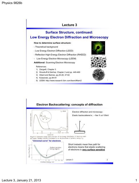
Physics 9826bLecture 3Surface Structure, continued:<strong>Low</strong> <strong>Energy</strong> <strong>Electron</strong> <strong>Diffraction</strong> <strong>and</strong> <strong>Microscopy</strong>How to determine surface structure:- Theoretical background- <strong>Low</strong> <strong>Energy</strong> <strong>Electron</strong> <strong>Diffraction</strong> (LEED)- Reflection High-<strong>Energy</strong> <strong>Electron</strong> <strong>Diffraction</strong> (RHEED)- <strong>Low</strong> <strong>Energy</strong> <strong>Electron</strong> <strong>Microscopy</strong> (LEEM)Additional: Scanning <strong>Electron</strong> <strong>Microscopy</strong>References:1) Zangwill, Chapter 32) Woodruff & Delchar, Chapter 2 <strong>and</strong> pp. 449-4603) Attard <strong>and</strong> Barnes, pp,25-28, 47-624) Kolasinski, pp.84-915) LEEM: http://www.research.ibm.com/leem/#item2Lecture 3 1<strong>Electron</strong> Backscattering: concepts of diffraction<strong>Electron</strong> diffraction <strong>and</strong> microscopy:Elastic backscattered e - , ~ few % at 100eVe“Universal curve” for electronsShort inelastic mean free path forelectrons means that elastic scatteringof electrons is very surface sensitiveLecture 3 2Lecture 3, January 21, 2013 1
Physics 9826b3.1 Real Space <strong>and</strong> Reciprocal Space Lattices- Given a unit cell with basis vectors ( a 1,a2) - There is a complementary reciprocal lattice ( a *, *) 1a2 aiaj* ij( i,j 1,2) a1* a2<strong>and</strong> a2* a1a Rectangular Lattice1 a Area of unit cell A* aa 1a*2a A |a1|| a2| sin a 2* A*|a1*||a2*|sin a *1A*Areal spaceNon-rectangular latticea 1**a 2reciprocal spacea 1**a 2reciprocal spacereal spaceLecture 3 3Substrate <strong>and</strong> Overlayer StructuresSuppose overlayer (or reconstructed surface layer) lattice different from substrateTTAB2 na1 ma nb mb121 122222a 12aOverlayer real space lattice: b1 G11a1 G12a2 b G a G aGjj*det G *a Overlayer reciprocal lattice: b1* G11*a1* G12*a2* b2* G21*a1* G22*a2*~ 1where G* G (inverse transposed matrix)GiiGij Gji*b 1det G *bb 2Lecture 3 4Lecture 3, January 21, 2013 2
Physics 9826b3.2 Reciprocal Lattice <strong>and</strong> <strong>Diffraction</strong>Recall the de Broglie relation: l Incident electronplane waved hkPeriodic arraywith direction [h k] o2kConstructive interference when path length difference = n ld (sin sin ) nl,n integerhkFor electrons :l(Å)For Heatom : l(Å)For normal incidence :od150,E(eV)0.02E(eV)hksin n~ 1- 2Å12.2E(eV )hpo150o 0, 90 , n 1:E 2dhk- as E , beam moves towards normalLecture 3 5- solution for a direction, not intensity3.3 LEED InstrumentationLEED patterns for O /Cu(001):(a) clean Cu(001); (b) p(2 1) O; (c) c(2 3)O /Cu(001)Screen-type apparatus; also measurebeam widths <strong>and</strong> intensity with Faraday cupfrom www.omicron.deGeometrical Theory of <strong>Diffraction</strong>:• Analysis of LEED beam direction (position ofspots) to give symmetry <strong>and</strong> geometry of unit cell• Strong interaction between low energy electrons<strong>and</strong> matter dynamic theory for intensities• Simplification: elastic interactions as scattering ofwaves at a 2D latticeLecture 3 6Lecture 3, January 21, 2013 3
Physics 9826bInterference ConditionsIn 1D case, interference condition is: ai(sin sino) nlk o2k ' ai (sin sin o)2(for 1D case)l na i2Periodic array with kdirection [1 0]l 2 2aik aisin o,aik' aisin ll In 2D case: a1(k ' k) 2h;h,k are integers a ( k ' k) 2k2What does this have to do with the reciprocal lattice?The equations are satisfied if:kII ( k'k)II 2( ha1 * ka2*) a k'k)II a (2h)a * a(2k) a * 21( 1 1 1 2hProve by substitution:Direction of interference maxima determined by vectors of reciprocal lattice:ghk ( ha * ka*) T *21 2 aLecture 3 7<strong>Energy</strong> <strong>and</strong> momentum conservationRecall: energy is conserved in an elastic collision:2 2 kE 2m2 2k k'or k2II k2 k'k'2IIParallel momentum is conserved in diffraction:122 ' kII kII ghk; where ghk 2( ha1* ka2*) g 2( hb * kb*)hk substrate overlayerk k IIk the LEED pattern is an image of the surface reciprocal netAside: Ewald sphere – a graphical solution to interference eq.Lecture 3 8Lecture 3, January 21, 2013 4
Physics 9826b3.4 Analysis of a simple diffraction patternSketch of diffraction pattern (reciprocal lattice):OverlayerpeaksReal space structure:Substratepeaks• Relations between overlayer <strong>and</strong> substratereciprocal lattices• Construct real-space substrate lattice• Next: construct overlayer lattice based onc(4 2)Lecture 3 9knowledge of a 1 <strong>and</strong> a 2Lecture 3 103.5 Applications <strong>and</strong> Complications of LEEDApplications of LEED:1. Surface order <strong>and</strong> cleanliness – most common2. Surface atomic structure – need theory3. Step density – get step height/density from angular beam profile (SPALLED)4. Phase transition in overlayers - structure may undergo transition withchange in coverage or T5. Dynamics of ordering, disordering, growth, phase transitions - time evolutionComplications <strong>and</strong> other aspects of LEED:1. <strong>Electron</strong> beam damage – sensitive molecular adsorbates2. Domain structure– if two domains with different structure coexist easy to distinguish– sometimes difficulties exist (e.g., 3 domains of p(2x1) on fcc(111) = (2x2)3. Transfer width (for real experimental system ~0.01, E~0.5eV)- the dimensions of ordered regions on the surface are limited to the “transferwidth” (Woodruff, p.36-37)Lecture 3, January 21, 2013 5
Physics 9826b3.6 Theory of LEED IntensitiesPositions of LEED spots give information only about surface geometry (unit cell)Need intensity analysis for determining positions of overlayer atomsKinetic Theory – “single scattering” theoryBasic assumption: electron undergoes only a single scattering event wheninteracting with ion coresOther assumptions:e Incident wave can be described by plane wave:ik ri o ik re i(After scattering, the wave from a single atom is S o f k,k ' eR R jRk’For a 2D array: I k k') Rj I FStructure factor: F SphericalwaveS22j1 Gf e i(k ' k) Rj(sum over unit cell)Lecture 3 11j2AtomicscatteringfactorInterferencefunctionPhase shiftcaused by pathdifferencebetween atom<strong>and</strong> originResults of Kinematic TheoryHow does intensity vary?- need to fulfill “Bragg condition”- no explicit E dependence, except for atomic scattering factor slow as E- theory predicts Bragg peak positions, but poorly estimates relative intensitydExample: get interference because of(i) in-plane (2D) scattering(ii) between-plane scattering = d (1 + cos ) = n lNeed multiplescattering approach!!!Lecture 3 12Lecture 3, January 21, 2013 6
Physics 9826bMultiple Scattering TheoryHighly computational; includes- ion core scattering- multiple scattering- inelastic scattering- temperature effectsEach atom experiences a flux that includes the incident flux<strong>and</strong> contributions from the other atoms• Direct (transform of diffr. int.) – highly debatable?!• Assume a trial structure, do multiple scattering calculations,use R-factor analysis(or Pendry factor; the smaller the better!!!)Lecture 3 133.7 Reflection High-<strong>Energy</strong> <strong>Electron</strong> <strong>Diffraction</strong> (RHEED)Elements of RHEED: high energy electrons (5-50keV); grazing incidence oncrystalline sample; often in Molecular Beam Epitaxy (MBE) setupscf. Luth, pp.201-209RHEED pattern consists of streaks <strong>and</strong> spots (some controversy about causes of streaks)- streaking: diffraction from perfect planes, <strong>and</strong> nearly “flat” Ewalds sphere;- spots: surface roughnessLecture 3 14Lecture 3, January 21, 2013 7
Physics 9826bExample RHEED patternsImportant use:RHEED oscillations for MBE tomonitor growth conditionsLecture 3 15Comparison of Experimental Specs for LEED <strong>and</strong> RHEEDRange of elements: all, but not element specific bothDestructive:no, except in special cases of electron-beam damage bothDepth probed: 4-20Å (LEED) 2-100Å (RHEED)Detection limits:0.1ML; atomic positions to 0.1Å bothResolving power:typically 200Å; best systems 5mm bothLateral resolution:typically 0.1mm; best systems ~10mm (LEED)200mm x 4mm; best systems 0.3nm x 6 nm (RHEED)Imaging capability:no; need special instruments – LEEMMain uses:analysis of surface crystallography (LEED)monitoring surface structure, in-situ growth (RHEED)Cost:
Physics 9826b3.8 <strong>Low</strong> <strong>Energy</strong> <strong>Electron</strong> Microscope (LEEM)LEEM history• 1962 Invention by Ernst Bauer• 1985 Operational LEEM instrument (Telieps <strong>and</strong> Bauer)• 1991 IBM LEEM-I (Tromp <strong>and</strong> Reuter)• 1998 IBM LEEM-II• 2006 SPECS FE-LEEM P90Lecture 3 17Phase contrastLecture 3 18Lecture 3, January 21, 2013 9
Physics 9826bIBM LEEM IIAfter diffraction, electrons areaccelerated from ~ 1 eV to ~10,000 eVSurf. Reviews <strong>and</strong> Lett. 5 (1998) 1189Lecture 3 19LEEM operating parameters• 0 - 100 eV electron energy• field of view 1 - 100 µm• 5 nm resolution in plane• vertical resolution: atomic steps, 0.1 nm• in situ growth, etching• RT – 1200 o C extremely useful tool to study crystal growth in situ* From R.M TrompLecture 3 20Lecture 3, January 21, 2013 10
Physics 9826b3.9 Scanning <strong>Electron</strong> <strong>Microscopy</strong> (SEM)Scanning electron microscopy (SEM)- topology, morphology, chemicalinformation (BSE <strong>and</strong> EDX)• 0.5-1000keV electron energy• field of view 0.1 - 100 µm• 5 nm resolution in plane• Magnification 10x – 300,000x• Typical operating pressure
Physics 9826bSEM/e-beam lithography in the NanofabThe e-beam lithography system (right) isa LEO 1530 field emission scanningelectron microscope (FE-SEM) fitted witha laser interferometer controlled stage(middle right).The micrograph (bottom right) shows a square array of300nm holes on 700nm pitch written in PMMA on Si.Also shown is an array of Cr dots on Si patterned by e-beam lithography <strong>and</strong> liftoff (below).http://www.uwo.ca/fab/Lecture 7 23Schematic diagram of SEMFilament (cathode): free e’s bythermionic emission of W, LaB 6Wehnelt Cylinder: focuses the e-beam <strong>and</strong> stabilizes beam currentAnode Plate: maintains the HVdifference between the anode <strong>and</strong> thecathode, <strong>and</strong> accelerates the freeelectrons down the columnCondenser Lens: reduces thediameter of the electron beam toproduce a smaller spot sizeScan Coils: electromagnetically rasterthe e-beam on the surfaceFinal Objective Lens: focuses the e-beam on the surface; the smallest spotis about 5 nm (~ 1nm with a FI source)Detectors: within the scope chamber,but not part of the column are theLecture 7 detectors24Lecture 3, January 21, 2013 12
Physics 9826bSEM DetectorsEverhart-Thornley (E-T) detectorEDX spectrometerLecture 7 25Contrast of secondary electron micrographContributions from (a) sample topography <strong>and</strong> (b) compositional contrastQ: Why do the backscattered electron micrographs, rather than secondaryelectron micrographs reveal the compositional contrast?Lecture 7 26Lecture 3, January 21, 2013 13