Chapter 5: Introduction to Computer Architecture - Edwardbosworth ...
Chapter 5: Introduction to Computer Architecture - Edwardbosworth ...
Chapter 5: Introduction to Computer Architecture - Edwardbosworth ...

You also want an ePaper? Increase the reach of your titles
YUMPU automatically turns print PDFs into web optimized ePapers that Google loves.
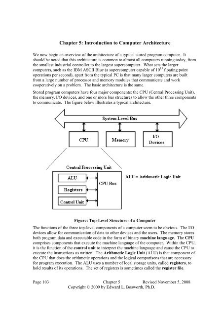
<strong>Chapter</strong> 5: <strong>Introduction</strong> <strong>to</strong> <strong>Computer</strong> <strong>Architecture</strong>We now begin an overview of the architecture of a typical s<strong>to</strong>red program computer. Itshould be noted that this architecture is common <strong>to</strong> almost all computers running <strong>to</strong>day, fromthe smallest industrial controller <strong>to</strong> the largest supercomputer. What sets the largercomputers, such as the IBM ASCII Blue (a supercomputer capable of 10 15 floating poin<strong>to</strong>perations per second), apart from the typical PC is that many larger computers are builtfrom a large number of processor and memory modules that communicate and workcooperatively on a problem. The basic architecture is the same.S<strong>to</strong>red program computers have four major components: the CPU (Central Processing Unit),the memory, I/O devices, and one or more bus structures <strong>to</strong> allow the other three components<strong>to</strong> communicate. The figure below illustrates a typical architecture.Figure: Top-Level Structure of a <strong>Computer</strong>The functions of the three <strong>to</strong>p-level components of a computer seem <strong>to</strong> be obvious. The I/Odevices allow for communication of data <strong>to</strong> other devices and the users. The memory s<strong>to</strong>resboth program data and executable code in the form of binary machine language. The CPUcomprises components that execute the machine language of the computer. Within the CPU,it is the function of the control unit <strong>to</strong> interpret the machine language and cause the CPU <strong>to</strong>execute the instructions as written. The Arithmetic Logic Unit (ALU) is that component ofthe CPU that does the arithmetic operations and the logical comparisons that are necessaryfor program execution. The ALU uses a number of local s<strong>to</strong>rage units, called registers, <strong>to</strong>hold results of its operations. The set of registers is sometimes called the register file.Page 103 <strong>Chapter</strong> 5 Revised November 5, 2008Copyright © 2009 by Edward L. Bosworth, Ph.D.
S/370 Assembler <strong>Computer</strong> Architecute & OrganizationFetch-Execute CycleAs we shall see, the fetch-execute cycle forms the basis for operation of a s<strong>to</strong>red-programcomputer. The CPU fetches each instruction from the memory unit, then executes thatinstruction, and fetches the next instruction. An exception <strong>to</strong> the “fetch next instruction” rulecomes when the equivalent of a Jump or Go To instruction is executed, in which case theinstruction at the indicated address is fetched and executed.Registers vs. MemoryRegisters and memory are similar in that both s<strong>to</strong>re data. The difference between the two issomewhat an artifact of the his<strong>to</strong>ry of computation, which has become solidified in allcurrent architectures. The basic difference between devices used as registers and devicesused for memory s<strong>to</strong>rage is that registers are faster and more expensive.In modern computers, the CPU is usually implemented on a single chip. Within this context,the difference between registers and memory is that the registers are on the CPU chip whilemost memory is on a different chip. As a result of this, the registers are not addressed in thesame way as memory – memory is accessed through an address in the MAR (more on thislater), while registers are directly addressed. Admittedly the introduction of cache memoryhas somewhat blurred the difference between registers and memory – but the addressingmechanism remains the primary difference.The CPU contains two types of registers, called special purpose registers and generalpurpose registers. The general purpose registers contain data used in computations and canbe accessed directly by the computer program. The special purpose registers are used by thecontrol unit <strong>to</strong> hold temporary results, access memory, and sequence the program execution.Normally, with one now-obsolete exception, these registers cannot be accessed by theprogram.The program status register (PSR), also called “program status word (PSW)”, is one ofthe special purpose registers found on most computers. The PSR contains a number of bits <strong>to</strong>reflect the state of the CPU as well as the result of the most recent computation. Some of thecommon bits areC the carry-out from the last arithmetic computationV Set <strong>to</strong> 1 if the last arithmetic operation resulted in an overflowN Set <strong>to</strong> 1 if the last arithmetic operation resulted in a negative numberZ Set <strong>to</strong> 1 if the last arithmetic operation resulted in a zeroI Interrupts enabled (Interrupts are discussed later)The CPU (Central Processing Unit)The CPU is that part of the computer that “does the work”. It fetches and executes themachine language that represents the program under execution. It responds <strong>to</strong> the interrupts(defined later) that usually signal Input/Output events, but which can signal issues with thememory as well as exceptions in the program execution. As indicated above, the CPU hasthree major components:1) the ALU2) the Control Unit3) the register seta) the general purpose register fileb) a number of special purpose registers used by the control unit.Page 104 <strong>Chapter</strong> 5 Revised November 5, 2008Copyright © 2009 by Edward L. Bosworth, Ph.D.
S/370 Assembler <strong>Computer</strong> Architecute & OrganizationThe ALU (Arithmetic–Logic Unit)This unit is the part of the CPU that carries out the arithmetic and logical operations of theCPU, hence its name. The ALU acts in response <strong>to</strong> control signals issued by the ControlUnit. Quite often there is an attached floating–point unit that handles all real–numberarithmetic, so it is not completely accurate <strong>to</strong> say that the ALU handles all arithmetic.The Control UnitThis unit interprets the machine language representing the computer program underexecution and issues the control signals that are necessary <strong>to</strong> achieve the effect that should beassociated with the program. This is often the most complex part of the CPU.Structure of a Typical BusA typical computer contains a number of bus structures. We have already mentioned thesystem bus and a bus internal <strong>to</strong> the CPU. Some computer designs include high-speed point<strong>to</strong>-pointbusses, used for such tasks as communication <strong>to</strong> the graphics card. In this section,we consider the structure of the system bus. The system bus is a multi-point bus that allowscommunication between a number of devices that are attached <strong>to</strong> the bus. There are twoclasses of devices that can be connected <strong>to</strong> the bus.Master DeviceSlave Devicea device that can initiate action on the bus.The CPU is always a bus master.a device that responds <strong>to</strong> requests by a bus master.Memory is an excellent example of a slave device.Devices connected <strong>to</strong> a bus are often accessed by address. System memory is a primaryexample of an addressable device; in a byte-addressable machine (more later on this),memory can be considered as an array of bytes, accessed in the same way as an array as seenin a typical programming language. I/O devices are often accessed by address; it is up <strong>to</strong> theoperating system <strong>to</strong> know the address used <strong>to</strong> access each such device.Memory Organization and AddressingWe now give an overview of RAM – Random Access Memory. This is the memory called“primary memory” or “core memory”. The term “core” is a reference <strong>to</strong> an earlier memorytechnology in which magnetic cores were used for the computer’s memory. This discussionwill pull material from a number of chapters in the textbook.Primary computer memory is best considered as an array of addressable units. Such a unit isthe smallest unit of memory that can have an independent address. In a byte–addressablememory unit, each byte (8 bits) has an independent address, although the computer oftengroups the bytes in<strong>to</strong> larger units (words, long words, etc.) and retrieves that group. Mostmodern computers manipulate integers as 32–bit (4–byte) entities, but 64–bit integers arebecoming common. Many modern designs retrieve multiple bytes at a time.Page 105 <strong>Chapter</strong> 5 Revised November 5, 2008Copyright © 2009 by Edward L. Bosworth, Ph.D.
S/370 Assembler <strong>Computer</strong> Architecute & OrganizationIn this author’s opinion, byte addressing in computers became important as the result of theuse of 8-bit character codes. Many applications involve the movement of large numbers ofcharacters (coded as ASCII or EBCDIC) and thus profit from the ability <strong>to</strong> address singlecharacters. Some computers, such as the CDC-6400, CDC-7600, and all Cray models, useword addressing. This is a result of a design decision made when considering the main goalof such computers – large computations involving floating point numbers. The word size inthese computers is 60 bits (why not 64? – I don’t know), yielding good precision for numericsimulations such as fluid flow and weather prediction.Memory as a Linear ArrayConsider a byte-addressable memory with N bytes of memory. As stated above, such amemory can be considered <strong>to</strong> be the logical equivalent of a C++ array, declared asbyte memory [N] ; // Address ranges from 0 through (N – 1)The computer on which these notes were written has 384 MB of main memory, now only anaverage size but once unimaginably large. 384 MB = 3842 20 bytes and the memory is byteaddressable,so N = 3841048576 = 402,653,184. Quite often the memory size will either bea power of two or the sum of two powers of two; 384 MB = (256 + 128)2 20 = 2 28 + 2 27 .Early versions of the IBM S/360 provided addressability of up <strong>to</strong> 2 24 = 16,777,216 bytes ofmemory, or 4,194,304 32–bit words. All addresses in the S/360 series are byte addresses.The term “random access” used when discussing computer memory implies that memorycan be accessed at random with no performance penalty. While this may not be exactly truein these days of virtual memory, the key idea is simple – that the time <strong>to</strong> access an item inmemory does not depend on the address given. In this regard, it is similar <strong>to</strong> an array inwhich the time <strong>to</strong> access an entry does not depend on the index. A magnetic tape is a typicalsequential access device – in order <strong>to</strong> get <strong>to</strong> an entry one must read over all pervious entries.There are two major types of random-access computer memory. These are:RAM Read-Write MemoryROM Read-Only MemoryThe usage of the term “RAM” for the type of random access memory that might well becalled “RWM” has a long his<strong>to</strong>ry and will be continued in this course. The basic reason isprobably that the terms “RAM” and “ROM” can easily be pronounced; try pronouncing“RWM”. Keep in mind that both RAM and ROM are random access memory.Of course, there is no such thing as a pure Read–Only memory; at some time it must bepossible <strong>to</strong> put data in the memory by writing <strong>to</strong> it, otherwise there will be no data in thememory <strong>to</strong> be read. The term “Read-Only” usually refers <strong>to</strong> the method for access by theCPU. All variants of ROM share the feature that their contents cannot be changed by normalCPU write operations. All variants of RAM (really Read-Write Memory) share the featurethat their contents can be changed by normal CPU write operations. Some forms of ROMhave their contents set at time of manufacture, other types called PROM (ProgrammableROM), can have contents changed by special devices called PROM Programmers.Page 106 <strong>Chapter</strong> 5 Revised November 5, 2008Copyright © 2009 by Edward L. Bosworth, Ph.D.
S/370 Assembler <strong>Computer</strong> Architecute & OrganizationThe Idea of Address SpaceWe now must distinguish between the idea of address space and physical memory. Theaddress space defines the range of addresses (indices in<strong>to</strong> the memory array) that can begenerated. The size of the physical memory is usually somewhat smaller, this may be bydesign (see the discussion of memory-mapped I/O below) or just by accident.The memory address is specified by a binary number placed in the Memory Address Register(MAR). The number of bits in the MAR determines the range of addresses that can begenerated. N address lines can be used <strong>to</strong> specify 2 N distinct addresses, numbered 0 through2 N – 1. This is called the address space of the computer. The early IBM S/360 had a 24–bitMAR, corresponding <strong>to</strong> an address space of 0 through 2 24 – 1, or 0 through 4,194,303.For example, we show some MAR sizes.<strong>Computer</strong> MAR bits Address RangePDP-11/20 16 0 <strong>to</strong> 65,535Intel 8086 20 0 <strong>to</strong> 1,048,575IBM 360 24 0 <strong>to</strong> 4,194,303S/370–XA 31 0 <strong>to</strong> 2,147,483,647The PDP-11/20 was an elegant smallmachine made by the now defunctDigital Equipment Corporation. Assoon as it was built, people realizedthat its address range was <strong>to</strong>o small.Pentium 32 0 <strong>to</strong> 4,294,967,295z/Series 64 A very big number.In general, the address space is muchlarger than the physical memoryavailable. For example, my personalcomputer has an address space of 2 32 (as do all Pentiums), but only 384MB = 2 28 + 2 27 bytes.Until recently the 32–bit address space would have been much larger than any possibleamount of physical memory. At present one can go <strong>to</strong> a number of companies and order acomputer with a fully populated address space; i.e., 4 GB of physical memory. Most highendpersonal computers are shipped with 1GB of memory.Word Addresses in a Byte-Addressable MachineMost computers <strong>to</strong>day, including all of those in the IBM S/360 series, have memories thatare byte-addressable; thus each byte in the memory has a unique address that can be used <strong>to</strong>address it. Under this addressing scheme, a word corresponds <strong>to</strong> a number of addresses.A 16-bit word at address Z contains bytes at addresses Z and Z + 1.A 32-bit word at address Z contains bytes at addresses Z, Z + 1, Z + 2, and Z + 3.In many computers with byte addressing, there are constraints on word addresses.A 16-bit word must have an even addressA 32-bit word must have an address that is a multiple of 4.This is true of the IBM S/360 series in which 16–bit words are called “halfwords”,32–bit words are called “words”, and 64–bit words are called “double words”. A halfwordmust have an even address, a word must have an address that is a multiple of 4 and a doubleword (64 bits) an address that is a multiple of 8.Even in computers that do not enforce this requirement, it is a good idea <strong>to</strong> observe theseword boundaries. Most compilers will do so au<strong>to</strong>matically.Page 107 <strong>Chapter</strong> 5 Revised November 5, 2008Copyright © 2009 by Edward L. Bosworth, Ph.D.
S/370 Assembler <strong>Computer</strong> Architecute & OrganizationSuppose a byte-addressable computer with a 24–bit address space. The highest byte addressis 2 24 – 1. From this fact and the address allocation <strong>to</strong> multi-byte words, we concludethe highest address for a 16-bit word is (2 24 – 2), andthe highest address for a 32-bit word is (2 24 – 4), because the 32–bit word addressed at(2 24 – 4) comprises bytes at addresses (2 24 – 4), (2 24 – 3), (2 24 – 2), and (2 24 – 1).Byte Addressing vs. Word AddressingWe have noted above that N address lines can be used <strong>to</strong> specify 2 N distinct addresses,numbered 0 through 2 N – 1. We now ask about the size of the addressable items. As asimple example, consider a computer with a 24–bit address space. The machine would have16,777,216 (16M) addressable entities. In a byte–addressable machine, such as theIBM S/360, this would correspond <strong>to</strong>:16 M Bytes 16,777,216 bytes, or8 M halfwords 8,388,608 16-bit halfwords, or4 M words 4,194,304 32–bit fullwords.The advantages of byte-addressability are clear when we consider applications that processdata one byte at a time. Access of a single byte in a byte-addressable system requires onlythe issuing of a single address. In a 16–bit word addressable system, it is necessary first <strong>to</strong>compute the address of the word containing the byte, fetch that word, and then extract thebyte from the two–byte word. Although the processes for byte extraction are wellunders<strong>to</strong>od, they are less efficient than directly accessing the byte. For this reason, manymodern machines are byte addressable.Big–Endian and Little–EndianThe reference here is <strong>to</strong> a s<strong>to</strong>ry in Gulliver’s Travels written by Jonathan Swift in which twogroups went <strong>to</strong> war over which end of a boiled egg should be broken – the big end or thelittle end. The student should be aware that Swift did not write pretty s<strong>to</strong>ries for children butfocused on biting satire; his work A Modest Proposal is an excellent example.Consider the 32-bit number represented by the eight–digit hexadecimal number 0x01020304,s<strong>to</strong>red at location Z in memory. In all byte–addressable memory locations, this number willbe s<strong>to</strong>red in the four consecutive addresses Z, (Z + 1), (Z + 2), and (Z + 3). The differencebetween big-endian and little-endian addresses is where each of the four bytes is s<strong>to</strong>red.In our example 0x01 represents bits 31 – 24,0x02 represents bits 23 – 16,0x03 represents bits 15 – 8, and0x04 represents bits 7 – 0.As a 32-bit signed integer, the number represents 01(256) 3 + 02(256) 2 + 03(256) + 04or 016 7 + 116 6 + 016 5 + 216 4 + 016 3 + 316 2 + 016 1 + 416 0 , which evaluates <strong>to</strong>116777216 + 265536 + 3256 + 41 = 16777216 + 131072 + 768 + 4 = 16909060. Notethat the number can be viewed as having a “big end” and a “little end”, as in the next figure.Page 108 <strong>Chapter</strong> 5 Revised November 5, 2008Copyright © 2009 by Edward L. Bosworth, Ph.D.
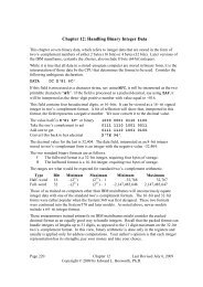
S/370 Assembler <strong>Computer</strong> Architecute & OrganizationThe “big end” contains the most significant digits of the number and the “little end” containsthe least significant digits of the number. We now consider how these bytes are s<strong>to</strong>red in abyte-addressable memory. Recall that each byte, comprising two hexadecimal digits, has aunique address in a byte-addressable memory, and that a 32-bit (four-byte) entry at address Zoccupies the bytes at addresses Z, (Z + 1), (Z + 2), and (Z + 3). The hexadecimal valuess<strong>to</strong>red in these four byte addresses are shown below.Address Big-Endian Little-EndianZ 01 04Z + 1 02 03Z + 2 03 02Z + 3 04 01The figure below shows a graphical way <strong>to</strong> view these two options for ordering the bytescopied from a register in<strong>to</strong> memory. We suppose a 32-bit register with bits numbered from31 through 0. Which end is placed first in the memory – at address Z? For big-endian, the“big end” or most significant byte is first written. For little-endian, the “little end” or leastsignificant byte is written first.Just <strong>to</strong> be complete, consider the 16-bit number represented by the four hex digits 0A0B,with decimal value 10256 + 11 = 2571. Suppose that the 16-bit word is at location W; i.e.,its bytes are at locations W and (W + 1). The most significant byte is 0x0A and the leastsignificant byte is 0x0B. The values in the two addresses are shown below.Address Big-Endian Little-EndianW 0A 0BW + 1 0B 0AHere we should note that the IBM S/360 is a “Big Endean” machine.As an example of a typical problem, let’s examine the following memory map, with byteaddresses centered on address W. Note the contents are listed as hexadecimal numbers.Each byte is an 8-bit entry, so that it can s<strong>to</strong>re unsigned numbers between 0 and 255,inclusive. These are written in hexadecimal as 0x00 through 0xFF inclusive.Address (W – 2) (W – 1) W (W + 1) (W + 2) (W + 3) (W + 4)Contents 0B AD 12 AB 34 CD EFPage 109 <strong>Chapter</strong> 5 Revised November 5, 2008Copyright © 2009 by Edward L. Bosworth, Ph.D.
S/370 Assembler <strong>Computer</strong> Architecute & OrganizationWe first ask what 32-bit integers are s<strong>to</strong>red at address W. Recalling that the value of thenumber s<strong>to</strong>red depends on whether the format is big-endian or little-endian, we draw thememory map in a form that is more useful.This figure should illustrate one obvious point: the entries (W – 2), (W – 1), and (W + 4) are“red herrings”, data that have nothing <strong>to</strong> do with the problem at hand. We now consider theconversion of the number in big-endian format. As a decimal number, this evaluates <strong>to</strong>116 7 + 216 6 + A16 5 + B16 4 + 316 3 + 416 2 + C16 1 + D, or116 7 + 216 6 + 1016 5 + 1116 4 + 316 3 + 416 2 + 1216 1 + 13, or1268435456 + 216777216 + 101048576 + 1165536 + 34096 + 4256 + 1216 + 13, or268435456 + 33554432 + 10485760 + 720896 + 12288 + 1024 + 192 + 13, or313210061.The evaluation of the number as a little–endian quantity is complicated by the fact that thenumber is negative. In order <strong>to</strong> maintain continuity, we convert <strong>to</strong> binary (recalling thatA = 1010, B = 1011, C = 1100, and D = 1101) and take the two’s-complement.Hexadecimal CD 34 AB 12Binary 11001101 00110100 10101011 00010010One’s Comp 00110010 11001011 01010100 11101101Two’s Comp 00110010 11001011 01010100 11101110Hexadecimal 32 AB 54 EEConverting this <strong>to</strong> decimal, we have the following316 7 + 216 6 + A16 5 + B16 4 + 516 3 + 416 2 + E16 1 + E, or316 7 + 216 6 + 1016 5 + 1116 4 + 516 3 + 416 2 + 1416 1 + 14, or3268435456 + 216777216 + 101048576 + 1165536 + 54096 + 4256 + 1416 + 14, or805306368 + 33554432 + 10485760 + 720896 + 20480 + 1024 + 224 + 14, or850089198The number represented in little-endian form is – 850,089,198.We now consider the next question: what 16-bit integer is s<strong>to</strong>red at address W? We beginour answer by producing the drawing for the 16-bit big-endian and little-endian numbers.Page 110 <strong>Chapter</strong> 5 Revised November 5, 2008Copyright © 2009 by Edward L. Bosworth, Ph.D.
S/370 Assembler <strong>Computer</strong> Architecute & OrganizationThe evaluation of the number as a 16-bit big-endian number is again the simpler choice. Thedecimal value is 116 3 + 216 2 + 1016 + 11 = 4096 + 512 + 160 + 11 = 4779.The evaluation of the number as a little–endian quantity is complicated by the fact that thenumber is negative. We again take the two’s-complement <strong>to</strong> convert this <strong>to</strong> positive.Hexadecimal AB 12Binary 10101011 00010010One’s Comp 01010100 11101101Two’s Comp 01010100 11101110Hexadecimal 54 EEThe magnitude of this number is 516 3 + 416 2 + 1416 + 14 = 20480 + 1024 + 224 + 14, or21742. The original number is thus the negative number – 21742.One might ask similar questions about real numbers and strings of characters s<strong>to</strong>red atspecific locations. For a string constant, the value depends on the format used <strong>to</strong> s<strong>to</strong>re stringsand might include such things as /0 termination for C and C++ strings. A typical question onreal number s<strong>to</strong>rage would be <strong>to</strong> consider the following:A real number is s<strong>to</strong>red in byte-addressable memory in little-endian form.The real number is s<strong>to</strong>red in IEEE-754 single-precision format.Address W (W + 1) (W + 2) (W + 3)Contents 00 00 E8 42The trick here is <strong>to</strong> notice that the number written in its proper form, with the “big end” onthe left hand side is 0x42E80000, which we have seen represents the number 116.00. Werethe number s<strong>to</strong>red in big-endian form, it would be a denormalized number, about 8.3210 -41 .There seems <strong>to</strong> be no advantage of one system over the other. Big-endian seems morenatural <strong>to</strong> most people and facilitates reading hex dumps (listings of a sequence of memorylocations), although a good debugger will remove that burden from all but the unlucky.Big-endian computers include the IBM 360 series, Mo<strong>to</strong>rola 68xxx, and SPARC by Sun.Little-endian computers include the Intel Pentium and related computers.Page 111 <strong>Chapter</strong> 5 Revised November 5, 2008Copyright © 2009 by Edward L. Bosworth, Ph.D.
S/370 Assembler <strong>Computer</strong> Architecute & OrganizationThe big-endian vs. little-endian debate is one that does not concern most of us directly. Letthe computer handle its bytes in any order desired as long as it produces good results. Theonly direct impact on most of us will come when trying <strong>to</strong> port data from one computer <strong>to</strong> acomputer of another type. Transfer over computer networks is facilitated by the fact that thenetwork interfaces for computers will translate <strong>to</strong> and from the network standard, which isbig-endian. The major difficulty will come when trying <strong>to</strong> read different file types.The big-endian vs. little-endian debate shows in file structures when computer data are“serialized” – that is written out a byte at a time. This causes different byte orders for thesame data in the same way as the ordering s<strong>to</strong>red in memory. The orientation of the filestructure often depends on the machine upon which the software was first developed.Any student who is interested in the literary antecedents of the terms “big-endian” and “littleendian”should read the quotation at the end of this chapter.The Control Unit“Time is nature’s way of keeping everything from happening at once”Woody AllenWe now turn our attention <strong>to</strong> a discussion of the control unit, which is that part of the CentralProcessing Unit that causes the machine language <strong>to</strong> take effect. It does this by reacting <strong>to</strong>the machine language instruction in the Instruction Register, the status flags in the ProgramStatus Register, and the interrupts in order <strong>to</strong> produce control signals that direct thefunctioning of the computer.The main strategy for the control unit is <strong>to</strong> break the execution of a machine languageinstruction in<strong>to</strong> a number of discrete steps, and then cause these primitive steps <strong>to</strong> beexecuted sequentially in the order appropriate <strong>to</strong> achieve the affect of the instruction.The System ClockThe main <strong>to</strong>ol for generating a sequence of basic execution steps is the system clock, whichgenerates a periodic signal used <strong>to</strong> generate time steps. In some designs the execution of aninstruction is broken in<strong>to</strong> major phases (e.g., Fetch and Execute), each of which is brokenin<strong>to</strong> a fixed number of minor phases that corresponds <strong>to</strong> a time signal. In other systems, theidea of major and minor phases is not much used. This figure shows a typical representationof a system clock; the CPU “speed” is just the number of clock cycles per second.The student should not be mislead in<strong>to</strong> believing that the above is an actual representation ofthe physical clock signal. A true electrical signal can never rise instantaneously or fallinstantaneously. This is a logical representation of the clock signal, showing that it changesperiodically between logic 0 and logic 1. Although the time at logic 1 is commonly the sameas the time at logic 0, this is not a requirement.Page 112 <strong>Chapter</strong> 5 Revised November 5, 2008Copyright © 2009 by Edward L. Bosworth, Ph.D.
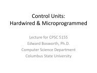
S/370 Assembler <strong>Computer</strong> Architecute & OrganizationTwo Types of Control UnitsThe function of the control unit is <strong>to</strong> emit control signals. We now ask how the control unitworks. A detailed study of the control unit should be the <strong>to</strong>pic for another course, but wemay make a few general remarks at this time.The two major classes of control unit are hardwired and microprogrammed. In ahardwired control unit, the control signals are the output of combinational logic (AND, OR,NOT gates, etc.) that has the above as input. The system clock drives a binary counter thatbreaks the execution cycle in<strong>to</strong> a number of states. As an example, there will be a fetch state,during which control signals are emitted <strong>to</strong> fetch the instruction and an execute state duringwhich control signals are emitted <strong>to</strong> execute the instruction just fetched.In a microprogrammed control unit, the control signals are the output of a register called themicro-memory buffer register. The control program (or microcode) is just a collection ofwords in the micro-memory or CROM (Control Read-Only Memory). The control unit issequenced by loading a micro-address in<strong>to</strong> the –MAR, which causes the correspondingcontrol word <strong>to</strong> be placed in<strong>to</strong> the –MBR and the control signals <strong>to</strong> be emitted.In many ways, the control program appears <strong>to</strong> be written in a very primitive machinelanguage, corresponding <strong>to</strong> a very primitive assembly language. As an example, we show asmall part of the common fetch microcode from a paper design called the Boz–5. Note thatthe memory is accessed by address and that each micro–word contains a binary number, hererepresented as a hexadecimal number. This just a program that can be changed at will,though not by the standard CPU write–<strong>to</strong>–memory instructions.Page 113 <strong>Chapter</strong> 5 Revised November 5, 2008Copyright © 2009 by Edward L. Bosworth, Ph.D.
S/370 Assembler <strong>Computer</strong> Architecute & OrganizationAddress Contents0x20 0x0010 2108 21210x21 0x0011 1500 22220x22 0x0006 4200 23230x23 0x0100 0000 0000Microprogrammed control units are more flexible than hardwired control units because theycan be changed by inserting a new binary control program. As noted in a previous chapter,this flexibility was quickly recognized by the developers of the System/360 as a significantmarketing advantage. By extending the System/360 micromemory (not a significant cost)and adding additional control code, the computer could either be run in native mode as aSystem/360, or in emulation mode as either an IBM 1401 or an IBM 7094. This ability <strong>to</strong>run the IBM 1401 and IBM 7094 executable modules with no modification simplified theprocess of upgrading computers and made the System/360 a very popular choice.It is generally agreed that the microprogrammed units are slower than hardwired units,although some writers dispute this. The disagreement lies not in the relative timings of thetwo control units, but on a critical path timing analysis of a complete CPU. It may be thatsome other part of the Fetch/Execute cycle is dominating the delays in running the program.Interrupts and Interrupt HandlingThe standard idea of a s<strong>to</strong>red program computer is that it fetches machine languageinstructions sequentially from memory and executes each in order until the program hasterminated. Such a simplistic strategy will not suffice for modern computation.Consider the case of I/O processing. Let us focus on the arrival of an Ethernet frame at theNetwork Interface Card (NIC). The data in the frame must be s<strong>to</strong>red in primary computermemory for later processing before being overwritten. In order <strong>to</strong> do this, the program underexecution must be suspended temporarily while the program controlling the NIC starts thedata transfer. The primary mechanism for suspending one program in order <strong>to</strong> executeanother program is called an interrupt.The primary rule for processing interrupts is that the execution of the interrupted programmust not be disrupted; only delayed. There is a strategy for handling interrupts that worksfor all I/O interrupts. This is a modification of the basic instruction fetch cycle. Here it is:1) At the beginning of each instruction fetch state, the status of the interrupt lineis tested. In general, this is an active–low signal.2) If the interrupt signal has been asserted, the CPU saves the current state of the CPU,which is that set of information required <strong>to</strong> restart the program as if it had not beensuspended. The CPU then fetches the first instruction of the interrupt handler routine.3) The interrupt handler identifies the source of the interrupt and calls the handlerassociated with the device that raised the interrupt.4) When the interrupt handler has finished its job, it terminates and the CPU resumesthe execution of the suspended program. Since the complete state of the suspendedprogram has been saved, it resumes execution as it nothing had happened.Page 114 <strong>Chapter</strong> 5 Revised November 5, 2008Copyright © 2009 by Edward L. Bosworth, Ph.D.
S/370 Assembler <strong>Computer</strong> Architecute & OrganizationVirtual Memory and Interrupt HandlingThere is one situation under which the above–mentioned interrupt strategy is not adequate.This occurs in a virtual memory scenario, in which a program can issue addresses that do notcorrespond <strong>to</strong> physical memory. Here are the rules:1) the program issues logical addresses,2) the address is converted <strong>to</strong> a physical address by the operating system,3) if the physical address is not in physical memory, a page fault is raised. This is aninterrupt that can occur after the instruction fetch phase has completed.Consider the execution of a memory–<strong>to</strong>–memory transfer instruction, such as an assemblylanguage instruction that might correspond <strong>to</strong> the high–level language statementY = X.The microprogram <strong>to</strong> implement this instruction might appear as follows.1. Fetch and decode the instruction.2. Compute the address for the label X and fetch the value s<strong>to</strong>red at that address.S<strong>to</strong>re that value in a temporary CPU register.3. Compute the address for the label Y and s<strong>to</strong>re the value from the temporaryCPU register in<strong>to</strong> that address.The IBM S/360 and S/370 architecture contains a number of assembly language instructionsof precisely this format. The following two instructions are rather commonly used.MVC (Move Characters) Moves a string of characters from onememory location <strong>to</strong> another.ZAP (Zero and Add Packed) Moves a sequence of packed decimal digitsfrom one memory location <strong>to</strong> another.In each scenario, the problem is the same. Here is an analysis of the above sequence.1. The instruction is fetched. If the instruction is located in a page that is not residentin primary memory, raise a page fault interrupt. This program is suspended untilthe page with the instruction is loaded in<strong>to</strong> memory. This is not a problem.2. The argumentXis fetched. If the address ofXis not resident in primary memory,raise a page fault interrupt. The program is suspended until the page with the neededdata is loaded in<strong>to</strong> memory. The instruction is restarted at step 1. Since the pagecontaining the instruction is also memory resident, this is not a problem.3. The address ofYis computed. If that address is not in primary memory, there isa problem. The instruction has already partially executed. What <strong>to</strong> do with thepartial results? In this case, the answer is quite easy, because the instruction hashad no side effects other than changing the value of a temporary register: raise apage fault interrupt, wait for the page <strong>to</strong> be loaded, and restart the instruction.The handling of such interrupts that can occur after the instruction has had other side effects,such as s<strong>to</strong>ring a partial result in<strong>to</strong> memory, can become quite complex.As an aside, the IBM S/360 did not support virtual memory, which was introduced with theS/370 in 1970.Page 115 <strong>Chapter</strong> 5 Revised November 5, 2008Copyright © 2009 by Edward L. Bosworth, Ph.D.
S/370 Assembler <strong>Computer</strong> Architecute & OrganizationInput/Output ProcessingWe now consider realistic modes of transferring data in<strong>to</strong> and out of a computer. We firstdiscuss the limitations of program controlled I/O and then explain other methods for I/O.As the simplest method of I/O, program controlled I/O has a number of shortcomings thatshould be expected. These shortcomings can be loosely grouped in<strong>to</strong> two major issues.1) The imbalance in the speeds of input and processor speeds.Consider keyboard input. An excellent typist can type about 100 words a minute (the authorof these notes was tested at 30 wpm – wow!), and the world record speeds are 180 wpm (for1 minute) in 1918 by Margaret Owen and 140 wpm (for 1 hour with an electric typewriter) in1946 by Stella Pajunas. Consider a typist who can type 120 words per minute – 2 words asecond. In the world of typing, a word is defined <strong>to</strong> be 5 characters, thus our excellent typistis producing 10 characters per second or 1 character every 100,000 microseconds. This is awaste of time; the computer could execute almost a million instructions if not waiting.2) The fact that all I/O is initiated by the CPU.The other way <strong>to</strong> state this is that the I/O unit cannot initiate the I/O. This design does notallow for alarms or error interrupts. Consider a fire alarm. It would be possible for someoneat the fire department <strong>to</strong> call once a minute and ask if there is a fire in your building; it ismuch more efficient for the building <strong>to</strong> have an alarm system that can be used <strong>to</strong> notify thefire department. Another good example is a patient moni<strong>to</strong>r that alarms if either thebreathing or heart rhythm become irregular. While such a moni<strong>to</strong>r should be polled by thecomputer on a frequent basis, it should be able <strong>to</strong> raise an alarm at any time.As a result of the imbalance in the timings of the purely electronic CPU and the electromechanicalI/O devices, a number of I/O strategies have evolved. We shall discuss these inthis chapter. All modern methods move away from the designs that cause the CPU <strong>to</strong> be theonly component <strong>to</strong> initiate I/O.The first idea in getting out of the problems imposed by having the CPU as the sole initia<strong>to</strong>rof I/O is <strong>to</strong> have the I/O device able <strong>to</strong> signal when it is ready for an I/O transaction.Specifically, we have two possibilities.1) The input device has data ready for reading by the CPU. If this is the case, the CPUcan issue an input instruction, which will be executed without delay.2) The output device can take data from the CPU, either because it can output the dataimmediately or because it can place the data in a buffer for output later. In this case,the CPU can issue an output instruction, which will be executed without delay.The idea of involving the CPU in an I/O operation only when the operation can be executedimmediately is the basis of what is called interrupt-driven I/O. In such cases, the CPUmanages the I/O but does not waste time waiting on busy I/O devices. There is anotherstrategy in which the CPU turns over management of the I/O process <strong>to</strong> the I/O device itself.In this strategy, called direct memory access or DMA, the CPU is interrupted only at thestart and termination of the I/O. When the I/O device issues an interrupt indicating that I/Omay proceed, the CPU issues instructions enabling the I/O device <strong>to</strong> manage the transfer andinterrupt the CPU upon normal termination of I/O or the occurrence of errors.Page 116 <strong>Chapter</strong> 5 Revised November 5, 2008Copyright © 2009 by Edward L. Bosworth, Ph.D.
S/370 Assembler <strong>Computer</strong> Architecute & OrganizationAn Extended (Silly) Example of I/O StrategiesThere are four major strategies that can be applied <strong>to</strong> management of the I/O process:Program-Controlled, andInterrupt-Driven, andDirect Memory Access, andI/O Channel.We try <strong>to</strong> clarify the difference between these strategies by the example of having a party inone’s house <strong>to</strong> which guests are invited. The issue here is balancing work done in the house<strong>to</strong> prepare it for the party with the tasks of waiting at the front door <strong>to</strong> admit the guests.Program-ControlledThe analogy for program-controlled I/O would be for the host <strong>to</strong> remain at the door,constantly looking out, and admitting guests as each one arrives. The host would be at thedoor constantly until the proper number of guests arrived, at which time he or she couldcontinue preparations for the party. While standing at the door, the host could do no otherproductive work. Most of us would consider that a waste of time.Interrupt-DrivenMany of us have solved this problem by use of an interrupt mechanism called a doorbell.When the doorbell rings, the host suspends the current task and answers the door. Havingadmitted the guest, the host can then return <strong>to</strong> preparations for the party. Note that thisexample contains, by implication, several issues associated with interrupt handling.The first issue is priority. If the host is in the process of putting out a fire in the kitchen, heor she may not answer the door until the fire is suppressed. A related issue is necessarycompletion. If the host has just taken a cake out of the oven, he or she will not drop the cakeon the floor <strong>to</strong> answer the door, but will first put the cake down on a safe place and thenproceed <strong>to</strong> the door. In this scenario, the host’s time is spent more efficiently as he or shespends little time actually attending the door and can spend most of the time in productivework on the party.Direct Memory AccessIn this case, the host unlocks the door and places a note on it indicating that the guests shouldjust open the door and come in. The host places a number of tickets at the door, one for eachguest expected, with a note that the guest taking the last ticket should so inform the host.When the guest taking the last ticket has arrived, the host is notified and locks the door. Inthis example the host’s work is minimized by removing the requirement <strong>to</strong> go <strong>to</strong> the door foreach arrival of a guest. There are only two trips <strong>to</strong> the door, one at the beginning <strong>to</strong> set up forthe arrival of guests and one at the end <strong>to</strong> close the door.I/O ChannelThe host hires a butler <strong>to</strong> attend the door and lets the butler decide the best way <strong>to</strong> do it. Thebutler is expected <strong>to</strong> announce when all the guests have arrived.Note that the I/O channel is not really a distinct strategy. Within the context of our sillyexample, we note that the butler will use one of the above three strategies <strong>to</strong> admit guests.The point of the strategy in this context is that the host is relieved of the duties. In the realworld of computer I/O, the central processor is relieved of most I/O management duties.Page 117 <strong>Chapter</strong> 5 Revised November 5, 2008Copyright © 2009 by Edward L. Bosworth, Ph.D.
S/370 Assembler <strong>Computer</strong> Architecute & OrganizationImplementation of I/O StrategiesWe begin our brief discussion of physical I/O by noting that it is based on interaction of aCPU and a set of registers associated with the I/O device. In general, each I/O device hasthree types of registers associated with it: data, control, and status. From the view of aprogrammer, the I/O device can be almost completely characterized by these registers,without regard <strong>to</strong> the actual source or destination of the data.For this section, we shall imagine a hopelessly simplistic computer with a single CPUregister, called the ACC (accumula<strong>to</strong>r) and four instructions. These instructions are:1. LOAD Address Loads the accumula<strong>to</strong>r from the memory address,2. STORE Address S<strong>to</strong>res the accumula<strong>to</strong>r contents in<strong>to</strong> the memory address,3. GET Register Loads the accumula<strong>to</strong>r from the I/O register, and4. PUT Register S<strong>to</strong>res the accumula<strong>to</strong>r contents in<strong>to</strong> the I/O register.The best way <strong>to</strong> understand IBM’s rationale for its I/O architecture <strong>to</strong> consider some simplerdesigns that might have been chosen. We begin with a very primitive I/O scheme.The First Idea, and Why It Cannot WorkAt first consideration, I/O in a computer system would appear trivial. We just issue theinstructions and access the data register by address, so that we have:GET TEXT_IN_DATA -- this reads from the input unit.PUT TEXT_OUT_DATA -- this writes <strong>to</strong> the output unit.Strictly speaking, these instructions operate as advertised in the code fragments above. Wenow expose the difficulties, beginning with the input problem. The input unit is connected <strong>to</strong>the CPU through the register at address TEXT_IN_DATA. Loading a CPU from that inputregister will always transfer some data, but might not transfer what we want. Normally, weexpect an input request <strong>to</strong> wait until a character has been input by the user and only thentransfer the character <strong>to</strong> the CPU. As written above, the instruction just copies what is in thedata buffer of the input unit; it might be user data or it might be garbage left over frominitialization. We must find a way <strong>to</strong> command the unit <strong>to</strong> read, wait for a new character <strong>to</strong>have been input, and only then transfer the data <strong>to</strong> the CPU.The output instruction listed above might as well be stated as “Just throw it over the wall andhope someone catches it.” We are sending data <strong>to</strong> the output unit without first testing <strong>to</strong> seeif the output unit is ready for data. Early in his career as a programmer, this author wrote aprogram that sent characters <strong>to</strong> a teletype printer faster than they could be printed; the resultwas that each character printed was a combination of two or more characters actually sent <strong>to</strong>the TTY, and none were actually correct. As this was the intended result of this experiment,this author was pleased and determined that he had learned something.The solution <strong>to</strong> the problem of actually being able <strong>to</strong> do input and output correctly is basedon the proper use of these two instructions. The solution we shall describe is called programcontrolled I/O. We shall first describe the method and then note its shortcomings.Page 118 <strong>Chapter</strong> 5 Revised November 5, 2008Copyright © 2009 by Edward L. Bosworth, Ph.D.
S/370 Assembler <strong>Computer</strong> Architecute & OrganizationThe basic idea for program–controlled I/O is that the CPU initiates all input and outpu<strong>to</strong>perations. The CPU must test the status of each device before attempting <strong>to</strong> use it and issuean I/O command only when the device is ready <strong>to</strong> accept the command. The CPU thencommands the device and continually checks the device status until it detects that the deviceis ready for an I/O event. For input, this happens when the device has new data in its databuffer. For output, this happens when the device is ready <strong>to</strong> accept new data.Pure program–controlled I/O is feasible only when working with devices that are alwaysinstantly ready <strong>to</strong> transfer data. For example, we might use program–controlled input <strong>to</strong> readan electronic gauge. Every time we read the gauge, the CPU will get a value. While thissolution is not without problems, it does avoid the busy wait problem.The “busy wait” problem occurs when the CPU executes a tight loop doing nothing exceptwaiting for the I/O device <strong>to</strong> complete its transaction. Consider the example of a fast typistinputting data at the rate of one character per 100,000 microseconds. The busy wait loop willexecute about one million times per character input, just wasting time. The shortcomings ofsuch a method are obvious (IBM had observed them in the late 1940’s).As a result of the imbalance in the timings of the purely electronic CPU and the electro–mechanical I/O devices, a number of I/O strategies have evolved. We shall discuss these inthis chapter. All modern methods move away from the designs that cause the CPU <strong>to</strong> be theonly component <strong>to</strong> initiate I/O.The idea of involving the CPU in an I/O operation only when the operation can be executedimmediately is the basis of what is called interrupt-driven I/O. In such cases, the CPUmanages the I/O but does not waste time waiting on busy I/O devices. There is anotherstrategy in which the CPU turns over management of the I/O process <strong>to</strong> the I/O device itself.In this strategy, called direct memory access or DMA, the CPU is interrupted only at thestart and termination of the I/O. When the I/O device issues an interrupt indicating that I/Omay proceed, the CPU issues instructions enabling the I/O device <strong>to</strong> manage the transfer andinterrupt the CPU upon normal termination of I/O or the occurrence of errors.Interrupt Driven I/OHere the CPU suspends the program that requests the Input and activates another process.While this other process is being executed, the input device raises 80 interrupts, one for eachof the characters input. When the interrupt is raised, the device handler is activated for thevery short time that it takes <strong>to</strong> copy the character in<strong>to</strong> a buffer, and then the other process isactivated again. When the input is complete, the original user process is resumed.In a time–shared system, such as all of the S/370 and successors, the idea of an interruptallows the CPU <strong>to</strong> continue with productive work while a program is waiting for data. Hereis a rough scenario for the sequence of events following an I/O request by a user job.1. The operating system commands the operation on the selected I/O device.2. The operating system suspends execution of the job, places it on a wait queue,and assigns the CPU <strong>to</strong> another job that is ready <strong>to</strong> run.3. Upon completion of the I/O, the device raises an interrupt. The operating systemhandles the interrupt and places the original job in a queue, marked as ready <strong>to</strong> run.4. At some time later, the job will be run.Page 119 <strong>Chapter</strong> 5 Revised November 5, 2008Copyright © 2009 by Edward L. Bosworth, Ph.D.
S/370 Assembler <strong>Computer</strong> Architecute & OrganizationIn order <strong>to</strong> consider the next refinement of the I/O structure, let us consider what we havediscussed previously. Suppose that a line of 80 typed characters is <strong>to</strong> be input.Interrupt DrivenHere the CPU suspends the program that requests the Input and activates another process.While this other process is being executed, the input device raises 80 interrupts, one for eachof the characters input. When the interrupt is raised, the device handler is activated for thevery short time that it takes <strong>to</strong> copy the character in<strong>to</strong> a buffer, and then the other process isactivated again. When the input is complete, the original user process is resumed.Direct Memory AccessDMA is a refinement of interrupt-driven I/O in that it uses interrupts at the beginning andend of the I/O, but not during the transfer of data. The implication here is that the actualtransfer of data is not handled by the CPU (which would do that by processing interrupts),but by the I/O controller itself. This removes a considerable burden from the CPU.In the DMA scenario, the CPU suspends the program that requests the input and againactivates another process that is eligible <strong>to</strong> execute. When the I/O device raises an interruptindicating that it is ready <strong>to</strong> start I/O, the other process is suspended and an I/O processbegins. The purpose of this I/O process is <strong>to</strong> initiate the device I/O, after which the otherprocess is resumed. There is no interrupt again until the I/O is finished.The design of a DMA controller then involves the development of mechanisms by which thecontroller can communicate directly with the computer’s primary memory. The controllermust be able <strong>to</strong> assert a memory address, specify a memory READ or memory WRITE, andaccess the primary data register, called the MBR (Memory Buffer Register).Immediately, we see the need for a bus arbitration strategy – suppose that both the CPUand a DMA controller want <strong>to</strong> access the memory at the same time. The solution <strong>to</strong> thisproblem is called “cycle stealing”, in which the CPU is blocked for a cycle from accessingthe memory in order <strong>to</strong> give preference <strong>to</strong> the DMA device.Any DMA controller must contain at least four registers used <strong>to</strong> interface <strong>to</strong> the system bus.1) A word count register (WCR) – indicating how many words <strong>to</strong> transfer.2) An address register (AR) – indicating the memory address <strong>to</strong> be used.3) A data buffer.4) A status register, <strong>to</strong> allow the device status <strong>to</strong> be tested by the CPU.In essence, the CPU tells the DMA controller “Since you have interrupted me, I assume thatyou are ready <strong>to</strong> transfer data. Transfer this amount of data <strong>to</strong> or from the memory blockbeginning at this memory address and let me know when you are done or have a problem.”Page 120 <strong>Chapter</strong> 5 Revised November 5, 2008Copyright © 2009 by Edward L. Bosworth, Ph.D.
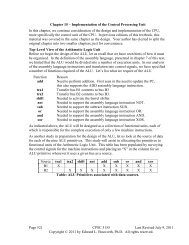
S/370 Assembler <strong>Computer</strong> Architecute & OrganizationI/O ChannelA channel is a separate special-purpose computer that serves as a sophisticated DirectMemory Access device controller. It directs data between a number of I/O devices and themain memory of the computer. Generally, the difference is that a DMA controller willhandle only one device, while an I/O channel will handle a number of devices.The I/O channel concept was developed by IBM (the International Business MachineCorporation) in the 1940’s because it was obvious even then that data Input/Output might bea real limit on computer performance if the I/O controller were poorly designed. By the IBMnaming convention, I/O channels execute channel commands, as opposed <strong>to</strong> instructions.There are two types of channels – multiplexer and selec<strong>to</strong>r.A multiplexer channel supports more than one I/O device by interleaving the transfer ofblocks of data. A byte multiplexer channel will be used <strong>to</strong> handle a number of low-speeddevices, such as printers and terminals. A block multiplexer channel is used <strong>to</strong> supporthigher-speed devices, such as tape drives and disks.A selec<strong>to</strong>r channel is designed <strong>to</strong> handle high speed devices, one at a time. This type ofchannel became largely disused prior <strong>to</strong> 1980, probably replaced by blocked multiplexers.Each I/O channel is attached <strong>to</strong> one or more I/O devices through device controllers that aresimilar <strong>to</strong> those used for Interrupt-Driven I/O and DMA, as discussed above.I/O Channels, Control Units, and I/O DevicesPage 121 <strong>Chapter</strong> 5 Revised November 5, 2008Copyright © 2009 by Edward L. Bosworth, Ph.D.
S/370 Assembler <strong>Computer</strong> Architecute & OrganizationIn one sense, an I/O channel is not really a distinct I/O strategy, due <strong>to</strong> the fact that an I/Ochannel is a special purpose processor that uses either Interrupt-Driven I/O or DMA <strong>to</strong> affectits I/O done on behalf of the central processor. This view is unnecessarily academic.In the IBM System-370 architecture, the CPU initiates I/O by executing a specific instructionin the CPU instruction set: EXCP for Execute Channel Program. Channel programs areessentially one word programs that can be “chained” <strong>to</strong> form multi-command sequences.Physical IOCSThe low level programming of I/O channels, called PIOCS for Physical I/O Control System,provides for channel scheduling, error recovery, and interrupt handling. At this level, the onewrites a channel program (one or more channel command words) and synchronizes the mainprogram with the completion of I/O operations. For example, consider double-buffered I/O,in which a data buffer is filled and then processed while another data buffer is being filled. Itis very important <strong>to</strong> verify that the buffer has been filled prior <strong>to</strong> processing the data in it.In the IBM PIOCS there are four major macros used <strong>to</strong> write the code.CCW Channel Command WordThe CCW macro causes the IBM assembler <strong>to</strong> construct an 8-byte channel command word.The CCW includes the I/O command code (1 for read, 2 for write, and other values), the startaddress in main memory for the I/O transfer, a number of flag bits, and a count field.EXCP Execute Channel ProgramThis macro causes the physical I/O system <strong>to</strong> start an I/O operation. This macro takes as itssingle argument the address of a block of channel commands <strong>to</strong> be executed.WAITThis synchronizes main program execution with the completion of an I/O operation. Thismacro takes as its single argument the address of the block of channel commands for which itwill wait.ChainingThe PIOCS provides a number of interesting chaining options, including command chaining.By default, a channel program comprises only one channel command word. To execute morethan one channel command word before terminating the I/O operation, it is necessary <strong>to</strong>chain each command word <strong>to</strong> the next one in the sequence; only the last command word inthe block does not contain a chain bit.Here is a sample of I/O code.The main I/O code is as follows. Note that the program waits for I/O completion.// First execute the channel program at address INDEVICE.EXCP INDEVICE// Then wait <strong>to</strong> synchronize program execution with the I/OWAIT INDEVICE// Fill three arrays in sequence, each with 100 bytes.INDEVICE CCW 2, ARRAY_A, X’40’, 100CCW 2, ARRAY_B, X’40’, 100CCW 2, ARRAY_C, X’00’, 100Page 122 <strong>Chapter</strong> 5 Revised November 5, 2008Copyright © 2009 by Edward L. Bosworth, Ph.D.
S/370 Assembler <strong>Computer</strong> Architecute & OrganizationThe first number in the CCW (channel command word) is the command code indicating theoperation <strong>to</strong> be performed; e.g., 1 for write and 2 for read. The hexadecimal 40 in the CCWis the “chain command flag” indicating that the commands should be chained. Note that thelast command in the list has a chain command flag set <strong>to</strong> 0, indicating that it is the last one.Front End ProcessorWe can push the I/O design strategy one step further – let another computer handle it. Oneexample that used <strong>to</strong> be common occurred when the IBM 7090 was introduced. At the time,the IBM 1400 series computer was quite popular. The IBM 7090 was designed <strong>to</strong> facilitatescientific computations and was very good at that, but it was not very good at I/O processing.As the IBM 1400 series excelled at I/O processing it was often used as an I/O front-endprocessor, allowing the IBM 7090 <strong>to</strong> handle I/O only via tape drives.The batch scenario worked as follows:1) Jobs <strong>to</strong> be executed were “batched” via the IBM 1401 on<strong>to</strong> magnetic tape. Thisscenario did not support time sharing.2) The IBM 7090 read the tapes, processed the jobs, and wrote results <strong>to</strong> tape.3) The IBM 1401 read the tape and output the results as indicated. This outputincluded program listings and any data output required.Another system that was in use was a combined CDC 6400/CDC 7600 system (withcomputers made by Control Data Corporation), in which the CDC 6400 operated as an I/Ofront-end and wrote <strong>to</strong> disk files for processing by the CDC 7600. This combination was inaddition <strong>to</strong> the fact that each of the CDC 6400 and CDC 7600 had a number of IOPS (I/OProcessors) that were essentially I/O channels as defined by IBM.Page 123 <strong>Chapter</strong> 5 Revised November 5, 2008Copyright © 2009 by Edward L. Bosworth, Ph.D.
S/370 Assembler <strong>Computer</strong> Architecute & OrganizationGulliver’s Travels and “Big-Endian” vs. “Little-Endian”The author of these notes has been <strong>to</strong>ld repeatedly of the literary antecedents of the terms“big-endian” and “little-endian” as applied <strong>to</strong> byte ordering in computers. In a fit ofscholarship, he decided <strong>to</strong> find the original quote. Here it is, taken from <strong>Chapter</strong> IV of Part I(A Voyage <strong>to</strong> Lilliput) of Gulliver’s Travels by Jonathan Swift, published Oc<strong>to</strong>ber 28, 1726.The edition consulted for these notes was published in 1958 by Random House, Inc. as a par<strong>to</strong>f its “Modern Library Books” collection. The LC Catalog Number is 58-6364.The s<strong>to</strong>ry of “big-endian” vs. “little-endian” is described in the form on a conversationbetween Gulliver and a Lilliputian named Reldresal, the Principal Secretary of PrivateAffairs <strong>to</strong> the Emperor of Lilliput. Reldresal is presenting a his<strong>to</strong>ry of a number of strugglesin Lilliput, when he moves from one difficulty <strong>to</strong> another. The following quote preserves theunusual capitalization and punctuation found in the source material.“Now, in the midst of these intestine Disquiets, we are threatened with anInvasion from the Island of Blefuscu, which is the other great Empire of theUniverse, almost as large and powerful as this of his majesty. ….[The two great Empires of Lilliput and Blefuscu] have, as I was going <strong>to</strong> tell you,been engaged in a most obstinate War for six and thirty Moons past. It beganupon the following Occasion. It is allowed on all Hands, that the primitive Wayof breaking Eggs before we eat them, was upon the larger End: But his presentMajesty’s Grand-father, while he was a Boy, going <strong>to</strong> eat an Egg, and breaking itaccording <strong>to</strong> the ancient Practice, happened <strong>to</strong> cut one of his Fingers.Whereupon the Emperor his Father, published an Edict, commanding all hisSubjects, upon great Penalties, <strong>to</strong> break the smaller End of their Eggs. ThePeople so highly resented this Law, that our His<strong>to</strong>ries tell us, there have been sixRebellions raised on that Account; wherein one Emperor lost his Life, andanother his Crown. These civil Commotions were constantly fomented by theMonarchs of Blefuscu; and when they were quelled, the Exiles always fled forRefuge <strong>to</strong> that Empire. It is computed, that eleven Thousand Persons have, atseveral Times, suffered Death, rather than submit <strong>to</strong> break their Eggs at thesmaller end. Many hundred large Volumes have been published upon thisControversy: But the Books of the Big-Endians have been long forbidden, andthe whole Party rendered incapable by Law of holding Employments.”Jonathan Swift was born in Ireland in 1667 of English parents. He <strong>to</strong>ok a B.A. at TrinityCollege in Dublin and some time later was ordained an Anglican priest, serving briefly in aparish church, and became Dean of St. Patrick’s in Dublin in 1713. Contemporary criticsconsider the Big-Endians and Little-Endians <strong>to</strong> represent Roman Catholics and Protestantsrespectively. Lilliput seems <strong>to</strong> represent England, and its enemy Blefuscu is variouslyconsidered <strong>to</strong> represent either France or Ireland. Note that the phrase “little-endian” seemsnot <strong>to</strong> appear explicitly in the text of Gulliver’s Travels.Page 124 <strong>Chapter</strong> 5 Revised November 5, 2008Copyright © 2009 by Edward L. Bosworth, Ph.D.