Adobe PDF - Edwardbosworth.com
Adobe PDF - Edwardbosworth.com
Adobe PDF - Edwardbosworth.com

You also want an ePaper? Increase the reach of your titles
YUMPU automatically turns print PDFs into web optimized ePapers that Google loves.
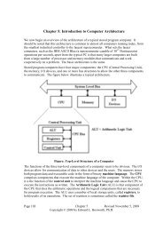
Chapter 15 – Implementation of the Central Processing Unit<br />
In this chapter, we continue consideration of the design and implementation of the CPU,<br />
more specifically the control unit of the CPU. In previous editions of this textbook, this<br />
material was covered in the same chapter as the design. Your author has elected to split the<br />
original chapter into two smaller chapters, just for convenience.<br />
Top-Level View of the Arithmetic-Logic Unit<br />
Before we begin the design of the ALU, let us recall that we have seen hints of how it must<br />
be organized. In the definition of the assembly language, presented in chapter 7 of this text,<br />
we hinted that the ALU would be divided into a number of execution units. In our analysis<br />
of the assembly language instructions and translation into control signals, we have specified<br />
a number of functions required of the ALU. Let’s list what we require of the ALU.<br />
Function Reason<br />
add Need to perform addition. First seen in the need to update the PC,<br />
this also supports the ADD assembly language instruction.<br />
tra1 Transfer bus B1 contents to bus B3<br />
tra2 Transfer bus B2 contents to bus B3.<br />
shift Needed to activate the barrel shifter<br />
not Needed to support the assembly language instruction NOT.<br />
sub Needed to support the subtract instruction SUB.<br />
or Needed to support the assembly language instruction OR.<br />
and Needed to support the assembly language instruction AND.<br />
xor Needed to support the assembly language instruction XOR.<br />
As indicated above, the ALU will be designed as a collection of functional units, each of<br />
which is responsible for the <strong>com</strong>plete execution of only a few machine instructions.<br />
As another study in preparation for the design of the ALU, let us look at the source of data<br />
for each of the nine ALU primitives. This study will assist in allocating the primitives to<br />
functional units of the Arithmetic Logic Unit. This table has been populated by surveying<br />
the control signals for the machine instructions and placing an “X” in the column for an<br />
ALU primitive whenever it uses a given bus as a source.<br />
Source tra1 tra2 shift not add sub or and xor<br />
B1 X X X X X X<br />
B2 X X X X X X X X<br />
Table: ALU Primitives associated with data sources.<br />
Page 521 CPSC 5155 Last Revised July 9, 2011<br />
Copyright © 2011 by Edward L. Bosworth, Ph.D. All rights reserved.
Chapter 15 Boz–7 Implementation of the CPU<br />
The above two analyses indicate a simple division of the ALU into four primitive units.<br />
TRA / NOT this handles the tra1, tra2, and not primitives,<br />
SHIFT this is the barrel shifter; it handles the shift primitives,<br />
ADD / SUB this handles addition and subtraction, and<br />
LOGICAL this handles the logical operations: or, and, xor.<br />
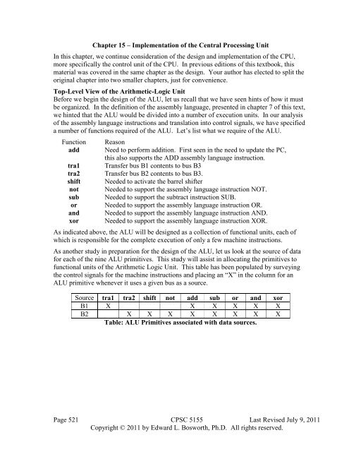
Here then is the top-level ALU design.<br />
Note that each of buses B1 and B2 feed<br />
all of the units except the barrel shifter,<br />
which is fed only by bus B3. All units<br />
output on bus B3 and are connected by<br />
tri-state units, so that bus conflicts do<br />
not occur. For this first unit, we have<br />
tra1 input from B1<br />
tra2 input from B2<br />
not input from B1<br />
The Logical Unit contains those<br />
Boolean functions that take two inputs.<br />
These are AND, OR, and XOR.<br />
Although the NOT is also a Boolean<br />
function, it is more easily placed in the<br />
first unit.<br />
The Adder/Subtractor unit is also a<br />
binary unit and might be placed with the<br />
Logical Unit, except that such a design<br />
would appear more <strong>com</strong>plicated than<br />
necessary. We design this unit as a<br />
standalone module.<br />
The Barrel Shifter accepts input only<br />
from bus B2. We have seen its design<br />
earlier, with the input labeled X 31-0 and<br />
the output labeled Y 31-0 .<br />
Figure: Top-Level ALU Design.<br />
The above control signals are generally required to be mutually exclusive in order for the<br />
ALU to function correctly. Of the set {tra1, tra2, not, or, and, xor, add, sub, shift} at most<br />
one may be active during any clock pulse or the ALU will malfunction. The three shift<br />
mode selectors (A, C, and L / R ) may be asserted in any <strong>com</strong>bination (though A = 1 and C =<br />
1 is arbitrarily changed to A = 0 and C = 1) and have effect only when shift = 1.<br />
Page 522 CPSC 5155 Last Revised July 9, 2011<br />
Copyright © 2011 by Edward L. Bosworth, Ph.D. All rights reserved.
Chapter 15 Boz–7 Implementation of the CPU<br />
The TRA / NOT Unit<br />
The design of this unit is particularly simple. We present the design for a single bit and note<br />
that the <strong>com</strong>plete design just replicates this 32 times. In this and other figures B1 K refers to<br />
bit K on bus B1, B2 K to bit K on bus B2, and B3 K to bit K on bus B3, with 0 K 31. Note<br />
the extensive use of tri-state buffers to connect output to bus B3.<br />
Figure: The TRA/NOT Unit<br />
The Binary Logical Unit<br />
The design of this unit is also particularly simple. Again, we show the design for just one<br />
bit and note that the <strong>com</strong>plete design replicates this 32 times.<br />
Figure: The Binary Logical Unit<br />
Page 523 CPSC 5155 Last Revised July 9, 2011<br />
Copyright © 2011 by Edward L. Bosworth, Ph.D. All rights reserved.
Chapter 15 Boz–7 Implementation of the CPU<br />
The Add/Subtract Unit<br />
To avoid additional <strong>com</strong>plexity, we implement this unit as a 32-bit ripple-carry unit.<br />
Figure: High and Lower Order Bits of an Adder/Subtractor, with Overflow Bit V<br />
The Shifter Unit<br />
All we do here is to attach the shifter to buses B2 and B3.<br />
Figure: The Shifter Unit<br />
Page 524 CPSC 5155 Last Revised July 9, 2011<br />
Copyright © 2011 by Edward L. Bosworth, Ph.D. All rights reserved.
Chapter 15 Boz–7 Implementation of the CPU<br />
The State Registers<br />
We now consider the two state registers used in the hardwired control unit. These are the<br />
minor state register (responsible for the four pulses T0, T1, T2, and T3) and the major<br />
state register (responsible for transitions between the three major states: F, D, and A).<br />
The Minor State Register<br />
The minor state register will be a modulo–4 counter, implemented as a one-hot design using<br />
four D flip-flops. Because of the close association, we shall also show the RUN flip-flop.<br />
Figure: The Minor State Register with the Run Flip-Flop<br />
Note that when RUN = 0, the system clock does not reach the minor state register, which<br />
remains frozen in its last state until the system is restarted. The Start signal is used to reset<br />
the minor state register to T 0 = 1. The state register is a four-bit circular shift register.<br />
This style of shift register is called “one hot” because, at any given time, only one flip–flop<br />
has value 1 and the rest are set to 0. A design with two flip–flops and a 2–to–4 decoder<br />
could perform an equivalent function, though with time delays for the state decoding.<br />
The Major State Register<br />
The function of the major state register is to control the execution state of the machine<br />
language instructions. The current design has 3 major states: Fetch, Defer, and Execute.<br />
The design of this register is simplified by the fact that almost all of the instructions execute<br />
in the Fetch cycle. Only eight instructions (GET, PUT, RET, RTI, LDR, STR, BR, and<br />
JSR) even enter the Execute state, much less the Defer state. Recall that GET, PUT, RET,<br />
and RTI cannot enter the Defer stage and that the others enter it only if IR 26 = 1.<br />
Page 525 CPSC 5155 Last Revised July 9, 2011<br />
Copyright © 2011 by Edward L. Bosworth, Ph.D. All rights reserved.
Chapter 15 Boz–7 Implementation of the CPU<br />
In the next table, we examine these instructions closely to determine patterns that will be of<br />
use in defining the Major State Register. For all other instructions, the state after Fetch is<br />
Fetch again; the instruction <strong>com</strong>pletes execution in one major cycle and the next is fetched.<br />
IR 31 IR 30 IR 29 IR 28 IR 27 IR 26 = 0 IR 26 = 1<br />
GET 0 1 0 0 0 Execute<br />
PUT 0 1 0 0 1 Execute<br />
RET 0 1 0 1 0 Execute<br />
RTI 0 1 0 1 1 Execute<br />
LDR 0 1 1 0 0 Execute Defer<br />
STR 0 1 1 0 1 Execute Defer<br />
JSR 0 1 1 1 0 Execute Defer<br />
BR 0 1 1 1 1 Execute if Branch = 1,<br />
Fetch Otherwise<br />
Defer if Branch = 1,<br />
Fetch Otherwise<br />
We define two generated control signals, S 1 and S 2 , as follows:<br />
1. If the present state is Fetch and S 1 = = 0, the next state will be Fetch.<br />
If the present state is Fetch and S 1 = = 1, the next state is either Defer or Execute.<br />
2. If the present state is Fetch, S 1 = = 1, and S 2 = = 0, the next state will be Execute.<br />
If the present state is Fetch, S 1 = = 1, and S 2 = = 1, the next state will be Defer.<br />
3. Automatic rule: If the present state is Defer, the next state will be Execute.<br />
4. Automatic rule: If the present state is Execute, the next state will be Fetch.<br />
This leads to the following state diagram for the Major State Register.<br />
Figure: State Diagram for the Major State Register<br />
A three–state diagram requires two flip–flops for its implementation. To begin this design,<br />
we assign two–bit binary numbers, denoted Y 1 Y 0 , to each of the major states.<br />
State Y 1 Y 0<br />
F 0 0<br />
D 0 1<br />
E 1 0<br />
Page 526 CPSC 5155 Last Revised July 9, 2011<br />
Copyright © 2011 by Edward L. Bosworth, Ph.D. All rights reserved.
Chapter 15 Boz–7 Implementation of the CPU<br />
The easiest way to implement this design uses two D flip–flops, with inputs D 1 and D 0 . We<br />
are now left with only two questions:<br />
1. How to generate the two inputs D 1 and D 0 from S 1 , S 2 , Y 0 , and Y 1 .<br />
2. How to generate S 1 and S 2 from the op–codes.<br />
It will be seen below that the circuitry to generate these signals is quite simple. We first ask<br />
ourselves how it came to be so simple when it had the possibility of great <strong>com</strong>plexity. To<br />
see what has happened, we examine the evolution of the op–codes for the first 12<br />
instructions.<br />
Op-Code Version 1 Version 2 Version 3 Version 4<br />
00 000 HLT HLT HLT HLT<br />
00 001 LDI LDI LDI LDI<br />
00 010 ANDI ANDI ANDI ANDI<br />
00 011 ADDI ADDI ADDI ADDI<br />
00 100 GET<br />
00 101 PUT<br />
00 110 LDR<br />
00 111 STR<br />
01 000 BR GET GET GET<br />
01 001 JSR PUT PUT PUT<br />
01 010 RET LDR RET RET<br />
01 011 RTI STR RTI RTI<br />
01 100 BR LDR LDR<br />
01 101 JSR STR STR<br />
01 110 RET BR JSR<br />
01 111 RTI JSR BR<br />
In each of these designs, the four “immediate instructions” are allocated the first 4 op–codes,<br />
numbered 0 through 3. The original idea was that all such instructions would have op–codes<br />
beginning with “000”. This was a good idea, but has yet to be exploited in these designs.<br />
Version 1 of the list of instructions just presented the instructions in the way the author<br />
thought them up. The instructions were considered to exist in four groups: GET & PUT;<br />
LDR & STR; JSR, RET, & RTI; and BR. They were listed in that order, with the exception<br />
that the BR was listed first, because early designs did not allow for subroutine calls. This<br />
almost–random order of op–codes yielded a very messy control unit.<br />
Version 2 of this list resulted from the observation that introducing four NOP instructions<br />
and moving the instructions beginning with GET down by four would yield the result that all<br />
instructions that could leave the Fetch state would have op–codes beginning with “01”. This<br />
decision was taken because it introduced a regularity into the pattern of op–codes and this<br />
author expected such a pattern to yield a simplification in the circuitry.<br />
Version 3 of the list resulted from the observation that moving the RET and RTI<br />
instructions to follow GET and PUT would yield the result that those instructions that might<br />
use the Defer state all began with “011”.<br />
Page 527 CPSC 5155 Last Revised July 9, 2011<br />
Copyright © 2011 by Edward L. Bosworth, Ph.D. All rights reserved.
Chapter 15 Boz–7 Implementation of the CPU<br />
Version 4 of the list is a minor modification of version 3. It is a result of the observation<br />
that the branch instruction, BR, is the only one that has an additional constraint on its<br />
leaving the Fetch state. It leaves Fetch if and only if the signal Branch = = 1. This is a time<br />
saving feature that avoids <strong>com</strong>putation of an effective address when the branch is not going<br />
to be taken. For this reason, the BR instruction was moved to last in the list.<br />
We now repeat the table that began this discussion and recall the definition of the two<br />
generated control signals S 1 and S 2 .<br />
IR 31 IR 30 IR 29 IR 28 IR 27 IR 26 = 0 IR 26 = 1<br />
GET 0 1 0 0 0 Execute<br />
PUT 0 1 0 0 1 Execute<br />
RET 0 1 0 1 0 Execute<br />
RTI 0 1 0 1 1 Execute<br />
LDR 0 1 1 0 0 Execute Defer<br />
STR 0 1 1 0 1 Execute Defer<br />
JSR 0 1 1 1 0 Execute Defer<br />
BR 0 1 1 1 1 Execute if Branch = 1,<br />
Fetch Otherwise<br />
Defer if Branch = 1,<br />
Fetch Otherwise<br />
We define two generated control signals, S 1 and S 2 , as follows:<br />
1. If the present state is Fetch and S 1 = = 0, the next state will be Fetch.<br />
If the present state is Fetch and S 1 = = 1, the next state is either Defer or Execute.<br />
2. If the present state is Fetch, S 1 = = 1, and S 2 = = 0, the next state will be Execute.<br />
If the present state is Fetch, S 1 = = 1, and S 2 = = 1, the next state will be Defer.<br />
We now see the end result of modification of the op–codes:<br />
1. Only instructions with op–codes beginning with “01” can leave Fetch<br />
2. Only instructions with op–codes beginning with “011” can enter Defer.<br />
We now derive the equations for the generated control signals.<br />
S 1 : We note that S 1 is 0 when IR 31 IR 30 “01”.<br />
We also note that S 1 is 0 when IR 31 IR 30 = “01”, if Branch = 0 and IR 29 IR 28 IR 27 = “111”.<br />
We could say S 1 is 1 when IR 31 IR 30 = “01”, and either Branch = 1 or IR 29 - 27 “111”.<br />
But IR 29 - 27 “111” is the same as IR IR . Given this observation, we see<br />
S 1 =<br />
IR 29 28 27<br />
IR 31 IR ( 30<br />
Branch + IR 29 IR 28 IR 27<br />
).<br />
S 2 : Given that this signal is used only when S 1 is 1, we can proceed from two observations.<br />
1. Only instructions with IR 29 = 1 can enter the defer state.<br />
2. The defer state is entered by these four instructions only when IR 26 = 1.<br />
S 2 = IR 29 IR 26<br />
As an aside, we note that many textbooks set S 2 = IR 26 , thus saying that all instructions for<br />
which the Indirect bit is set will enter the defer state. Our definition of S 2 = IR 29 IR 26 and<br />
our insistence that Defer is entered only when S 1 S 2 = 1 avoids traps on bad bits.<br />
Page 528 CPSC 5155 Last Revised July 9, 2011<br />
Copyright © 2011 by Edward L. Bosworth, Ph.D. All rights reserved.
Chapter 15 Boz–7 Implementation of the CPU<br />
Design of the Major State Register<br />
We now have all we need to <strong>com</strong>plete a design of the major state register.<br />
1. The register will be designed using two D flip–flops, with inputs D 1 and D 0 , and<br />
outputs Y 1 and Y 0 . The binary encoding for these states is shown in the table.<br />
State Y 1 Y 0<br />
F 0 0<br />
D 0 1<br />
E 1 0<br />
2. There will be two control signals, S 1 and S 2 , to sequence the register.<br />
If the present state is Fetch and S 1 = = 0, the next state will be Fetch.<br />
If the present state is Fetch, S 1 = = 1, and S 2 = = 0, the next state will be Execute.<br />
If the present state is Fetch, S 1 = = 1, and S 2 = = 1, the next state will be Defer.<br />
Automatic rule: If the present state is Defer, the next state will be Execute.<br />
Automatic rule: If the present state is Execute, the next state will be Fetch.<br />
3. S 1 = IR 31 IR ( 30<br />
Branch + IR 29 IR 28 IR 27<br />
).<br />
S 2 = IR 29 IR 26<br />
4. We note that the circuit, when operating properly, never has both D 1 = 1 and D 0 = 1.<br />
Thus we may say that D 1 = conditions to move to Execute<br />
D 0 = conditions to move to Defer<br />
So we have the following equations:<br />
D 0 = FS 1 S 2<br />
D 1 = F S1 S + D // D = 1 if and only if in the Defer state<br />
2<br />
Figure: The Major State Register of the Boz–7<br />
Note that the trigger for the transition between major states is T 3 from the minor state<br />
register. When it is active, the minor state register continuously cycles through its states,<br />
and the major state register changes to its next state when triggered.<br />
Page 529 CPSC 5155 Last Revised July 9, 2011<br />
Copyright © 2011 by Edward L. Bosworth, Ph.D. All rights reserved.
Chapter 15 Boz–7 Implementation of the CPU<br />
Instruction Decoder<br />
The function of the Instruction Decoder is to take the output of the appropriate bits of the IR<br />
(Instruction Register) and generate the discrete signal associated with the instruction. Note<br />
that the discrete signal associated with an assembly language instruction has the same name;<br />
thus LDI is the discrete signal asserted when the op-code in the IR is 000001, which is<br />
associated with the LDI (Load Register Immediate) assembly language instruction.<br />
Figure: The Decoding of IR 31-27 into Discrete Signals for the Instructions<br />
The instruction decoder is implemented as a simple 5–to–32 decoder, in that there are five<br />
bits in the op–code and a maximum of 32 instructions. To save space outputs 26 – 31 of the<br />
decoder are not shown. Also, outputs 4 – 7 of the decoder are not connected to any circuit,<br />
indicating that these op–codes are presently NOP’s.<br />
Page 530 CPSC 5155 Last Revised July 9, 2011<br />
Copyright © 2011 by Edward L. Bosworth, Ph.D. All rights reserved.
Chapter 15 Boz–7 Implementation of the CPU<br />
Signal Generation Tree<br />
We now have the three major parts of circuits required to generate the control signals.<br />
1) the major state register (F, D, and E),<br />
2) the minor state register (T0, T1, T2, and T3), and<br />
3) the instruction decoder.<br />
Common Fetch Cycle<br />
In hardwired control units, these and some other condition signals are used as input to<br />
<strong>com</strong>binational circuits for generation of control signals. As an example, we consider the<br />
generation of the control signals for the first three steps of the fetch phase. Note that these<br />
signals are <strong>com</strong>mon for all machine language instructions, as (F, T2) results in the placing of<br />
the instruction into the Instruction Register, from whence it is decoded.<br />
Figure: Control Signals for the Common Fetch Sequence<br />
This figure involves logical signal, asserted to either 0 or 1. Each output of the AND gates<br />
should be viewed also as a discrete logic signal, which when asserted as 1 causes an action<br />
(indicated by the signal name) to take place. Thus, when F = 1 and T2 = 1 (indicating that<br />
the control unit is in step T2 of the Fetch state), then the three signals MBR B2, tra2, and<br />
B3 IR are asserted as logic 1. The assertion of the signal MBR B2 as logic 1 causes<br />
the contents of the MBR register to be transferred to bus B2. The assertion of signal tra2 to<br />
logic 1 causes the contents of bus B2 to be transferred through the ALU and onto bus B3.<br />
The assertion of signal B3 IR to logic 1 causes the contents of bus B3 to be copied into<br />
the Instruction Register, also called the IR.<br />
There is one obvious remark about the above drawing. Notice that each of the top two AND<br />
gates generates a signal labeled “PC B1”. At some point in the design, these and any<br />
other identical signals are all input into an OR gate used to effect the actual transfer.<br />
The reader will note that we now have terminology that must be used carefully. Consider<br />
the machine language instruction with op-code = 10101. There are 3 terms associated with<br />
this.<br />
ADD the mnemonic for the assembly language instruction associated, and<br />
ADD the discrete signal (logic 0 or logic 1) emitted by the instruction decoder, and<br />
add the discrete signal emitted by the control unit that causes the ALU to add.<br />
The first and second used of the term “ADD” are distinguished by context. Whenever the<br />
term is used as a logic signal, it cannot be the assembly language mnemonic.<br />
Page 531 CPSC 5155 Last Revised July 9, 2011<br />
Copyright © 2011 by Edward L. Bosworth, Ph.D. All rights reserved.
Chapter 15 Boz–7 Implementation of the CPU<br />
Defer Cycle<br />
We now show the only other part of the signal generation tree that is independent of the<br />
machine language instruction being executed. This is the tree for signals associated with the<br />
Defer phase of execution. The reader will recall that only three instructions (LDR, STR, and<br />
BR) can enter the Defer phase, and then only when IR 26 = 1. Note that there are no signals<br />
generated for T1 or T3 during the Defer phase, because nothing happens at those times.<br />
Figure: Control Signals for the Defer Major State<br />
The Rest of Fetch<br />
We now investigate the control signals issued during step T3 of Fetch for the rest of the<br />
instructions. We use the next table to investigate <strong>com</strong>monalities in the signal generation.<br />
Op–Code B1 B2 B3 ALU Other<br />
IR 31 IR 30 IR 29 IR 28 IR 27<br />
0 0 0 0 0 HLT 0 RUN<br />
0 0 0 0 1 LDI IR R tra1<br />
0 0 0 1 0 ANDI IR R R and<br />
0 0 0 1 1 ADDI IR R R add<br />
0 1 0 0 0 GET<br />
0 1 0 0 1 PUT<br />
0 1 0 1 0 RET<br />
0 1 0 1 1 RTI<br />
0 1 1 0 0 LDR IR R MAR add<br />
0 1 1 0 1 STR IR R MAR add<br />
0 1 1 1 0 JSR IR R MAR add<br />
0 1 1 1 1 BR IR R MAR add<br />
1 0 0 0 0 LLS R R shift 1, 0, 0*<br />
1 0 0 0 1 LCS R R shift 1, 0, 1<br />
1 0 0 1 0 RLS R R shift 0, 0, 0<br />
1 0 0 1 1 RAS R R shift 0, 1, 0<br />
1 0 1 0 0 NOT R R not<br />
1 0 1 0 1 ADD R R R add<br />
1 0 1 1 0 SUB R R R sub<br />
1 0 1 1 1 AND R R R and<br />
1 1 0 0 0 OR R R R or<br />
1 1 0 0 1 XOR R R R xor<br />
*Shift control signals: L/R’, A, and C; for Left/Right, Arithmetic, and Circular<br />
Page 532 CPSC 5155 Last Revised July 9, 2011<br />
Copyright © 2011 by Edward L. Bosworth, Ph.D. All rights reserved.
Chapter 15 Boz–7 Implementation of the CPU<br />
While we certainly could focus on generation of a set of signals for each of the twenty–two<br />
instructions in the above table, we shall use the <strong>com</strong>monalities displayed by the table to<br />
simplify the signal tree considerably. We begin with a consideration of the first four<br />
instructions, as these contain an insight that will yield significant reductions in <strong>com</strong>plexity.<br />
Op–Code B1 B2 B3 ALU Other<br />
IR 31 IR 30 IR 29 IR 28 IR 27<br />
0 0 0 0 0 HLT 0 RUN<br />
0 0 0 0 1 LDI IR R tra1<br />
0 0 0 1 0 ANDI IR R R and<br />
0 0 0 1 1 ADDI IR R R add<br />
The bus allocations for these instructions are obvious, but worth note. The LDI instruction<br />
has no allocation for bus B2. Suppose we allocated a general–purpose register to B2. Then<br />
some random register would have its contents transferred to bus B2, only to be ignored by<br />
the ALU which is executing a tra1 instruction. Now consider the HLT instruction. Here we<br />
might also allocate registers to both bus B1 and bus B2, as the ALU is not active and does<br />
nothing with its input. Hence the table above might as well be the following.<br />
Op–Code B1 B2 B3 ALU Other<br />
IR 31 IR 30 IR 29 IR 28 IR 27<br />
0 0 0 0 0 HLT IR R 0 RUN<br />
0 0 0 0 1 LDI IR R R tra1<br />
0 0 0 1 0 ANDI IR R R and<br />
0 0 0 1 1 ADDI IR R R add<br />
One might legitimately ask why not go “whole hog” and allocate a register to B3 for the<br />
HLT instruction. The answer is that such an action would cause some random register to<br />
be<strong>com</strong>e corrupted as it would cause data (possibly all 0’s) to be input to the selected register.<br />
It is very likely that register %R0 would be selected, resulting in a NOP, but the designer of<br />
a control unit cannot make such assumptions.<br />
Examining the above table, we <strong>com</strong>e to the following conclusions.<br />
1) We use the ALU code to differentiate between the instructions, placing registers on<br />
buses B1 and B2 in any way that does not cause problems.<br />
2) The rule for bus B1 is as follows: IR B1 if IR 31 = = 0 and R B1 if IR 31 = = 1.<br />
This will cause IR B1 for the GET, PUT, RET, and RTI instructions, but that is<br />
not a problem as the ALU does nothing for these. It will cause R B1 for the shift<br />
and NOT instructions, but that also is not problem as only bus B2 is input to these.<br />
3) The rule for bus B2 is as follows: R B2 always. The only instructions that do not<br />
call for such are HLT, LDI, GET, PUT, RET, and RTI. The last four do nothing in<br />
this minor cycle, and the first two are not made to be incorrect by the assignment.<br />
4) The handling of bus B3 is trickier. If IR 31-29 = = “011”, we have B3 MAR. If<br />
either IR 31 = = 1 or IR 31-27 = = “00001”, “00010”, or “00011”, then B3 R. A bit<br />
of Boolean algebra yields the condition for B3 R as follows:<br />
( IR 31 = = 1 ) OR [ ( IR 30 = = 0 ) AND ( IR 29 = = 0 ) AND ( IR 28 + IR 27 = = 1 ) ]<br />
Page 533 CPSC 5155 Last Revised July 9, 2011<br />
Copyright © 2011 by Edward L. Bosworth, Ph.D. All rights reserved.
Chapter 15 Boz–7 Implementation of the CPU<br />
Here is the <strong>com</strong>plete signal generation tree for the T3 minor cycle in the Fetch major cycle.<br />
Note that the signals output from the AND gates to the right of the tree are control signals<br />
that activate actual transfers; thus “IR B1” causes the contents of the IR (Instruction<br />
Register) to be transferred to bus B1.<br />
Figure: Signal Generation Tree for Fetch, T3<br />
Note that the last fourteen entries on the left side of the signal tree are all in upper case<br />
letters. Each of these is the control signal generated by the instruction decoder based on the<br />
op–code bits in the Instruction Register. The entries in lower case, to the right of the signal<br />
tree, are control signals to the ALU.<br />
Page 534 CPSC 5155 Last Revised July 9, 2011<br />
Copyright © 2011 by Edward L. Bosworth, Ph.D. All rights reserved.
Chapter 15 Boz–7 Implementation of the CPU<br />
Study of the Execute Phase<br />
The reader will recall that only eight instructions access this state. These instructions are<br />
GET, PUT, RET, RTI (Not Implemented), LDR, STR, JSR, and BR. We collect the control<br />
signals used by these instructions in the execute phase in an attempt to organize our thinking<br />
prior to drawing the signal generation trees for the Execute phase.<br />
At this point, we make two remarks that are only marginally related to this study.<br />
1. The original design for the control signal had both the STR (store register) and<br />
BR (branch) issue their final control signal in (E, T2). This lead to the following<br />
counts for control signals in Execute: 5, 2, 6, and 2. The final signal for STR<br />
could not be later than (E, T2) so it was moved to (E, T1). The final signal for BR<br />
could occur any time in the Execute phase, so it was moved to (E, T3). This resulted<br />
in the counts: 5, 3, 4, and 3.<br />
2. The name “Execute” for this phase is a bit awkward. The Fetch phase is so named<br />
because if fetches the instruction. The Defer phase is so named because it calculates<br />
the deferred address. The Execute phase does contain execution logic for eight of<br />
the instructions, but the majority of the instructions <strong>com</strong>plete execution in the Fetch<br />
phase. There is simply no good name for this phase.<br />
Execute, T0<br />
GET: IR B1, tra1, B3 IOA. // Send out the I/O address<br />
PUT: R B2, tra2, B3 IOD // Get the data ready<br />
RET: SP B1, + 1 B2, add, B3 SP. // Increment the SP<br />
LDR: READ. // Address is already in the MAR.<br />
JSR: PC B1, tra1, B3 MBR. // Put return address in MBR<br />
Execute, T1<br />
RET: SP B1, tra1, B3 MAR, READ. // Get the return address<br />
STR: R B1, tra1, B3 MBR, WRITE.<br />
JSR: MAR B1, tra1, B3 PC. // Set up for jump to target.<br />
Execute, T2<br />
GET: IOD B2, tra2, B3 R. // Get the results.<br />
PUT: IR B1, tra1, B3 IOA. // Sending out the address<br />
LDR: MBR B2, tra2, B3 R.<br />
JSR: SP B1, tra1, B3 MAR, WRITE. // Put return address on stack.<br />
Execute, T3<br />
RET: MBR B2, tra2, B3 PC. // Put return address into P<br />
JSR: SP B1, 1 B2, sub, B3 SP. // Decrement the SP<br />
BR: MAR B1, tra1, B3 PC.<br />
Page 535 CPSC 5155 Last Revised July 9, 2011<br />
Copyright © 2011 by Edward L. Bosworth, Ph.D. All rights reserved.
Chapter 15 Boz–7 Implementation of the CPU<br />
The Execute State<br />
We now show the signal generation trees for the Execute State.<br />
Figure: Control Signals for the Execute State<br />
The reader should remember that the Major State Register will enter the Execute State for<br />
the BR (Branch) instruction only if the branch condition is true. If the branch is not to be<br />
taken, then execution of the BR proceeds directly to Fetch, at which time the next instruction<br />
is fetched and executed.<br />
Page 536 CPSC 5155 Last Revised July 9, 2011<br />
Copyright © 2011 by Edward L. Bosworth, Ph.D. All rights reserved.
Chapter 15 Boz–7 Implementation of the CPU<br />
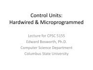
Micro–Programmed Version of the Control Unit<br />
We have just shown the signal generation trees for the hardwired version of the control unit.<br />
We now present the micro–programmed version of the same unit.<br />
We begin with a summary of the control signals used. This table is just a listing of the<br />
signals. At some time later, these signals will be assigned numeric codes and the table<br />
shown in another presentation. Note that the first row in the table is unlabeled, reflecting the<br />
fact that we must allow for no activity on each of the units.<br />
Bus 1 Bus 2 Bus 3 ALU Other<br />
PC B1 1 B2 B3 PC tra1 L / R’<br />
MAR B1 B3 MAR tra2 A<br />
R B1 R B2 B3 R shift C<br />
IR B1 MBR B2 B3 IR not READ<br />
SP B1 IOD B2 B3 SP add WRITE<br />
B3 MBR sub extend<br />
B3 IOD and 0 RUN<br />
B3 IOA or<br />
xor<br />
Microcoding (microprogramming) is another way of generating control signals. Rather than<br />
generating these signals from hardwired gates, these are generated from words in a memory<br />
unit, called a micro–memory. To illustrate this concept, consider a simple micro–controller<br />
to generate control signals for bus B1.<br />
Figure: A Sample Micro–Memory<br />
Here we see an example, written in the style of horizontal micro–coding (soon to be defined)<br />
with one bit in the micro–memory for each of the control signals to be emitted. When the<br />
word at micro–address 105 is read into the micro–MBR (the register at the bottom), the<br />
control signals generated are PC B1 = 0, MAR B1 = 1, R B1 = 0, IR B1 = 0,<br />
and SP B1 = 0. Thus, copying micro–word 105 into the Micro–MBR asserts<br />
MAR B1. Similarly, copying micro–word 106 into the Micro–MBR asserts R B1.<br />
Page 537 CPSC 5155 Last Revised July 9, 2011<br />
Copyright © 2011 by Edward L. Bosworth, Ph.D. All rights reserved.
Chapter 15 Boz–7 Implementation of the CPU<br />
Horizontal vs. Vertical Micro–Code<br />
The micro–programming strategy called “horizontal microcode” allows one bit in the<br />
micro–memory for each control signal generated. We have illustrated this with a small<br />
memory to issue control signals for bus B1. There are five control signals associated with<br />
this bus, so this part of the micro–memory would <strong>com</strong>prise five–bit numbers.<br />
A quick count from the table of control signals shows that there are thirty–four discrete<br />
control signals associated with this control unit. A full horizontal implementation of the<br />
microcode would thus require 34 bits in each micro–word just to issue the control signals.<br />
The memory width is not a big issue; indeed there are <strong>com</strong>mercial <strong>com</strong>puters with much<br />
wider micro–memories. We just note the width requirement.<br />
In vertical microcoding, each signal is assigned a numeric code that is unique for its<br />
function. Thus, each of the five signals for control of bus B1 would be assigned a numeric<br />
code. The following table illustrates the codes actually used in the design of the Boz–7.<br />
Code<br />
Signal<br />
000<br />
001 PC B1<br />
010 MAR B1<br />
011 R B1<br />
100 IR B1<br />
101 SP B1<br />
It is particularly important that a vertical microcoding scheme allow for the option that no<br />
signal is being placed on the bus. In this design we reserve the code 0 for “nothing on bus”<br />
or “ALU does nothing”, etc. The three bits in this design are placed into a 3–to–8 decoder,<br />
as shown in the figure below. Admittedly, this design is slower than the horizontal<br />
microcode in that it incurs the time penalty associated with the decoder.<br />
Figure: Sample of Vertical Microcoding<br />
In this revised example, word 105 generates MAR B1 and word 106 generates R B1.<br />
Page 538 CPSC 5155 Last Revised July 9, 2011<br />
Copyright © 2011 by Edward L. Bosworth, Ph.D. All rights reserved.
Chapter 15 Boz–7 Implementation of the CPU<br />
One advantage of encoding the control signals is the unique definition of the signal for each<br />
function. As an example, consider both the horizontal and vertical encodings for bus B1. In<br />
the five–bit horizontal encoding, we were required to have at most one 1 per micro–word.<br />
An examination of that figure will show that the micro–word “10100” would assert the two<br />
control signals PC B1 and R B1 simultaneously, causing considerable difficulties. In<br />
the vertical microcoding example, the three–bit micro–word with contents “011” causes the<br />
control signal R B1, and only that control signal, to be asserted. To be repetitive, the<br />
code “000” is reserved for not specifying any source for bus B1; in which case the contents<br />
of the bus are not specified. In such a case, the ALU cannot accept input from bus B1.<br />
The design chosen for the microcode will be based on the fact that four of the CPU units<br />
(bus B1, bus B2, bus B3, and the ALU) can each have only one “function”. For this reason,<br />
the control signals for these units will be encoded. There are seven additional control<br />
signals that could be asserted in any <strong>com</strong>bination. These signals will be represented in<br />
horizontal microcode, with one bit for each signal.<br />
Structure of the Boz–7 Microcode<br />
As indicated above, the Boz–7 microcode will be a mix of horizontal and vertical<br />
microcode. The reader will note that some of the encoded fields require 3–bit codes and<br />
some require 4–bit codes. For uniformity of notation we shall require that each field be<br />
encoded in 4 bits. The requirement that each field be encoded by a 4–bit binary number has<br />
no justification in engineering practice. Rather it is a convenience to the student, designed<br />
to remove at least one minor nuisance from the tedium of writing binary microcode and<br />
converting it to hexadecimal format. Four binary bits correspond to one hex digit.<br />
Consider the following example, taken from the <strong>com</strong>mon fetch sequence.<br />
MBR B2, tra2, B3 IR.<br />
A minimal–width encoding of this sequence of control signals would yield the following.<br />
0 000 110 100 010 000 0000 0000 0000 0000 0000.<br />
Conversion of this to hexadecimal requires regrouping the bits and then rewriting.<br />
0000 1101 0001 0000 0000 0000 0000 0000 0000 or 0x0 D100 0000<br />
The four–bit constant width coding of this sequence yields the following.<br />
0000 0000 0110 0100 0010 0000 0000 0000 0000 0000 0000<br />
This is immediately converted to 0x006 4200 0000 without shuffling any bits.<br />
Dispatching the Microcode<br />
In addition to micro–words that cause control signals to be emitted, we need micro–words to<br />
sequence the execution of the microcode. This is seen most obviously in the requirement for<br />
a dispatch based on the assembly language op–code. Let’s begin with an observation that is<br />
immediately obvious. If the microprogrammed control unit is to handle each distinct<br />
assembly language opcode differently, it must have sections of microprogram that are<br />
unique to each of the assembly language instructions.<br />
The solution to this will be a dispatch microoperation, one which invokes a section of the<br />
microprogram that is selected based on the 5–bit opcode that is currently in the Instruction<br />
Register. But what is called and how does it return?<br />
Page 539 CPSC 5155 Last Revised July 9, 2011<br />
Copyright © 2011 by Edward L. Bosworth, Ph.D. All rights reserved.
Chapter 15 Boz–7 Implementation of the CPU<br />
The description above suggests the use of a micro–subroutine, which would be the<br />
microprogramming equivalent of a subroutine in either assembly language or a higher level<br />
language. This option imposes a significant control overhead in the microprogrammed<br />
control unit, one that we elect not to take.<br />
The “where to return issue” is easily handled by noting that the action next after executing<br />
any assembly language instruction is the fetching of the next one to execute. For reasons<br />
that will soon be explained, we place the first microoperation of the <strong>com</strong>mon fetch sequence<br />
at address 0x20 in the micromemory; each execution phase ends with “go to 0x20”.<br />
The structure of the dispatch operation is best considered by examination of the control<br />
signals for the <strong>com</strong>mon fetch sequence.<br />
F, T0: PC B1, tra1, B3 MAR, READ. // MAR (PC)<br />
F, T1: PC B1, 1 B2, add, B3 PC. // PC (PC) + 1<br />
F, T2: MBR B2, tra2, B3 IR. // IR (MBR)<br />
F, T3: Do something specific to the opcode in the IR.<br />
In the hardwired control unit, the major and minor state registers would play a large part in<br />
generation of the control signals for (F, T3) and the major state register would handle the<br />
operation corresponding to “dispatch”, that is selection of what to do next. Proper handling<br />
of the dispatch in the microprogrammed control unit requires an explicit micro–opcode and<br />
a slight resequencing of the <strong>com</strong>mon fetch control signals. Here is the revised sequence.<br />
F, T0: PC B1, tra1, B3 MAR, READ. // MAR (PC)<br />
F, T1: PC B1, 1 B2, add, B3 PC. // PC (PC) + 1<br />
F, T2: MBR B2, tra2, B3 IR. // IR (MBR)<br />
Dispatch based on the assembly language opcode<br />
F, T3: Do something specific to the opcode in the IR.<br />
The next issue for our consideration in the design of the structure of the microprogram is a<br />
decision on how to select the address of the micro–instruction to be executed next after the<br />
current micro–instruction. In order to clarify the choices, let’s examine the microprogram<br />
sequence for a specific assembly language instruction and see what we conclude.<br />
The assembly language instructions that most clearly illustrate the issue at hand are the<br />
register–to–register instructions. We choose the logical AND instruction and arbitrarily<br />
assume that its microprogram segment begins at address 0x80 (a new design, to be<br />
developed soon, will change this) and see what we have. Were we to base our control<br />
sequence on the model of assembly language programming, we would write it as follows.<br />
0x20 PC B1, tra1, B3 MAR, READ. // MAR (PC)<br />
0x21 PC B1, 1 B2, add, B3 PC. // PC (PC) + 1<br />
0x22 MBR B2, tra2, B3 IR. // IR (MBR)<br />
0x23 Dispatch based on the assembly language opcode<br />
0x80 R B1, R B2, and, B3 R.<br />
0x81 Go to 0x20.<br />
Page 540 CPSC 5155 Last Revised July 9, 2011<br />
Copyright © 2011 by Edward L. Bosworth, Ph.D. All rights reserved.
Chapter 15 Boz–7 Implementation of the CPU<br />
While the above sequence corresponds to a coding model that would be perfectly acceptable<br />
at the assembly language level, it presents several significant problems at the microcode<br />
level. We begin with the observation that it requires the introduction of an explicitly<br />
managed microprogram counter in addition to the micro–memory address register.<br />
The second, and most significant, drawback to the above design is that it requires two clock<br />
pulses to execute what the hardwired control unit executed in one clock pulse. One might<br />
also note that the present design calls for using two micro–words (addresses 0x80 and 0x81)<br />
where one micro–word might do. This is a valid observation, but the cost of memory is far<br />
less significant than the “time cost” to execute the extra instruction.<br />
The design choice taken here is to encode the address of the next microinstruction in each<br />
microinstruction in the microprogram. This removes the <strong>com</strong>plexity of managing a program<br />
counter and the necessity of the time–consuming explicit branch instruction. Recasting the<br />
example above in the context of our latest decision leads to the following sequence.<br />
Address Control Signals Next address<br />
0x20 PC B1, tra1, B3 MAR, READ. 0x21<br />
0x21 PC B1, 1 B2, add, B3 PC. 0x22<br />
0x22 MBR B2, tra2, B3 IR. 0x23<br />
0x23 Dispatch based on IR 31 –IR 27 . ?? – We decide later<br />
0x80 R B1, R B2, and, B3 R. 0x20<br />
Note that the introduction of an explicit next address causes the execution phase of the<br />
logical AND instruction to be reduced to one clock pulse, as desired. The requirement for<br />
uniformity of microcode words leads to use of an explicit next address in every micro–word<br />
in the micromemory. The only microinstruction that appears not to require an explicit next<br />
address in the dispatch found at address 0x23.<br />
A possible use for the next address field of the dispatch instruction is seen when we consider<br />
the effort put into the hardwired control unit to avoid wasting execution time on a Branch<br />
instruction when the branch condition was not met. The implementation of this decision in a<br />
microprogrammed control unit is to elect not to dispatch to the opcode–specific microcode<br />
when the instruction is a branch and the condition is not met. What we have is shown<br />
below.<br />
Address Control Signals Next address<br />
0x20 PC B1, tra1, B3 MAR, READ. 0x21<br />
0x21 PC B1, 1 B2, add, B3 PC. 0x22<br />
0x22 MBR B2, tra2, B3 IR. 0x23<br />
0x23 Dispatch based on IR 31 –IR 27 . 0x20<br />
0x80 R B1, R B2, and, B3 R. 0x20<br />
The present design places the next address for dispatch when the condition is not met in the<br />
field of the micro–word associated with the next address for two reasons:<br />
1. This results in a more regular design, one that is faster and easier to implement.<br />
2. This avoids “hard coding” the address of the beginning of the <strong>com</strong>mon fetch.<br />
Page 541 CPSC 5155 Last Revised July 9, 2011<br />
Copyright © 2011 by Edward L. Bosworth, Ph.D. All rights reserved.
Chapter 15 Boz–7 Implementation of the CPU<br />
At this point in the design of the microprogrammed control unit, we have two distinct types<br />
of microoperations: a type that issues control signals and a type that dispatches based on the<br />
assembly language opcode. To handle this distinction, we introduce the idea of a micro–<br />
opcode with the following values at present.<br />
Micro–Op Function<br />
0000 Issue control signals<br />
0001 Dispatch based on the assembly language opcode.<br />
We have stated that there are conditions under which the dispatch will not be taken. There<br />
is only one condition that will not be dispatched: the assembly–language opcode is 0x0F and<br />
the branch condition is not met. Before we consider how to handle this situation, we must<br />
first address another design issue, that presented by indirect addressing.<br />
Handling Defer<br />
Consider the control signals for the LDR (Load Register) assembly language instruction.<br />
LDR Op-Code = 01100<br />
(Hexadecimal 0x0C)<br />
F, T0: PC B1, tra1, B3 MAR, READ. // MAR (PC)<br />
F, T1: PC B1, 1 B2, add, B3 PC. // PC (PC) + 1<br />
F, T2: MBR B2, tra2, B3 IR. // IR (MBR)<br />
F, T3: IR B1, R B2, add, B3 MAR. // Do the indexing.<br />
Here the major state register takes control.<br />
1) If the I–bit (bit 26) is 1, then the Defer state is entered.<br />
2) If the I–bit is 0, then the E state is entered.<br />
D, T0: READ. // Address is already in the MAR.<br />
D, T1: WAIT. // Cannot access the MBR just now.<br />
D, T2: MBR B2, tra2, B3 MAR. // MAR (MBR)<br />
D, T3: WAIT.<br />
Here the transition is automatic from the D state to the E state.<br />
E, T0: READ. // Again, address is already in the MAR.<br />
E, T1: WAIT.<br />
E, T2: MBR B2, tra2, B3 R.<br />
E, T3: WAIT.<br />
The issue here is that we no longer have an explicit major state register to handle the<br />
sequencing of major states. The microprogram itself must handle the sequencing; it must do<br />
something different for each of the two possibilities: indirect addressing is used and indirect<br />
addressing is not used. Assuming a dispatch to address 0x0C for LDR (as it will be done in<br />
the final design), the current design calls for the following microinstruction at that address.<br />
Address Control Signals Next address<br />
0x0C IR B1, R B2, add, B3 MAR. Depends on IR 26 .<br />
Suddenly we need two “next addresses”, one if the defer phase is to be entered and one to be<br />
used if that phase is not to be entered. This last observation determines the final form of the<br />
microprogram; each micro–word has length 44 bits with structure as shown below.<br />
Page 542 CPSC 5155 Last Revised July 9, 2011<br />
Copyright © 2011 by Edward L. Bosworth, Ph.D. All rights reserved.
Chapter 15 Boz–7 Implementation of the CPU<br />
In this representation of the microprogram words, we use “D = 0” to indicate that the defer<br />
phase is not to be entered and “D = 1” to indicate that it should be entered. This notation<br />
will be made more precise after we explore the new set of signals used to control the<br />
sequencing of the microprogram. Here we assume no more than 256 micro–words in the<br />
control store.<br />
Micro–Op B1 B2 B3 ALU M1 M2 D = 0 D = 1<br />
4 bit 4 bit 4 bit 4 bit 4 bit 4 bit 4 bit 8 bit 8 bit<br />
Notes:<br />
1. The width of each field is either four or eight bits. The main reason for this is<br />
to facilitate the use of hexadecimal notation in writing the microcode.<br />
2. The use of four bits to encode only two options for the micro–opcode may appear<br />
extravagant. This follows our desire for a very regular structure.<br />
3. The use of “D = 0” and “D = 1” is not exactly appropriate for the dispatch<br />
instruction with micro–opcode = 0001. We shall explain this later.<br />
4. The bits associated with the M1 field are those specifying the shift parameters<br />
Bit 3 L / R (1 for a left shift, 0 for a right shift)<br />
Bit 2 A (1 for an arithmetic shift)<br />
Bit 1 C (1 for circular shift)<br />
Bit 0<br />
Not used<br />
5. The bits associated with the M2 field are<br />
Bit 3 READ (Indicates a memory reference)<br />
Bit 2 WRITE (Unless READ = 1)<br />
Bit 1 extend (Sign–extend contents of IR when copying to B1)<br />
Bit 0 0 RUN (Stop the <strong>com</strong>puter)<br />
6. For almost every micro–instruction, the two “next addresses” are identical. For<br />
these, we cannot predict the value of the generated control signal “branch” and do<br />
not care, since the next address will be independent of that value.<br />
7. The values for next addresses will each be two hexadecimal digits. It is here that<br />
we have made the explicit assumption on the maximum size of the micromemory.<br />
Sequencing the Boz–7 Microprogrammed Control Unit<br />
In addition to the assembly language opcode, we shall need two new signals in order to<br />
sequence the microprogrammed control unit correctly. We call these two control signals<br />
“S1” and “S2”, because they resemble the control signals S 1 and S 2 used in the hardwired<br />
control unit but are not exactly identical.<br />
In the hardwired control unit, the signal S 1 was used to determine whether or not the state<br />
following Fetch would again be Fetch. This allowed <strong>com</strong>pletion of the execution of 14 of<br />
the 22 assembly language instructions in the Fetch phase. In the microprogrammed control<br />
unit, the signal S1 will be used to determine whether or not the dispatch microinstruction is<br />
executed. The only condition under which it is not executed is that in which the assembly<br />
language calls for a conditional branch and the branch condition is not met.<br />
Page 543 CPSC 5155 Last Revised July 9, 2011<br />
Copyright © 2011 by Edward L. Bosworth, Ph.D. All rights reserved.
Chapter 15 Boz–7 Implementation of the CPU<br />
This leads to a simple statement defining this sequencing signal.<br />
S1 = 0 if and only if the assembly language opcode = 0x0F and branch = 0,<br />
where branch = 1 if and only if the branch condition is met.<br />
The sequencing signal S2 is used to control the entering of the defer code for those<br />
instructions that can use indirect addressing. Recall that the assignment of opcodes to the<br />
assembly language instructions has been structured so that only instructions beginning with<br />
“011” can enter the defer phase. Even these enter the defer phase only when IR 26 = 1.<br />
Thus, we have the following definition of this signal.<br />
S2 = 1 if and only if (IR 31 = 0, IR 30 = 1, IR 29 = 1, and IR 26 = 1)<br />
In a way, this is exactly the definition of the sequencing control signal S 2 as used in the<br />
hardwired control unit. The only difference is that in this design the signal S2 must be used<br />
independently of the signal S1, so we must use the full definition. The figure below<br />
illustrates the circuitry to generate the two sequencing signals S1 and S2.<br />
Given these circuits, we have the final form and labeling of the micro–words in the micro–<br />
memory. Note that there are no “micro–data” words, only microinstructions.<br />
Micro–Op B1 B2 B3 ALU M1 M2 S2 = 0 S2 = 1<br />
4 bit 4 bit 4 bit 4 bit 4 bit 4 bit 4 bit 8 bit 8 bit<br />
The form of the type 1 instruction is <strong>com</strong>pletely defined and can be given as follows.<br />
Micro–Op B1 B2 B3 ALU M1 M2 D = 0 D = 1<br />
0001 0x0 0x0 0x0 0x0 0x0 0x0 0x20 0x20<br />
But what exactly does this dispatch instruction do? The question be<strong>com</strong>es one of defining<br />
the dispatch table, which is used to determine the address of the microcode that is invoked<br />
explicitly by this dispatch. We now address that issue.<br />
Page 544 CPSC 5155 Last Revised July 9, 2011<br />
Copyright © 2011 by Edward L. Bosworth, Ph.D. All rights reserved.
Chapter 15 Boz–7 Implementation of the CPU<br />
The design of the Boz–7 uses a dispatch mechanism copied from that used by Andrew S.<br />
Tanenbaum in his textbook Structured Computer Organization [R15]. It is apparent that this<br />
dispatch mechanism is <strong>com</strong>monly used in many <strong>com</strong>mercial implementations of microcode.<br />
The solution is to use the opcode itself as the dispatch address. As the Boz–7 uses a five bit<br />
opcode, the sequencer unit for the microprogrammed control unit must expand it to an 8–bit<br />
address by adding three high order 0 bits so that the dispatch address is 000 ¢ IR31–27. As<br />
an example, the binary opcode for LDR is 01100; its dispatch address is 0000 1100 or 0x0C.<br />
The Boz–7 uses five–bit opcodes, with range 0x00 through 0x1F. It then follows that<br />
addresses 0x00 through 0x1F in the micromemory must be reserved for dispatch addresses.<br />
It is for this reason that the <strong>com</strong>mon fetch sequence begins at address 0x20; that is the next<br />
available address. We now see that this structure works only because the address of the<br />
next microinstruction is explicitly encoded in the microinstruction.<br />
This dispatch mechanism works very well on the 14 of 22 assembly language instructions<br />
that <strong>com</strong>plete execution in one additional clock pulse. As examples, we examine the control<br />
signals for the first 8 opcodes (0x00 – 0x07) along with the <strong>com</strong>mon fetch microcode.<br />
Address Micro Control Signals Next Address<br />
Opcode S2 = 0 S2 = 1<br />
0x00 0 0 RUN 0x20 0x20<br />
0x01 0 IR B1, extend, tra1, B3 R 0x20 0x20<br />
0x02 0 IR B1, R B2, and, B3 R 0x20 0x20<br />
0x03 0 IR B1, R B2, extend, add, B3 R 0x20 0x20<br />
0x04 0 NOP 0x20 0x20<br />
0x05 0 NOP 0x20 0x20<br />
0x06 0 NOP 0x20 0x20<br />
0x07 0 NOP 0x20 0x20<br />
0x20 0 PC B1, tra1, B3 MAR, READ 0x21 0x21<br />
0x21 0 PC B1, 1 B2, add, B3 PC 0x22 0x22<br />
0x22 0 MBR B2, tra2, B3 IR 0x23 0x23<br />
0x23 1 Dispatch based on opcode 0x20 0x20<br />
At this point, our design continues to look sound. Note that the unused opcodes (those at<br />
microprogram addresses 0x04 through 0x07) simply do nothing and return to the <strong>com</strong>mon<br />
fetch sequence at address 0x20. This allows for future expansion of the instruction set.<br />
The only problem left to be addressed is the proper handling of instructions that require<br />
more than one clock cycle (following the <strong>com</strong>mon fetch) in which to execute. The first such<br />
instruction is the GET assembly language instruction.<br />
Page 545 CPSC 5155 Last Revised July 9, 2011<br />
Copyright © 2011 by Edward L. Bosworth, Ph.D. All rights reserved.
Chapter 15 Boz–7 Implementation of the CPU<br />
The control signals for the GET assembly language instruction, as implemented in the<br />
hardwired control unit are shown below. Note that (F, T3) here does nothing as the<br />
instruction cannot be <strong>com</strong>pleted in Fetch and I decided not to make the (F, T3) signal<br />
generation tree more <strong>com</strong>plex when I could force the execution into (E, T0) and (E, T2).<br />
GET Op-Code = 01000 (Hexadecimal 0x08)<br />
F, T0: PC B1, tra1, B3 MAR, READ. // MAR (PC)<br />
F, T1: PC B1, 1 B2, add, B3 PC. // PC (PC) + 1<br />
F, T2: MBR B2, tra2, B3 IR. // IR (MBR)<br />
F, T3: NOP.<br />
E, T0: IR B1, tra1, B3 IOA. // Send out the I/O address<br />
E, T1: WAIT.<br />
E, T2: IOD B2, tra2, B3 R. // Get the results.<br />
E, T3: NOP.<br />
Noting that the NOP microoperations in this sequence are used only because there is nothing<br />
that can be done during those clock pulses, we can rewrite the sequence as follows.<br />
GET Op-Code = 01000 (Hexadecimal 0x08)<br />
T0: PC B1, tra1, B3 MAR, READ. // MAR (PC)<br />
T1: PC B1, 1 B2, add, B3 PC. // PC (PC) + 1<br />
T2: MBR B2, tra2, B3 IR. // IR (MBR)<br />
T3: IR B1, tra1, B3 IOA. // Send out the I/O address<br />
T4: IOD B2, tra2, B3 R. // Get the results.<br />
This fits into the structure of the microcode fairly well, except that it seems to call for two<br />
instructions to be placed at address 0x08. The solution to the problem is based on the fact<br />
that each microinstruction must encode the address of the next microinstruction. Just select<br />
the next available word in micromemory and place the “rest of the execution sequence”<br />
there. What we have is as follows.<br />
Address Micro Control Signals Next Address<br />
Opcode S2 = 0 S2 = 1<br />
0x08 0 IR B1, tra1, B3 IOA. 0x24 0x24<br />
0x20 0 PC B1, tra1, B3 MAR, READ 0x21 0x21<br />
0x21 0 PC B1, 1 B2, add, B3 PC 0x22 0x22<br />
0x22 0 MBR B2, tra2, B3 IR 0x23 0x23<br />
0x23 1 Dispatch based on opcode 0x20 0x20<br />
0x24 0 IOD B2, tra2, B3 R. 0x20 0x20<br />
In software engineering, such a structure is called “spaghetti code” and is highly<br />
discouraged. The reason is simple; one writes a few thousand lines in this style and nobody<br />
(including the original author) can follow the logic. The microprogram, however, <strong>com</strong>prises<br />
a small number (fewer than 33) independent threads of short (less than 12) instructions. For<br />
such a structure, even spaghetti code can be tolerated.<br />
Page 546 CPSC 5155 Last Revised July 9, 2011<br />
Copyright © 2011 by Edward L. Bosworth, Ph.D. All rights reserved.
Chapter 15 Boz–7 Implementation of the CPU<br />
Assignment of Numeric Codes to Control Signals<br />
We now start writing the microcode. This step begins with the assignment of numeric<br />
values to the control signals that the control unit emits.<br />
The next table shows the numeric codes that this author has elected to assign to the encoded<br />
control signals; these being the controls for bus B1, bus B2, bus B3, and the ALU. While<br />
the assignment may appear almost random, it does have some logic. The basic rule is that<br />
code 0 does nothing. The bus codes have been adjusted to have the greatest <strong>com</strong>monality;<br />
thus code 6 is the code for both MBR B2 and B3 MBR.<br />
Code Bus 1 Bus 2 Bus 3 ALU<br />
0<br />
1 PC B1 1 B2 B3 PC tra1<br />
2 MAR B1 B3 MAR tra2<br />
3 R B1 R B2 B3 R shift<br />
4 IR B1 B3 IR not<br />
5 SP B1 B3 SP add<br />
6 MBR B2 B3 MBR sub<br />
7 IOD B2 B3 IOD and<br />
8 B3 IOA or<br />
9 xor<br />
10<br />
Other assignments may be legitimately defended, but this is the one we use. There is no<br />
assignment for Code = 2 on Bus 2. This is the result of a recent revision. The control signal<br />
for Code = 2 was deleted, but your author did not want to change the other codes.<br />
Example: Common Fetch Sequence<br />
We begin our discussion of microprogramming by listing the control signals for the first<br />
three minor cycles in the Fetch major cycle and translating these to microcode. We shall<br />
mention here, and frequently, that the major and minor cycles are present in the microcode<br />
only implicitly. It is better to think that major cycles map into sections of microcode.<br />
For this example, we do the work explicitly.<br />
Location 0x20 F, T0: PC B1 B1 code is 1<br />
tra1 ALU code is 1<br />
B3 MAR B3 code is 2<br />
READ M2(Bit 3) = 1, so M2 = 8<br />
Micro–Op = 0. B2 code and M1 code are both 0.<br />
Address Micro-Op B1 B2 B3 ALU M1 M2 S2 = 0 S2 = 1<br />
0x20 0 1 0 2 1 0 8 0x21 0x21<br />
Page 547 CPSC 5155 Last Revised July 9, 2011<br />
Copyright © 2011 by Edward L. Bosworth, Ph.D. All rights reserved.
Chapter 15 Boz–7 Implementation of the CPU<br />
Location 0x21 F, T1: PC B1 B1 code is 1<br />
1 B2 B2 code is 1<br />
add ALU code is 5<br />
B3 PC. B3 code is 1<br />
Address Micro-Op B1 B2 B3 ALU M1 M2 S2 = 0 S2 = 1<br />
0x21 0 1 1 1 5 0 0 0x22 0x22<br />
Location 0x22 F, T2: MBR B2 B2 code is 6<br />
tra2 ALU code is 2<br />
B3 IR B3 code is 4<br />
Address Micro-Op B1 B2 B3 ALU M1 M2 S2 = 0 S2 = 1<br />
0x22 0 0 6 4 2 0 0 0x23 0x23<br />
Location 0x23<br />
Dispatch on the op–code in the machine language instruction<br />
For this we assume that the Micro–Op is 1 and that none of the other fields are used.<br />
Address Micro-Op B1 B2 B3 ALU M1 M2 S2 = 0 S2 = 1<br />
0x23 1 0 0 0 0 0 0 0x20 0x20<br />
Here is the microprogram for the <strong>com</strong>mon fetch sequence.<br />
Address Micro-Op B1 B2 B3 ALU M1 M2 S2 = 0 S2 = 1<br />
0x20 0 1 0 2 1 0 8 0x21 0x21<br />
0x21 0 1 1 1 5 0 0 0x22 0x22<br />
0x22 0 0 6 4 2 0 0 0x23 0x23<br />
0x23 1 0 0 0 0 0 0 0x20 0x20<br />
Here is the section of microprogram for the <strong>com</strong>mon fetch sequence, written in the form that<br />
would be seen in a utility used for debugging the microcode.<br />
Address Contents<br />
0x20 0x010 2108 2121<br />
0x21 0x011 1500 2222<br />
0x22 0x006 4200 2323<br />
0x23 0x100 0000 2020<br />
We now have assembled all of the design tricks required to write microcode and have<br />
examined some microcode in detail. It is time to finish the microprogramming.<br />
Page 548 CPSC 5155 Last Revised July 9, 2011<br />
Copyright © 2011 by Edward L. Bosworth, Ph.D. All rights reserved.
Chapter 15 Boz–7 Implementation of the CPU<br />
The Execution of Op–Codes 0x00 through 0x07<br />
The first four of these machine instructions (0x00 –0x00) use immediate addressing and<br />
execute in a single cycle, while the last four (0x04 –0x07) are NOP’s, also executing in a<br />
single cycle. The microcode for these goes in addresses 0x00 through 0x07 of the<br />
micro–memory. The next step for each of these is Fetch for the next instruction, so the next<br />
address for all of them is 0x20.<br />
HLT Op-Code = 00000 0 RUN.<br />
Address Micro-Op B1 B2 B3 ALU M1 M2 S2 = 0 S2 = 1<br />
0x00 0 0 0 0 0 0 1 0x20 0x20<br />
LDI Op-Code = 00001 IR B1, extend, tra1, B3 R.<br />
Address Micro-Op B1 B2 B3 ALU M1 M2 S2 = 0 S2 = 1<br />
0x01 0 4 0 3 1 0 2 0x20 0x20<br />
ANDI Op-Code = 00010 IR B1, R B2, and, B3 R.<br />
Address Micro-Op B1 B2 B3 ALU M1 M2 S2 = 0 S2 = 1<br />
0x02 0 4 3 3 7 0 0 0x20 0x20<br />
ADDI Op-Code = 00011 IR B1, R B2, extend, add, B3 R.<br />
Address Micro-Op B1 B2 B3 ALU M1 M2 S2 = 0 S2 = 1<br />
0x03 0 1 3 3 5 0 2 0x20 0x20<br />
We are now in a position to specify the first eight micro–words.<br />
Address Micro-Op B1 B2 B3 ALU M1 M2 S2 = 0 S2 = 1<br />
0x00 0 0 0 0 0 0 1 0x20 0x20<br />
0x01 0 4 0 3 1 0 2 0x20 0x20<br />
0x02 0 4 3 3 7 0 0 0x20 0x20<br />
0x03 0 1 3 3 5 0 2 0x20 0x20<br />
0x04 0 0 0 0 0 0 0 0x20 0x20<br />
0x05 0 0 0 0 0 0 0 0x20 0x20<br />
0x06 0 0 0 0 0 0 0 0x20 0x20<br />
0x07 0 0 0 0 0 0 0 0x20 0x20<br />
Based on the tables above, we state the contents of the first eight micro–words.<br />
Address Contents<br />
0x00 0x 000 0001 2020<br />
0x01 0x 040 3102 2020<br />
0x02 0x 043 3700 2020<br />
0x03 0x 013 3502 2020<br />
0x04 0x 000 0000 2020<br />
0x05 0x 000 0000 2020<br />
0x06 0x 000 0000 2020<br />
0x07 0x 000 0000 2020<br />
Page 549 CPSC 5155 Last Revised July 9, 2011<br />
Copyright © 2011 by Edward L. Bosworth, Ph.D. All rights reserved.
Chapter 15 Boz–7 Implementation of the CPU<br />
For the moment, let’s skip the next eight opcodes and finish the simpler cases.<br />
LLS Op-Code = 10000 R B2, shift, L / R = 1, A = 0. C = 0, B3 R.<br />
Address Micro-Op B1 B2 B3 ALU M1 M2 S2 = 0 S2 = 1<br />
0x10 0 0 3 3 3 8 0 0x20 0x20<br />
LCS Op-Code = 10001 R B2, shift, L / R = 1, A = 0. C = 1, B3 R.<br />
Address Micro-Op B1 B2 B3 ALU M1 M2 S2 = 0 S2 = 1<br />
0x11 0 0 3 3 3 9 0 0x20 0x20<br />
RLS Op-Code = 10010 R B2, shift, L / R = 0, A = 0. C = 0, B3 R.<br />
Address Micro-Op B1 B2 B3 ALU M1 M2 S2 = 0 S2 = 1<br />
0x12 0 0 3 3 3 0 0 0x20 0x20<br />
RAS Op-Code = 10011 R B2, shift, L / R = 0, A = 1. C = 0, B3 R.<br />
Address Micro-Op B1 B2 B3 ALU M1 M2 S2 = 0 S2 = 1<br />
0x13 0 0 3 3 3 4 0 0x20 0x20<br />
NOT Op-Code = 10100 R B2, not, B3 R.<br />
Address Micro-Op B1 B2 B3 ALU M1 M2 S2 = 0 S2 = 1<br />
0x14 0 0 3 3 4 0 0 0x20 0x20<br />
ADD Op-Code = 10101 R B1, R B2, add, B3 R.<br />
Address Micro-Op B1 B2 B3 ALU M1 M2 S2 = 0 S2 = 1<br />
0x15 0 3 3 3 5 0 0 0x20 0x20<br />
SUB Op-Code = 10110 R B1, R B2, sub, B3 R.<br />
Address Micro-Op B1 B2 B3 ALU M1 M2 S2 = 0 S2 = 1<br />
0x16 0 3 3 3 6 0 0 0x20 0x20<br />
AND Op-Code = 10111 R B1, R B2, and, B3 R.<br />
Address Micro-Op B1 B2 B3 ALU M1 M2 S2 = 0 S2 = 1<br />
0x17 0 3 3 3 7 0 0 0x20 0x20<br />
OR Op-Code = 11000 R B1, R B2, or, B3 R.<br />
Address Micro-Op B1 B2 B3 ALU M1 M2 S2 = 0 S2 = 1<br />
0x18 0 3 3 3 8 0 0 0x20 0x20<br />
XOR Op-Code = 11001 R B1, R B2, xor, B3 R.<br />
Address Micro-Op B1 B2 B3 ALU M1 M2 S2 = 0 S2 = 1<br />
0x19 0 3 3 3 9 0 0 0x20 0x20<br />
We have now <strong>com</strong>pleted the microprogramming for all but eight of the instructions. The<br />
table on the next page shows what we have generated up to this point.<br />
Page 550 CPSC 5155 Last Revised July 9, 2011<br />
Copyright © 2011 by Edward L. Bosworth, Ph.D. All rights reserved.
Chapter 15 Boz–7 Implementation of the CPU<br />
Address Micro-Op B1 B2 B3 ALU M1 M2 S2 = 0 S2 = 1<br />
0x00 0 0 0 0 0 0 1 0x20 0x20<br />
0x01 0 4 0 3 1 0 2 0x20 0x20<br />
0x02 0 4 3 3 7 0 0 0x20 0x20<br />
0x03 0 1 3 3 5 0 2 0x20 0x20<br />
0x04 0 0 0 0 0 0 0 0x20 0x20<br />
0x05 0 0 0 0 0 0 0 0x20 0x20<br />
0x06 0 0 0 0 0 0 0 0x20 0x20<br />
0x07 0 0 0 0 0 0 0 0x20 0x20<br />
0x08<br />
0x09<br />
0x0A<br />
0x0B<br />
0x0C<br />
0x0D<br />
0x0E<br />
0x0F<br />
0x10 0 0 3 3 3 8 0 0x20 0x20<br />
0x11 0 0 3 3 3 9 0 0x20 0x20<br />
0x12 0 0 3 3 3 0 0 0x20 0x20<br />
0x13 0 0 3 3 3 4 0 0x20 0x20<br />
0x14 0 0 3 3 4 0 0 0x20 0x20<br />
0x15 0 3 3 3 5 0 0 0x20 0x20<br />
0x16 0 3 3 3 6 0 0 0x20 0x20<br />
0x17 0 3 3 3 7 0 0 0x20 0x20<br />
0x18 0 3 3 3 8 0 0 0x20 0x20<br />
0x19 0 3 3 3 9 0 0 0x20 0x20<br />
0x1A 0 0 0 0 0 0 0 0x20 0x20<br />
0x1B 0 0 0 0 0 0 0 0x20 0x20<br />
0x1C 0 0 0 0 0 0 0 0x20 0x20<br />
0x1D 0 0 0 0 0 0 0 0x20 0x20<br />
0x1E 0 0 0 0 0 0 0 0x20 0x20<br />
0x1F 0 0 0 0 0 0 0 0x20 0x20<br />
0x20 0 1 0 2 1 0 8 0x21 0x21<br />
0x21 0 1 1 1 5 0 0 0x22 0x22<br />
0x22 0 0 6 4 2 0 0 0x23 0x23<br />
0x23 1 0 0 0 0 0 0 0x20 0x20<br />
Note that instructions 0x1A through 0x1F are not yet implemented, so they show as NOP’s.<br />
We now move to those instructions that require Defer and Execute for <strong>com</strong>pletion. Due to<br />
the ordering of the op–codes, we first investigate those instructions that cannot enter Defer.<br />
Page 551 CPSC 5155 Last Revised July 9, 2011<br />
Copyright © 2011 by Edward L. Bosworth, Ph.D. All rights reserved.
Chapter 15 Boz–7 Implementation of the CPU<br />
GET Op-Code = 01000 (Hexadecimal 0x08)<br />
F, T3: WAIT.<br />
E, T0: IR B1, tra1, B3 IOA. // Send out the I/O address<br />
E, T1: WAIT.<br />
E, T2: IOD B2, tra2, B3 R. // Get the results.<br />
E, T3: WAIT.<br />
As noted above, we can ignore any WAIT signal that is not required by considerations of<br />
memory timing. The first of two microoperations is associated with the dispatch address for<br />
the GET instruction and the second one at the first available micromemory word.<br />
IR B1, tra1, B3 IOA.<br />
Address Micro-Op B1 B2 B3 ALU M1 M2 S2 = 0 S2 = 1<br />
0x08 0 4 0 8 1 0 0 0x24 0x24<br />
IOD B2, tra2, B3 R.<br />
Address Micro-Op B1 B2 B3 ALU M1 M2 S2 = 0 S2 = 1<br />
0x24 0 0 7 7 2 0 0 0x20 0x20<br />
PUT Op-Code = 01001 (Hexadecimal 0x09)<br />
F, T3: WAIT.<br />
E, T0: R B2, tra2, B3 IOD // Get the data ready<br />
E, T1: WAIT.<br />
E, T2: IR B1, tra1, B3 IOA. // Sending out the address<br />
E, T3: WAIT. // causes the output of data.<br />
R B2, tra2, B3 IOD<br />
Address Micro-Op B1 B2 B3 ALU M1 M2 S2 = 0 S2 = 1<br />
0x09 0 0 3 7 2 0 0 0x25 0x25<br />
IR B1, tra1, B3 IOA.<br />
Address Micro-Op B1 B2 B3 ALU M1 M2 S2 = 0 S2 = 1<br />
0x25 0 4 0 8 1 0 0 0x20 0x20<br />
RET Op-Code = 01010<br />
(Hexadecimal 0x0A)<br />
F, T3: WAIT<br />
E, T0: SP B1, + 1 B2, add, B3 SP. // Increment the SP<br />
E, T1: SP B1, tra1, B3 MAR, READ. // Get the return address<br />
E, T2: WAIT.<br />
E, T3: MBR B2, tra2, B3 PC. // Put return address into PC<br />
Here we have three non–waiting instructions plus a WAIT that is necessary for the memory<br />
access. As a result, we must allocate four micro–memory words to the execution.<br />
Page 552 CPSC 5155 Last Revised July 9, 2011<br />
Copyright © 2011 by Edward L. Bosworth, Ph.D. All rights reserved.
Chapter 15 Boz–7 Implementation of the CPU<br />
SP B1, + 1 B2, add, B3 SP<br />
Address Micro-Op B1 B2 B3 ALU M1 M2 S2 = 0 S2 = 1<br />
0x0A 0 5 1 5 5 0 0 0x26 0x26<br />
SP B1, tra1, B3 MAR, READ.<br />
Address Micro-Op B1 B2 B3 ALU M1 M2 S2 = 0 S2 = 1<br />
0x26 0 5 0 2 1 0 8 0x27 0x27<br />
WAIT<br />
Address Micro-Op B1 B2 B3 ALU M1 M2 S2 = 0 S2 = 1<br />
0x27 0 0 0 0 0 0 0 0x28 0x28<br />
MBR B2, tra2, B3 PC<br />
Address Micro-Op B1 B2 B3 ALU M1 M2 S2 = 0 S2 = 1<br />
0x28 0 0 6 1 2 0 0 0x20 0x20<br />
RTI Op-Code = 01011 (Hexadecimal 0x0B)<br />
Not yet implemented.<br />
This is encoded as another NOP, until time to develop the details of interrupt handling.<br />
The “link”<br />
Address Micro-Op B1 B2 B3 ALU M1 M2 B = 0 B = 1<br />
0x0B 0 0 0 0 0 0 0 0x20 0x20<br />
We now turn to the four instructions that use both Defer and Execute. One might be<br />
tempted to write a <strong>com</strong>mon Defer “subroutine” to be “called” by each of the Execute<br />
sections. While this would reduce duplication of micro–code, we opt for in–line coding.<br />
In each of the following four instructions, the step corresponding to (F, T3) issues control<br />
signals. These will be issued by the “link” micro–operation. We must also introduce a new<br />
micro–op to account for conditionally entering or not entering the Defer section.<br />
Page 553 CPSC 5155 Last Revised July 9, 2011<br />
Copyright © 2011 by Edward L. Bosworth, Ph.D. All rights reserved.
Chapter 15 Boz–7 Implementation of the CPU<br />
The next four assembly language instructions (LDR, STR, JSR, and BR) are the only that<br />
possibly use indirect addressing. As discussed in our presentation of the sequencing control<br />
signals for the microprogram, the defer phase will be entered if and only if S2 = 1. The<br />
template for the DEFER state is shown below. It has one essential WAIT state.<br />
X READ<br />
X + 1 WAIT<br />
X + 2 MBR B2, tra2, B3 MAR<br />
X + 3 Code for E, T0<br />
Due to this structure, the address for (S2 = = 0) will be 3 more than that for (S2 = = 1).<br />
LDR Op-Code = 01100<br />
(Hexadecimal 0x0C)<br />
F, T3: IR B1, R B2, add, B3 MAR. // Do the indexing.<br />
D, T0: READ. // Address is already in the<br />
MAR.<br />
D, T1: WAIT. // Cannot access the MBR just now.<br />
D, T2: MBR B2, tra2, B3 MAR. // MAR (MBR)<br />
D, T3: WAIT.<br />
E, T0: READ. // Again, address is already in the MAR.<br />
E, T1: WAIT.<br />
E, T2; MBR B2, tra2, B3 R.<br />
E, T3: WAIT.<br />
IR B1, R B2, add, B3 MAR<br />
Address Micro-Op B1 B2 B3 ALU M1 M2 S2 = 0 S2 = 1<br />
0x0C 0 4 3 2 5 0 0 0x2C 0x29<br />
READ<br />
Address Micro-Op B1 B2 B3 ALU M1 M2 S2 = 0 S2 = 1<br />
0x29 0 0 0 0 0 0 8 0x2A 0x2A<br />
WAIT<br />
Address Micro-Op B1 B2 B3 ALU M1 M2 S2 = 0 S2 = 1<br />
0x2A 0 0 0 0 0 0 0 0x2B 0x2B<br />
MBR B2, tra2, B3 MAR<br />
Address Micro-Op B1 B2 B3 ALU M1 M2 S2 = 0 S2 = 1<br />
0x2B 0 0 6 2 2 0 0 0x2C 0x2C<br />
READ.<br />
Address Micro-Op B1 B2 B3 ALU M1 M2 S2 = 0 S2 = 1<br />
0x2C 0 0 0 0 0 0 8 0x2D 0x2D<br />
WAIT.<br />
Address Micro-Op B1 B2 B3 ALU M1 M2 S2 = 0 S2 = 1<br />
0x2D 0 0 0 0 0 0 0 0x2E 0x2E<br />
MBR B2, tra2, B3 MAR<br />
Address Micro-Op B1 B2 B3 ALU M1 M2 S2 = 0 S2 = 1<br />
0x2E 0 0 6 2 2 0 0 0x20 0x20<br />
Page 554 CPSC 5155 Last Revised July 9, 2011<br />
Copyright © 2011 by Edward L. Bosworth, Ph.D. All rights reserved.
Chapter 15 Boz–7 Implementation of the CPU<br />
STR Op-Code = 01101 (Hexadecimal 0x0D)<br />
F, T3: IR B1, R B2, add, B3 MAR. // Do the indexing.<br />
D, T0: READ. // Address is already in the MAR.<br />
D, T1: WAIT. // Cannot access the MBR just now.<br />
D, T2: MBR B2, tra2, B3 MAR. // MAR (MBR)<br />
D, T3: WAIT.<br />
E, T0: WAIT.<br />
E, T1; R B1, tra1, B3 MBR, WRITE.<br />
E, T2: WAIT.<br />
E, T3: WAIT.<br />
IR B1, R B2, add, B3 MAR<br />
Address Micro-Op B1 B2 B3 ALU M1 M2 S2 = 0 S2 = 1<br />
0x0D 0 4 3 2 5 0 0 0x32 0x2F<br />
READ<br />
Address Micro-Op B1 B2 B3 ALU M1 M2 S2 = 0 S2 = 1<br />
0x2F 0 0 0 0 0 0 8 0x30 0x30<br />
WAIT<br />
Address Micro-Op B1 B2 B3 ALU M1 M2 S2 = 0 S2 = 1<br />
0x30 0 0 0 0 0 0 0 0x31 0x31<br />
MBR B2, tra2, B3 MAR<br />
Address Micro-Op B1 B2 B3 ALU M1 M2 S2 = 0 S2 = 1<br />
0x31 0 0 6 2 2 0 0 0x32 0x32<br />
R B1, tra1, B3 MBR, WRITE<br />
Address Micro-Op B1 B2 B3 ALU M1 M2 S2 = 0 S2 = 1<br />
0x32 0 3 0 6 1 0 4 0x33 0x33<br />
WAIT<br />
Address Micro-Op B1 B2 B3 ALU M1 M2 S2 = 0 S2 = 1<br />
0x33 0 0 0 0 0 0 0 0x20 0x20<br />
Note here that we must have a WAIT state following the last WRITE of the execute phase.<br />
This allows the memory to <strong>com</strong>plete the instruction before the next instruction is fetched.<br />
Page 555 CPSC 5155 Last Revised July 9, 2011<br />
Copyright © 2011 by Edward L. Bosworth, Ph.D. All rights reserved.
Chapter 15 Boz–7 Implementation of the CPU<br />
JSR Op-Code = 01110 (Hexadecimal 0x0E)<br />
F, T3: IR B1, R B2, add, B3 MAR. // Do the indexing.<br />
D, T0: READ. // Address is already in the MAR.<br />
D, T1: WAIT. // Cannot access the MBR just now.<br />
D, T2: MBR B2, tra2, B3 MAR. // MAR (MBR)<br />
D, T3: WAIT.<br />
E, T0: PC B1, tra1, B3 MBR. // Put return address in MBR<br />
E, T1: MAR B1, tra1, B3 PC. // Set up for jump to target.<br />
E, T2: SP B1, tra1, B3 MAR, WRITE. // Put return address on stack.<br />
E, T3: SP B1, 1 B2, sub, B3 SP. // Bump SP<br />
IR B1, R B2, add, B3 MAR<br />
Address Micro-Op B1 B2 B3 ALU M1 M2 S2 = 0 S2 = 1<br />
0x0E 0 4 3 2 5 0 0 0x37 0x34<br />
READ<br />
Address Micro-Op B1 B2 B3 ALU M1 M2 S2 = 0 S2 = 1<br />
0x34 0 0 0 0 0 0 8 0x35 0x35<br />
WAIT<br />
Address Micro-Op B1 B2 B3 ALU M1 M2 S2 = 0 S2 = 1<br />
0x35 0 0 0 0 0 0 0 0x36 0x36<br />
MBR B2, tra2, B3 MAR<br />
Address Micro-Op B1 B2 B3 ALU M1 M2 S2 = 0 S2 = 1<br />
0x36 0 0 6 2 2 0 0 0x37 0x37<br />
PC B1, tra1, B3 MBR<br />
Address Micro-Op B1 B2 B3 ALU M1 M2 S2 = 0 S2 = 1<br />
0x37 0 1 0 6 1 0 0 0x38 0x38<br />
MAR B1, tra1, B3 PC<br />
Address Micro-Op B1 B2 B3 ALU M1 M2 S2 = 0 S2 = 1<br />
0x38 0 2 0 1 1 0 0 0x39 0x39<br />
SP B1, tra1, B3 MAR, WRITE<br />
Address Micro-Op B1 B2 B3 ALU M1 M2 S2 = 0 S2 = 1<br />
0x39 0 5 0 2 1 0 0 0x3A 0x3A<br />
SP B1, 1 B2, sub, B3 SP<br />
Address Micro-Op B1 B2 B3 ALU M1 M2 S2 = 0 S2 = 1<br />
0x3A 0 5 1 5 6 0 0 0x20 0x20<br />
Page 556 CPSC 5155 Last Revised July 9, 2011<br />
Copyright © 2011 by Edward L. Bosworth, Ph.D. All rights reserved.
Chapter 15 Boz–7 Implementation of the CPU<br />
BR Op-Code = 01111 (Hexadecimal 0x0F)<br />
F, T3: IR B1, R B2, add, B3 MAR. // Do the indexing.<br />
D, T0: READ. // Address is already in the MAR.<br />
D, T1: WAIT. // Cannot access the MBR just now.<br />
D, T2: MBR B2, tra2, B3 MAR. // MAR (MBR)<br />
D, T3: WAIT.<br />
E, T0: WAIT.<br />
E, T1: WAIT.<br />
E, T2: WAIT.<br />
E, T3: MAR B1, tra1, B3 PC.<br />
Remember that the microcode at address 0x23 will not dispatch to address 0x0F if the<br />
branch condition is not true. This avoids wasted time and incorrect execution.<br />
IR B1, R B2, add, B3 MAR<br />
Address Micro-Op B1 B2 B3 ALU M1 M2 S2 = 0 S2 = 1<br />
0x0F 0 4 3 2 5 0 0 0x3E 0x3B<br />
READ<br />
Address Micro-Op B1 B2 B3 ALU M1 M2 S2 = 0 S2 = 1<br />
0x3B 0 0 0 0 0 0 8 0x3C 0x3C<br />
WAIT<br />
Address Micro-Op B1 B2 B3 ALU M1 M2 S2 = 0 S2 = 1<br />
0x3C 0 0 0 0 0 0 0 0x3D 0x3D<br />
MBR B2, tra2, B3 MAR<br />
Address Micro-Op B1 B2 B3 ALU M1 M2 S2 = 0 S2 = 1<br />
0x3D 0 0 6 2 2 0 0 0x3E 0x3E<br />
MAR B1, tra1, B3 PC<br />
Address Micro-Op B1 B2 B3 ALU M1 M2 S2 = 0 S2 = 1<br />
0x3E 0 2 0 1 1 0 0 0x20 0x20<br />
This <strong>com</strong>pletes the derivation of the microprogram for the Boz–7.<br />
Page 557 CPSC 5155 Last Revised July 9, 2011<br />
Copyright © 2011 by Edward L. Bosworth, Ph.D. All rights reserved.
Chapter 15 Boz–7 Implementation of the CPU<br />
Here now is the <strong>com</strong>plete microprogram of the Boz–7, shown in two pages of tables.<br />
Address Micro-Op B1 B2 B3 ALU M1 M2 S2 = 0 S2 = 1<br />
0x00 0 0 0 0 0 0 1 0x20 0x20<br />
0x01 0 4 0 3 1 0 2 0x20 0x20<br />
0x02 0 4 3 3 7 0 0 0x20 0x20<br />
0x03 0 1 3 3 5 0 2 0x20 0x20<br />
0x04 0 0 0 0 0 0 0 0x20 0x20<br />
0x05 0 0 0 0 0 0 0 0x20 0x20<br />
0x06 0 0 0 0 0 0 0 0x20 0x20<br />
0x07 0 0 0 0 0 0 0 0x20 0x20<br />
0x08 0 4 0 8 1 0 0 0x24 0x24<br />
0x09 0 0 3 7 2 0 0 0x25 0x25<br />
0x0A 0 5 1 5 5 0 0 0x26 0x26<br />
0x0B 0 0 0 0 0 0 0 0x20 0x20<br />
0x0C 0 4 3 2 5 0 0 0x2C 0x29<br />
0x0D 0 4 3 2 5 0 0 0x32 0x2F<br />
0x0E 0 4 3 2 5 0 0 0x37 0x34<br />
0x0F 0 4 3 2 5 0 0 0x3E 0x3B<br />
0x10 0 0 3 3 3 8 0 0x20 0x20<br />
0x11 0 0 3 3 3 9 0 0x20 0x20<br />
0x12 0 0 3 3 3 0 0 0x20 0x20<br />
0x13 0 0 3 3 3 4 0 0x20 0x20<br />
0x14 0 0 3 3 4 0 0 0x20 0x20<br />
0x15 0 3 3 3 5 0 0 0x20 0x20<br />
0x16 0 3 3 3 6 0 0 0x20 0x20<br />
0x17 0 3 3 3 7 0 0 0x20 0x20<br />
0x18 0 3 3 3 8 0 0 0x20 0x20<br />
0x19 0 3 3 3 9 0 0 0x20 0x20<br />
0x1A 0 0 0 0 0 0 0 0x20 0x20<br />
0x1B 0 0 0 0 0 0 0 0x20 0x20<br />
0x1C 0 0 0 0 0 0 0 0x20 0x20<br />
0x1D 0 0 0 0 0 0 0 0x20 0x20<br />
0x1E 0 0 0 0 0 0 0 0x20 0x20<br />
0x1F 0 0 0 0 0 0 0 0x20 0x20<br />
0x20 0 1 0 2 1 0 8 0x21 0x21<br />
0x21 0 1 1 1 5 0 0 0x22 0x22<br />
0x22 0 0 6 4 2 0 0 0x23 0x23<br />
0x23 1 0 0 0 0 0 0 0x00 0x00<br />
Page 558 CPSC 5155 Last Revised July 9, 2011<br />
Copyright © 2011 by Edward L. Bosworth, Ph.D. All rights reserved.
Chapter 15 Boz–7 Implementation of the CPU<br />
Address Micro-Op B1 B2 B3 ALU M1 M2 S2 = 0 S2 = 1<br />
0x24 0 0 7 7 2 0 0 0x20 0x20<br />
0x25 0 4 0 8 1 0 0 0x20 0x20<br />
0x26 0 5 0 2 1 0 8 0x27 0x27<br />
0x27 0 0 0 0 0 0 0 0x28 0x28<br />
0x28 0 0 6 1 2 0 0 0x20 0x20<br />
0x29 0 0 0 0 0 0 8 0x2A 0x2A<br />
0x2A 0 0 0 0 0 0 0 0x2B 0x2B<br />
0x2B 0 0 6 2 2 0 0 0x2C 0x2C<br />
0x2C 0 0 0 0 0 0 8 0x2D 0x2D<br />
0x2D 0 0 0 0 0 0 0 0x2E 0x2E<br />
0x2E 0 0 6 2 2 0 0 0x20 0x20<br />
0x2F 0 0 0 0 0 0 8 0x30 0x30<br />
0x30 0 0 0 0 0 0 0 0x31 0x31<br />
0x31 0 0 6 2 2 0 0 0x32 0x32<br />
0x32 0 3 0 6 1 0 4 0x33 0x33<br />
0x33 0 0 0 0 0 0 0 0x20 0x20<br />
0x34 0 0 0 0 0 0 8 0x35 0x35<br />
0x35 0 0 0 0 0 0 0 0x36 0x36<br />
0x36 0 0 6 2 2 0 0 0x37 0x37<br />
0x37 0 1 0 6 1 0 0 0x38 0x38<br />
0x38 0 2 0 1 1 0 0 0x39 0x39<br />
0x39 0 5 0 2 1 0 0 0x3A 0x3A<br />
0x3A 0 5 1 5 6 0 0 0x20 0x20<br />
0x3B 0 0 0 0 0 0 8 0x3C 0x3C<br />
0x3C 0 0 0 0 0 0 0 0x3D 0x3D<br />
0x3D 0 0 6 2 2 0 0 0x3E 0x3E<br />
0x3E 0 2 0 1 1 0 0 0x20 0x20<br />
The last address is 0x3E = 62 (in decimal). The microprogram has used 63 of the available<br />
256 addresses (it is an 8–bit address) for a 25% usage. With 63 addresses used, we could<br />
have opted for a 6–bit address. We chose an 8–bit address for the sake of simplicity.<br />
The reader will note that this leaves plenty of unused microprogram space for possible<br />
implementation of any new instructions.<br />
Page 559 CPSC 5155 Last Revised July 9, 2011<br />
Copyright © 2011 by Edward L. Bosworth, Ph.D. All rights reserved.
Chapter 15 Boz–7 Implementation of the CPU<br />
The Sequencer for the Microprogrammed Control Unit<br />
We now discuss the micro–control unit, which is responsible for sequencing the control unit<br />
itself, which is microprogrammed.<br />
Recall that there are no “microdata” in the microprogram, but only microinstructions. Based<br />
on this observation, the only function of the micro–control unit is the selection of the next<br />
address to place into the micro–memory address register (MAR).<br />
There are four sources for this address.<br />
1. the assembly language opcode,<br />
2. the S2 = 0 field of the microinstruction,<br />
3. the S2 = 1 field of the microinstruction, and<br />
4. a constant register 0x20 which is used only when the <strong>com</strong>puter is started.<br />
Here is the circuit for the micro–control unit, omitting only the constant register.<br />
Page 560 CPSC 5155 Last Revised July 9, 2011<br />
Copyright © 2011 by Edward L. Bosworth, Ph.D. All rights reserved.
Chapter 15 Boz–7 Implementation of the CPU<br />
Summary of Control Signals<br />
This is a summary of control signals, organized by bus and functional unit. It is designed to<br />
support discussions of microprogramming, but can stand on its own as a handy table.<br />
Code Bus 1 Bus 2 Bus 3 ALU<br />
0<br />
1 PC B1 1 B2 B3 PC tra1<br />
2 MAR B1 B3 MAR tra2<br />
3 R B1 R B2 B3 R shift<br />
4 IR B1 B3 IR not<br />
5 SP B1 B3 SP add<br />
6 MBR B2 B3 MBR sub<br />
7 IOD B2 B3 IOD and<br />
8 B3 IOA or<br />
9 xor<br />
10<br />
Miscellaneous control signals Specified by the M1 and M2 fields<br />
These fields are not encoded, so that each bit can be set separately. Each of M1 and M2 is a<br />
four bit field, having bits Bit 3 , Bit 2 , Bit 1 , and Bit 0 .<br />
Bit Number Shift Select Other Signals<br />
Bit 3 L / R READ<br />
Bit 2 A WRITE<br />
Bit 1 C extend<br />
Bit 0<br />
0 RUN<br />
Micro-Code Format<br />
The following assumes no more than 256 micro-words in the control store.<br />
On Off Next Address if<br />
Micro-Op B1 B2 B3 ALU M1 M2 Branch = 0 Branch = 1<br />
4 bit 4 bit 4 bit 4 bit 4 bit 4 bit 4 bit 8 bit 8 bit<br />
Four–bit field format<br />
Bit 3 Bit 2 Bit 1 Bit 0<br />
Page 561 CPSC 5155 Last Revised July 9, 2011<br />
Copyright © 2011 by Edward L. Bosworth, Ph.D. All rights reserved.