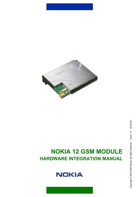
Nokia 12 GSM Module Hardware Integration ... - KORE Telematics
Nokia 12 GSM Module Hardware Integration ... - KORE Telematics
Nokia 12 GSM Module Hardware Integration ... - KORE Telematics

You also want an ePaper? Increase the reach of your titles
YUMPU automatically turns print PDFs into web optimized ePapers that Google loves.
NOKIA <strong>12</strong> <strong>GSM</strong> MODULEHARDWARE INTEGRATION MANUALCopyright © 2003-2004 <strong>Nokia</strong>. All rights reserved. Issue 1.3 923<strong>12</strong>30
ContentsACRONYMS AND TERMS ......................................................................................................11. ABOUT THIS DOCUMENT ................................................................................................32. INTRODUCTION ................................................................................................................43. MECHANICAL INTEGRATION...........................................................................................53.1 DIMENSIONS ...............................................................................................................54. ELECTRICAL INTEGRATION ............................................................................................74.1 M2M SYSTEM CONNECTOR......................................................................................74.1.1 Electrical characteristics ........................................................................................84.1.2 Connector pin-out ..................................................................................................94.2 GROUNDING .............................................................................................................164.3 POWER SUPPLY .......................................................................................................164.4 SERIAL COMMUNICATION.......................................................................................174.4.1 PORT1.................................................................................................................174.4.2 PORT2.................................................................................................................184.4.3 PORT3.................................................................................................................184.5 SIM INTERFACE ........................................................................................................184.6 AUDIO INTERFACE ...................................................................................................194.6.1 Analog audio........................................................................................................194.6.1.1 Analog audio example ..................................................................................214.6.1.2 Acoustic echo ...............................................................................................234.6.2 Digital audio .........................................................................................................234.6.2.1 Sign-extended linear code ............................................................................245. RF AND ANTENNA INTEGRATION.................................................................................265.1 ANTENNA INSTALLATION ........................................................................................266. TEST BOARD FOR THE NOKIA <strong>12</strong> <strong>GSM</strong> MODULE .......................................................286.1 POWERING................................................................................................................286.2 SIM CARD READER ..................................................................................................286.3 RS-232 CONVERTERS..............................................................................................286.4 AUDIO ........................................................................................................................297. CERTIFICATIONS............................................................................................................32
7.1.1 RX-2.....................................................................................................................327.1.2 RX-9.....................................................................................................................327.2 TECHNICAL REQUIREMENTS .................................................................................337.2.1 SIM testing...........................................................................................................337.2.2 Power supply .......................................................................................................337.2.3 EMC/ESD and safety tests ..................................................................................337.2.4 RF testing ............................................................................................................337.2.5 RF exposure ........................................................................................................347.2.6 Additional type approval notes.............................................................................34REFERENCES.......................................................................................................................35APPENDIX: NOKIA <strong>12</strong> TEST BOARD PART LIST, ASSEMBLY DRAWING ANDSCHEMATICS ..................................................................................................................36
Legal NoticeCopyright © 2003-2004 <strong>Nokia</strong>. All rights reserved.Reproduction, transfer, distribution or storage of part or all of the contents in this document in any form without theprior written permission of <strong>Nokia</strong> is prohibited.<strong>Nokia</strong> and <strong>Nokia</strong> Connecting People are registered trademarks of <strong>Nokia</strong> Corporation. Java and all Java-basedmarks are trademarks or registered trademarks of Sun Microsystems, Inc. Other product and company namesmentioned herein may be trademarks or trade names of their respective owners.<strong>Nokia</strong> operates a policy of continuous development. <strong>Nokia</strong> reserves the right to make changes and improvementsto any of the products described in this document without prior notice.Under no circumstances shall <strong>Nokia</strong> be responsible for any loss of data or income or any special, incidental,consequential or indirect damages howsoever caused.The contents of this document are provided "as is". Except as required by applicable law, no warranties of anykind, either express or implied, including, but not limited to, the implied warranties of merchantability and fitnessfor a particular purpose, are made in relation to the accuracy, reliability or contents of this document. <strong>Nokia</strong>reserves the right to revise this document or withdraw it at any time without prior notice.RX-9:FCC/INDUSTRY CANADA NOTICEYour device may cause TV or radio interference (for example, when using a telephone in close proximity toreceiving equipment). The FCC or Industry Canada can require you to stop using your telephone if suchinterference cannot be eliminated. If you require assistance, contact your local service facility. This devicecomplies with part 15 of the FCC rules. Operation is subject to the condition that this device does not causeharmful interference.
ACRONYMS AND TERMSAcronym/termAACA/DAPIATDescriptionAmpere°C CelciusCECORBACMOSCSDCTSdBdBiDCDCDDCEDSRDTEDTREARNEARPEDGEE<strong>GSM</strong>EMCESDFAlternating CurrentAnalog-to-DigitalApplication Programming InterfaceATtention (command language)Mark for a product that fulfils the EU safety andR&TTE requirementsCommon Object Request Broker ArchitectureComplementary Metal-Oxide SemiconductorCircuit Switched DataClear To SendDecibelAntenna GainDirect CurrentData Carrier DetectData Circuit Terminating EquipmentData Set ReadyData Terminal EquipmentData Terminal ReadyEarphone Amplifier Inverting Input PinEarphone Amplifier Non-Inverting Input PinEnhanced Data Rates for Global EvolutionExtended <strong>GSM</strong>Electromagnetic CompatibilityElectrostatic DischargeFarad°F FahrenheitFCCGGSNGPRSFederal Communications CommissionGateway GPRS Support NodeGeneral Packet Radio Service1/44
Acronym/termGPS<strong>GSM</strong>HBMHi-ZHSCSDHWHzICIPM2MMICNMICPMMCXPCBPCMRFRIRS-232RTSRX-2RX-9SIMSMSSWTCPUARTUDPVWDescriptionGlobal Positioning SystemGlobal System for Mobile CommunicationHuman Body ModelHigh ImpedanceHigh Speed Circuit Switched Data<strong>Hardware</strong>HertzIntegrated CircuitInternet ProtocolMachine-to-machineMicrophone amplifier inverting input pinMicrophone amplifier non-inverting input pinMiniature MicroaxPrinted Circuit BoardPulse Code ModulationRadio FrequencyRing IndicatorInterface, standardised by the Electronic IndustriesAlliance (EIA), for communication betweencomputers, terminals, and modemsRequest to SendType designation for the <strong>Nokia</strong> <strong>12</strong> <strong>GSM</strong> module(E<strong>GSM</strong> 900/<strong>GSM</strong> 1800 MHz bands)Type designation for the <strong>Nokia</strong> <strong>12</strong> <strong>GSM</strong> module(<strong>GSM</strong> 850/<strong>GSM</strong> 1900 MHZ bands)Subscriber Identity <strong>Module</strong>Short Message ServiceSoftwareTransmission Control ProtocolUniversal Asynchronous Receiver/TransmitterUser Datagram ProtocolVoltWatt2/44
1. ABOUT THIS DOCUMENTThis document provides instructions for the <strong>Nokia</strong> <strong>12</strong> <strong>GSM</strong> module (hereafter<strong>Nokia</strong> <strong>12</strong> module) hardware integration. The document is intended to help thesystem integrator to integrate the <strong>Nokia</strong> <strong>12</strong> module into a remote end hardwareapplication and to gain the necessary type approvals.The document describes the mechanical, electrical and radio frequency (RF)integration as well as antenna installation. In addition the document describesthe technical characteristics of the <strong>Nokia</strong> <strong>12</strong> test board, and lists thecertifications and technical requirements needed for type approval.Note: For more information on the <strong>Nokia</strong> <strong>12</strong> module usage and softwareintegration, see the <strong>Nokia</strong> <strong>12</strong> <strong>GSM</strong> <strong>Module</strong> Product Specification, <strong>Nokia</strong> M2MPlatform Software Developer’s Guide and <strong>Nokia</strong> M2M Platform <strong>Nokia</strong> <strong>12</strong> <strong>GSM</strong><strong>Module</strong> IMlet Programming Guide.3/44
2. INTRODUCTIONThe <strong>Nokia</strong> <strong>12</strong> module has been designed for M2M (machine-to-machine)applications and other wireless solutions. There are two versions of the <strong>Nokia</strong><strong>12</strong> module:• RX-2 dual-band <strong>GSM</strong> device supporting EDGE, GPRS, HSCSD, CSD, andSMS in E<strong>GSM</strong> 900/<strong>GSM</strong> 1800 MHz bands• RX-9 dual band <strong>GSM</strong> device supporting EDGE, GPRS, CSD, SMS in <strong>GSM</strong>850/<strong>GSM</strong> 1900 MHZ bands.The <strong>Nokia</strong> <strong>12</strong> module can be used in several applications due to its threedifferent operating modes. Simple I/O applications can be easily implementedby using the <strong>Nokia</strong> <strong>12</strong> module in the User control mode that offers messagepersonalising, secure messaging, and timing functionality for SMS controlledI/O applications. In the AT command mode, the <strong>Nokia</strong> <strong>12</strong> module can be usedas a <strong>GSM</strong> modem. In modem use, all supported bearers are available. The<strong>Nokia</strong> <strong>12</strong> module is <strong>Nokia</strong> M2M Platform compatible. In the M2M system mode,the <strong>Nokia</strong> <strong>12</strong> module communicates with the server application through the<strong>Nokia</strong> M2M Gateway, and all the compatible features of the <strong>Nokia</strong> <strong>12</strong> moduleare available for developing a wide range of M2M applications.In addition to the different operating modes, the <strong>Nokia</strong> <strong>12</strong> module has anintegrated TCP/IP stack which enables direct GPRS or <strong>GSM</strong> data connectionbetween a remote end application and a server application. Due to theintegrated TCP/IP stack, the HTTP and Socket APIs of the <strong>Nokia</strong> <strong>12</strong> areavailable for application development.In addition to the bearers and operating modes listed above, the <strong>Nokia</strong> <strong>12</strong>supports several Java APIs, location service for external GPS moduleintegration, reliability features like AutoPIN, <strong>GSM</strong> encryption and securitycodes, reset mechanism and <strong>Nokia</strong> M2M Platform authentication. Javatechnology support enables upgrading the application software over-the-air,and smart messaging makes the installation flexible. <strong>GSM</strong> phase 2+supplementary services enable voice application development.Note: All data bearers as well as TCP/IP are dependent on network support.4/44
3. MECHANICAL INTEGRATIONThe <strong>Nokia</strong> <strong>12</strong> module contains two holes for mounting screws. The screws canbe used in mounting, but are not compulsory. The <strong>Nokia</strong> <strong>12</strong> module has beentested according to the automotive standard DIN 72300-3 (although not invarious temperatures), and it can be integrated into various applications withoutthe screws.3.1 DIMENSIONSThe general dimensions and overall area of the <strong>Nokia</strong> <strong>12</strong> module are listed inTable 1 and Table 2.Table 1. General dimensions of the <strong>Nokia</strong> <strong>12</strong> <strong>GSM</strong> module (in millimetresand inches)Height 36 mm 1.41 inchWidth 45 mm 1.77 inchThickness 9 mm 0.35 inchTable 2. Overall area of the <strong>Nokia</strong> <strong>12</strong> <strong>GSM</strong> module (in square centimetresand square inches)Area 16.2 cm 2 2.48 inch 2The detailed physical dimensions (in millimeters) of the <strong>Nokia</strong> <strong>12</strong> module areshown in Figure 1.5/44
Figure 1. Detailed physical dimensions of the <strong>Nokia</strong> <strong>12</strong> <strong>GSM</strong> module (inmillimetres)6/44
4. ELECTRICAL INTEGRATION4.1 M2M SYSTEM CONNECTORAll signals are routed through the M2M System Connector, except the antenna,which is routed through the miniature microax (MMCX) RF connector.The M2M System Connector is a 60-pin (2 rows, 30 pins per row), 1.27mm/0.05 inch pitch pin header connector. It has a frame that helps in thephysical integration and also holds the <strong>Nokia</strong> <strong>12</strong> module firmly in position.The possible mating connector is described in Table 3.Table 3. Possible mating connectors for the <strong>Nokia</strong> <strong>12</strong> moduleSupplier Part number DescriptionSAMTEC SFMC-130-02-S-D Female connector. Board-to-boardSAMTEC SFM-130-02-S-D Female connector. Board-to-board.With alignment mark.Table 4 defines the recommended operating conditions for the actual deviceand/or interface operation, and Table 5 defines the absolute maximum ratings.Table 4. Recommended operating conditionsParameter Value NoteSupply Voltage (V BB ) 3.6…4.0 V (3.8 V typical) Voltage must neverdrop below the lowlimit.Logic voltage (I/Ovoltage)DC output source or sinkcurrent (any I/O pin, useradjustable)Operating temperaturerange1.8…5.0 V0…5 V Upper limitdepending on I/Ovoltage.-10…+55 °C+14…+131 °FTable 5. Absolute maximum ratingsParameterSupply voltageDC input voltage (any signal pin)Value+4.2 V-0.5…5.5 V7/44
ParameterValueOperating temperature range -25…+55 °C-13…+131 °FStorage temperature range -40…+85 °C-40…+185 °F4.1.1 Electrical characteristicsAll digital outputs (1-9) are open drain outputs, and all pins have a 10 kohmpull-up resistor to I/O voltage.Table 6. Digital output characteristicsParameterApplication load resistanceApplication load capacitanceHigh level output voltage minimum (Io=-20µA)Low level output voltage maximum (Io=1mA)Value>100 kohm
Table 8. Digital input characteristicsParameterApplication driving impedanceLow level input voltage (IO VOLTAGE/pin 521.8 - 5V)High level input voltage ((IO VOLTAGE/pin 521.8 - 5V)Value
Figure 2. Pin numbering of the <strong>Nokia</strong> <strong>12</strong> M2M System ConnectorThe pin-out of the M2M System Connector in shown in Table 11.Table 11. M2M System Connector pin-outPin Name Pin Name1 VBB 2 GND3 VBB 4 GND5 VBB 6 GND7 VBB 8 GND9 VBB 10 GND11 NC <strong>12</strong> NC13 NC 14 NC15 MICP 16 EARP17 MICN 18 EARN19 AD3 20 AD221 PCMDCLK 22 PCMSCLK23 PCMTX 24 PCMRX25 RESET T 26 RESET A27 PORT1RX 28 NC29 PORT1TX 30 OUTPUT231 OUTPUT3 32 OUTPUT410/44
Pin Name Pin Name33 OUTPUT5 34 INPUT635 INPUT5 36 AD137 BSI 38 PORT2RX39 PORT2TX 40 PORT2RTS41 PORT2CTS 42 OUTPUT843 INPUT8 44 OUTPUT945 SLEEPX 46 INPUT1147 VSIM 48 SIMRST49 SIMCLK 50 SIMDATA51 SIMDET 52 IO VOLTAGE53 OUTPUT1/P3RX 54 INPUT4/P3TX55 INPUT10 56 INPUT757 OUTPUT6 58 OUTPUT759 INPUT9 60 NCThe pin functions are described in Table <strong>12</strong>.Table <strong>12</strong>. M2M System Connector pin descriptionsPin Name Description1 VBB Device power. Voltage nominal 3.8 V, 3.6 V – 4.0 V,maximum current 2A peak. Regulated power input forthe <strong>Nokia</strong> <strong>12</strong> module.All V BB pins must be connected together at theapplication end. The device end is not fuse-protected,so the application should provide sufficient overloadprotection.Current consumption can be as high as 2 A whentransmitting at full power. When the <strong>Nokia</strong> <strong>12</strong> moduleis transmitting data, there is a current peak (max. 2A )at 4.6 ms intervals that lasts 0.577ms (1 TX slot) or1.154 ms (2 TX slots). Average power consumption isabout 500 mA. The power supply should be designedaccording to this.If the operating voltage falls below 3.4 V, the <strong>Nokia</strong><strong>12</strong> module automatically shuts down. For moreinformation on the power supply, see Chapter 4.3.2 GND Return ground for device power. These pins are usedfor device power (V BB ) return ground. Connect tocommon ground. All GND pins must be connected at11/44
Pin Name Description3 VBB See PIN 14 GND See PIN 25 VBB See PIN 16 GND See PIN 27 VBB See PIN 18 GND See PIN 29 VBB See PIN 110 GND See PIN 211 NC Not used<strong>12</strong> NC Not used13 NC Not used14 NC Not usedthe application end. For more information ongrounding, see Chapter 4.2.15 MICP MICP is used with analog audio as differentialpositive input. The line is AC coupled at the deviceend. Frequency response is 300 - 3400 Hz. For moreinformation on the analog audio, see chapter 4.6.1.16 EARP EARP is used with analog audio as differentialpositive output. Frequency response is 300 - 3400Hz. For more information on the analog audio, seeChapter 4.6.1.17 MICN MICN is used with analog audio as differentialnegative input. The line is AC coupled at the deviceend. Frequency response is 300 - 3400 Hz. For moreinformation on the analog audio, see chapter 4.6.1.18 EARN EARN is used with analog audio as differentialnegative output. Frequency response is 300 - 3400Hz. For more information on the analog audio, seechapter 4.6.1.19 AD3 Input for 10 bit analog-to-digital (A/D) converter. Theapplication end must scale voltage level between 0 -2.8 V.20 AD2 See PIN 1921 PCMDCLK PCMDCLK is a 5<strong>12</strong> kHz digital audio clock from theapplication module. Logic level is set by the IOVOLTAGE pin (pin 52). For more information on thedigital audio, see Chapter 4.6.2.22 PCMSCLK PCMSCLK is one PCMDCLK cycle that repeats itselfevery 64 PCMDCLK cycles. Frame sync frequency isthus is 8 kHz. The logic level is set by the IO<strong>12</strong>/44
Pin Name DescriptionVOLTAGE pin (pin 52). For more information on thedigital audio, see Chapter 4.6.2.23 PCMTX Digital audio, transmits data from the device to theapplication. Logic level is set by the IO VOLTAGE pin(pin 52). For more information on the digital audio,see Chapter 4.6.2.24 PCMRX Digital audio, receives data from the application to thedevice. Logic level is set by the IO VOLTAGE pin (pin52). For more information on the digital audio, seeChapter 4.6.2.25 RESET T Reset input for the <strong>Nokia</strong> <strong>12</strong> module, active low. The<strong>Nokia</strong> <strong>12</strong> module is reset when this line is low. Logiclevel is set by the IO VOLTAGE pin (pin 52).Minimum duration is approximately 500 ms.26 RESET A Reset output for the application, active low. Resetgoes high after approximately 170 ms of power-up.Logic level is set by the IO VOLTAGE pin (pin 52).27 PORT1RX PORT1 receive. PORT1RX is an asynchronous serialchannel receive pin. Functionality otherwise as in pin29, PORT1TX. Logic level is set by the IO VOLTAGEpin (pin 52).28 NC Not used29 PORT1TX PORT1 transmit. PORT1TX is an asynchronousserial channel transmit pin that can be used with pin27 (PORT1RX) to form a full duplex serial link. Pins30-35 can be used to provide handshaking functions.Logic level is set by the IO VOLTAGE pin (pin52)30 OUTPUT2 Digital output from device. Logic level is set by the IOVOLTAGE pin (pin 52). If the AT command mode isactive, this pin is used as a Data Carrier Detect(DCD) output for Port 1.31 OUTPUT3 Digital output from module. Logic level is set by theIO VOLTAGE pin (pin 52). If the AT command modeis active, this pin is used as Data Set Ready (DSR)output for Port 1.32 OUTPUT4 Digital output from module. Logic level is set by theI/O voltage pin (pin 52). If the AT command mode isactive, this pin is used as Clear To Send (CTS) outputfor Port 1.33 OUTPUT5 Digital output from module. Logic level is set by theIO VOLTAGE pin (pin 52). If the AT command modeis active, this pin is used as Ring Indicator (RI) outputfor Port 1.34 INPUT6 Digital input to module. Logic level is set by the IOVOLTAGE pin (pin 52). If the AT command mode isactive, this pin is used as Request To Send (RTS)13/44
Pin Name Descriptioninput for Port 1.35 INPUT5 Digital input to module. Logic level is set by the IOVOLTAGE pin (pin 52). If the AT command mode isactive, this pin is used as Data Terminal Ready (DTR)input for Port 136 AD1 Input for 10 bit A/D converter. The application endmust scale voltage level between 0 to 2.8 V.37 BSI Input for 10 bit A/D converter. The application endmust scale voltage level between 0 to 2.8 V.38 PORT2RX PORT2 receive. PORT2RX is an asynchronous serialchannel receive pin and it is used with pin 39. Logiclevel is set by the IO VOLTAGE pin (pin 52).39 PORT2TX PORT2 Transmit. PORT2RX is an asynchronousserial channel transmit pin that is used with pin 38.Logic level is set by the IO VOLTAGE pin (pin 52).40 PORT2RTS RTS for PORT2. PORT2RTS provides handshakingsignal for asynchronous communication between the<strong>Nokia</strong> <strong>12</strong> module and the application when usingPORT2. Works together with pin 41. Logic level is setby the IO VOLTAGE pin (pin 52).41 PORT2CTS CTS for PORT2. PORT2CTS provides handshakingsignal for asynchronous communication between the<strong>Nokia</strong> <strong>12</strong> module and the application when usingPORT2. Works together with pin 40. Logic level is setby the IO VOLTAGE pin (pin 52).42 OUTPUT8 Digital output from the <strong>Nokia</strong> <strong>12</strong> module. Logic level isset by the IO VOLTAGE pin (pin 52).43 INPUT8 Digital input to the <strong>Nokia</strong> <strong>12</strong> module. Logic level is setby the IO VOLTAGE pin (pin 52).44 OUTPUT9 Digital output from the <strong>Nokia</strong> <strong>12</strong> module. Logic level isset by the IO VOLTAGE pin (pin 52).45 SLEEPX Sleep indicator of the <strong>Nokia</strong> <strong>12</strong> module. When the<strong>Nokia</strong> <strong>12</strong> module is in the sleep mode, the level ofthis output pin is low, otherwise high. The sleep modeis automatic. Logic level is set by the IO VOLTAGEpin (pin 52).46 INPUT11 Digital input to the <strong>Nokia</strong> <strong>12</strong> module. Logic level is setby the IO VOLTAGE pin (pin 52).47 VSIM Operating voltage for the SIM card, generated by the<strong>Nokia</strong> <strong>12</strong> module. For more information on the SIMinterface, see Chapter 4.5.48 SIMRST Reset signal for the SIM card, generated by the <strong>Nokia</strong><strong>12</strong> module. For more information on the SIMinterface, see Chapter 4.5.14/44
Pin Name Description49 SIMCLK Clock signal for the SIM card, generated by the <strong>Nokia</strong><strong>12</strong> module. For more information on the SIMinterface, see Chapter 4.5.50 SIMDATA Data line between the SIM card and the <strong>Nokia</strong> <strong>12</strong>module. For more information on the SIM interface,see Chapter 4.5.51 SIMDET SIM card detection signal. For more information onthe SIM interface, see Chapter 4.5.52 IO VOLTAGE This pin sets logic level for the application. Voltagemust be 1.8 V - 5.0 V. For more information on thepower supply, see Chapter 4.3.53 OUTPUT1 /PORT3RXDigital output from the <strong>Nokia</strong> <strong>12</strong> module. Logic level isset by the IO VOLTAGE pin (pin 52). If PORT3 isconfigured for serial communication, this is a receive(input) signal.54 INPUT4 /PORT3TXNote! Direction changes if pin 53 is configured forserial communication.Digital input to the <strong>Nokia</strong> <strong>12</strong> module. Logic level is setby the IO VOLTAGE pin (pin 52). If PORT3 isconfigured for serial communication, this is atransmitter (output) signal.Note! Direction changes if pin 54 is configured forserial communication.55 INPUT10 Digital input to the <strong>Nokia</strong> <strong>12</strong> module. Logic level is setby the IO VOLTAGE pin (pin 52).56 INPUT7 Digital input to the <strong>Nokia</strong> <strong>12</strong> module. Logic level is setby the IO VOLTAGE pin (pin 52).57 OUTPUT6 Digital output from the <strong>Nokia</strong> <strong>12</strong> module. Logic level isset by the IO VOLTAGE pin (pin 52).58 OUTPUT7 Digital output from the <strong>Nokia</strong> <strong>12</strong> module. Logic level isset by the IO VOLTAGE pin (pin 52).59 INPUT9 Digital input to the <strong>Nokia</strong> <strong>12</strong> module. Logic level is setby the IO VOLTAGE pin (pin 52).60 NC Not used15/44
4.2 GROUNDINGThere is only one common ground for the power supply and I/Os in the <strong>Nokia</strong><strong>12</strong> module. That is, there are no separate analog/digital ground pins in the M2MSystem Connector.All ground pins must be connected together at the application end. Groundingthrough screws is not allowed. The mounting screws must be isolated from theapplication ground.4.3 POWER SUPPLYThe <strong>Nokia</strong> <strong>12</strong> module is powered by the hardware application to which it isintegrated. The operating voltage must not fall below the specification limitunder any circumstances. The recommended operation conditions are shown inTable 4. For example, at full power, the TX can be up to 2 A, when current isdrawn from the power supply. There are no capacitors on the power supply lineof the <strong>Nokia</strong> <strong>12</strong> module, so the application must provide sufficient filtering.The power supply must be capable of supplying at least 3 W average power,but it is recommended that the power supply also provides the peak current.Otherwise a large capacitor bank is needed to compensate the voltage dropduring transmit bursts.The <strong>Nokia</strong> <strong>12</strong> module does not have protection for over-voltage of current, sothe hardware application must be equipped with one if there is a possibility forover-voltage. The hardware application should at least include a fuse.The ripple on the operating voltage must not exceed 100 mV and the voltagemust never drop below 3.6 V during operation.The application must also produce I/O voltage. The logic levels of digital inputsand outputs correspond to this I/O voltage. I/O voltage can be supplied from alinear regulator.16/44
Figure 3. Example powering with simple DC/DC converter and linearregulator4.4 SERIAL COMMUNICATIONThe <strong>Nokia</strong> <strong>12</strong> module is accessible through three different asynchronous serialinterfaces with different protocols. The pins provide one asynchronous channelwith a simple handshaking capability. The usage of the 3 ports can beconfigured with the <strong>Nokia</strong> <strong>12</strong> Configurator software. The <strong>Nokia</strong> <strong>12</strong> Configuratoris downloadable at www.forum.nokia.com/m2m free of charge.The <strong>Nokia</strong> <strong>12</strong> module supports the industry standard DB9 RS-232C connection,but an external level converter is required. For more information on theavailable handshake signals for different ports, see Chapters 4.4.1, 4.4.2 and4.4.3.The <strong>Nokia</strong> <strong>12</strong> module is a DCE (Data Communication Equipment) and thehardware application to which it is integrated is a DTE (Data TerminalEquipment). One possible method of implementing the level conversions is touse a MAX3237 transceiver or an equivalent integrated circuit (IC) levelconverter.Note: When port settings are changed, the new settings will not become validuntil the <strong>Nokia</strong> <strong>12</strong> module is restarted.4.4.1 PORT1PORT1 provides the first asynchronous channel. This port can be used with full8 signal RS-232 handshaking signals. The baud rate for PORT1 can bebetween <strong>12</strong>00 and 230400 bit/s.17/44
Note: Baud rate 230400 bit/s can be used only with AT command mode andautobauding.There are several settings for PORT1. The default setting for PORT1 is ‘HWDetection’. This means that when a 68 kohm resistor is set between the BSI(pin 37) and the ground, the <strong>Nokia</strong> <strong>12</strong> module enters the AT command modewhen it is started. It is also possible to set the AT command mode on by usingthe <strong>Nokia</strong> <strong>12</strong> Configurator (the connection type is set to ‘AT’).The <strong>Nokia</strong> <strong>12</strong> module provides all signals for the industry standard DB9 RS-232C connection, but an external level converter is required.4.4.2 PORT2PORT2 provides the second asynchronous channel with a simple handshakingcapability (only RTS and CTS). The baud rate for PORT2 can be set to 9600,19200, 38400, 57600 or 115200 bit/s. PORT2 is the default port for using theM2M System Protocol. However, if PORT1 is configured to use the M2MSystem Protocol, PORT2 cannot be used.4.4.3 PORT3PORT3 provides the third asynchronous channel with no hardwarehandshakes. The baud rate for PORT3 can be set between <strong>12</strong>00 and 115200bit/s.4.5 SIM INTERFACEAll leads from the M2M System Connector to the SIM card reader must beshorter than 15 cm/5.9 inches, because the voltage drop and increasingcapacitance will affect timing. Furthermore, it is recommended that a 100 nFbypass capacitor is placed as close as possible to the SIM reader on the VSIM(pin47) line.The leads between the M2M System Connector and the SIM card reader mustbe protected against interferences, and that is why the striplines must alwaysbe placed within the interlayers of the printed circuit board (PCB).Note: The striplines must never be placed to the overlayer of the PCB.A possible SIM card reader supplier is listed in Table 13.Table 13. Possible SIM card reader supplier18/44
The analog TX path (from the external application to the <strong>Nokia</strong> <strong>12</strong> module) hasa DC isolation inside the <strong>Nokia</strong> <strong>12</strong> module with 100 nF capacitors, and thesecapacitors together with the microphone preamplifier input impedance form a 1 storder high pass filter with 32 Hz roll-off (-3 dB).Table 14. Microphone audio characteristicsName Symbol Min Type Max UnitsDifferential inputvoltage range formicrophone input(MICP & MICN)Microphone amplifierinput resistorCommon mode voltagelevel0.316 2.0 V PPRMIC 30 50 kohmVCM 1.3 1.35 1.4 VThe earphone lines from the <strong>Nokia</strong> <strong>12</strong> module are driven differentially toachieve the best possible audio quality, free of radio frequency noise. In thedifferential mode, positive output is driven from EARP and negative signal fromEARN output.Table 15. Earphone audio characteristicsName Test condition Min Type Max UnitsOutput voltage swingin fully differentialmodeEARP to EARN 0.316 2 V PPOutput resistance 1 ohmLoad resistanceLoad resistanceLoad capacitanceCommon voltage levelfor Earphone outputEARP to EARN(with dynamictransducer)EARP to EARN(with externalaudio circuitry)EARP to EARN(with externalaudio circuitry)30 45 ohm1 kohm10 nFVCMEar 0.75 0.8 0.85 VOffset voltage -50 50 mV20/44
The following chapter gives an example of using the audio properties of the<strong>Nokia</strong> <strong>12</strong> module for voice communication purposes. The circuits presented inthe example illustrate the connection methods.There are also other possibilities for using the <strong>Nokia</strong> <strong>12</strong> audio interface. Thepresented component values are examples only; the customer can adjust theapplication-specific values to achieve the best performance for the applicationin question.4.6.1.1 Analog audio exampleAnalog TX path: Due to the small audio signal level of the electret microphone,it is recommended to use a preamplifier for the microphone before connecting itto the <strong>Nokia</strong> <strong>12</strong> module. It is strongly recommended to protect the differentialconnection against RF noise. A microphone preamplifier with 20 dB input gainis recommended for reasonable uplink audio levels.Microphone input: See Figure 5.VANAR5R4VANAC1VANAR3-C2MicPR1+R6R7VANAR2-+C3MicNFigure 5. Single-ended microphone pre-amplifierAnalog RX path: In voice applications, the <strong>Nokia</strong> <strong>12</strong> module is able to drive anearphone application without external electronics. However, it is also possibleto build a high-volume loudspeaker application by using an external poweramplifier with a high sensitivity loudspeaker. The following paragraphs showexample circuits for both cases.21/44
Earphone application: An earphone can be connected to the <strong>Nokia</strong> <strong>12</strong> modulewithout external components. In Figure 6 external components are used forEMC purposes to optimise audio quality and reliability.R1L1R2C1C2J1J2Figure 6. Earphone application circuitThe recommended earphone type is dynamic. The maximum allowed load forthis application is 32 ohm. In the example circuit, L1 is the common modechoke for the suppression of common mode disturbance in the earphone lines.J1 and J2 are surge protector gaps for ESD protection. These can be replacedwith varistor or any other state-of-the-art ESD protection component. C1 andC2 are used for RF noise filtering.R1 and R2 are used as an attenuator if the signal level from the <strong>Nokia</strong> <strong>12</strong>module is too high for the application. These resistors can be replaced withlinear potentiometers and thus get adjustable volume control for the earphoneapplication. The following component list gives example values for the circuit:• L1= 1000ohm@100MHz• C1=C2=27pF• R1=R2= Must be defined together with the sensitivity of the earphoneExternal Audio Power amplifier: External audio power must be used if thereis a need to drive low impedance load as loudspeaker. Figure 7 shows anexample connection circuit for differential audio boomer. In this application onlythe connection interface to the <strong>Nokia</strong> <strong>12</strong> module is presented. For more detailedinformation on the boomer connections and specification, see the boomermanufacturer application note.22/44
VDDC4R2Differential AudioBoomerVDDEarPEarNC1C2R1R3-+R5R4VDDR6Bypass-C3Bias+Shutdown controlFigure 7. Differential external power amplifier connectionRefer to the audio boomer manufacturer and loudspeaker application notes forinformation on maximum safe ratings for the selected components. Also keep inmind the limitation of V DD to avoid overdriving the audio boomer and thusdistorting the output signal unnecessarily.4.6.1.2 Acoustic echoBecause in a <strong>GSM</strong> voice call the uplink and downlink audios are activated atthe same time, it is recommended to use common sense when evaluating asuitable distance between the loudspeaker and the microphone. The acousticecho canceller inside the <strong>Nokia</strong> <strong>12</strong> module is tuned so that the optimum resultis achieved with 20 cm or longer distance between the microphone and thespeaker. It is also advisable to locate the microphone and the loudspeaker sothat they are pointed away from each other to achieve the best possible doubletalkperformance.4.6.2 Digital audioThere is a pulse code modulation (PCM) codec interface in the <strong>Nokia</strong> <strong>12</strong>module for digital audio support. The digital audio interface supports signextended13-bit linear code (total 16 bits are transmitted).23/44
4.6.2.1 Sign-extended linear codePCM digital audio data transmission between the <strong>Nokia</strong> <strong>12</strong> module and theapplication is handled with four signals: PCMDCLK, PCMSCLK, PCMTX, andPCMRX. The format of the data transmission is sign-extended 13-bit linearcode. A total of 16 bits are transmitted, and higher order bits must be signextended.Transmission of data commences after frame sync (PCMSCLK) riseshigh for one PCMDCLK clock cycle. After returning low, each data bit istransmitted on the falling edge of PCMDCLK.PCMDClkPCMSClkPCMTxDataPCMRxData15 14 13 <strong>12</strong> 11 10MSBSign extended15 14 13 <strong>12</strong> 11 10MSBSign extended0LSB0LSBFigure 8. Timing of clock and transmission signalsThe application must provide both the PCMDCLK and PCMSCLK. PCMDCLKfrequency is 5<strong>12</strong> kHz and PCMSCLK is repeated at 8 kHz, that is, at every 64thclock cycle. All bits but the 16 data bits following the frame sync are discarded.PCMDCLK has a typical 50 % duty-cycle; a variation of 5 % can be tolerated.For detailed timing, refer to Figure 9 and Table 16. Tcyc is the cycle time (1.953microseconds) of the 5<strong>12</strong> kHz clock. The PCMSCLK rising edge must occur atthe maximum of 8 ns after the PCMSCLK rising edge.The pulse width of the frame sync pulse should be one data clock cycle.PCMDClkTd(SCL)PCMSClkTd(PCMTxData)PCMTxDataPCMRxDataTh(PCMRxData)Tsu(PCMRxData)MSBMSBFigure 9. PCM timing diagram24/44
PCM timing characteristics are described in Table 16. The coding formatpresented in Table 16 is supported, for example, by the Motorola typeMC145483 codec.Table 16. PCM timing characteristicsParameter Symbol Min Max UnitDelay time (PCMSClk valid afterPCMDClk rising)Delay time (PCMTxData validafter PCMDClk rising)PCMRxData setup time beforePCMDClk falling edgePCMRxData hold time afterPCMDClk falling edgeTd(SClk) 0 8 nsTd(TxData) 5 25 nsTsu(RxData) 20 Tcyc-20 nsTh(RxData) 20 Tcyc-20 ns25/44
5. RF AND ANTENNA INTEGRATIONThe RF requirements for the <strong>Nokia</strong> <strong>12</strong> module are type-dependent:• RF requirements for the RX-2 type follow the ETSI E<strong>GSM</strong>900/<strong>GSM</strong>1800phase2+ specifications.• RF requirements for the RX-9 type follow the ETSI <strong>GSM</strong>850/<strong>GSM</strong>1900phase2+ specifications.Table 17. RF specifications for the <strong>Nokia</strong> <strong>12</strong> <strong>GSM</strong> moduleParameter Value DescriptionRF impedance 50 ohmRF power 2W (class 4) E<strong>GSM</strong>900 & <strong>GSM</strong> 8501W (class 1) <strong>GSM</strong>1800 & <strong>GSM</strong> 1900The RF signal from the <strong>Nokia</strong> <strong>12</strong> module to an external antenna goes troughthe MMCX connector.An adapter cable between the MMCX connector and the antenna may beneeded. Suitable connectors and cables are available, for example, fromAmphenol, TYCO, and IMS Connector Systems.The <strong>Nokia</strong> <strong>12</strong> module is certified with a Smarteq dual-band antenna (art no:1140.26 for 900/1800MHz and 1140.27 for 850/1900MHz). Suitable antennasare available, for example, from Smarteq and Hirschmann.For more information on the RF exposure, see Chapter 7.2.5.5.1 ANTENNA INSTALLATIONThe antenna must be placed within a good RF field; a location where the signalstrength is adequate. A hand-portable phone can be used to check the bestlocation for the antenna.Note: Electronic devices can cause interference, which affects the performance ofthe <strong>Nokia</strong> <strong>12</strong> module. Do not place the antenna close to electronic devices orother antennas.If an additional cable is needed between the antenna and the <strong>Nokia</strong> <strong>12</strong> module,use low-loss cables (for example RG-58. Amphenol, Suhner, etc.) andconnectors. Every additional cable, adapter, and connector increases the lossof signal power.26/44
When designing the hardware application to which the <strong>Nokia</strong> <strong>12</strong> module isintegrated into, it is important to take care of RF emissions. Do not place anysensitive components or striplines near the antenna or the antenna connector.For more information on the RF exposure, see Chapter 7.2.5.27/44
6. TEST BOARD FOR THE NOKIA <strong>12</strong> <strong>GSM</strong> MODULEThe <strong>Nokia</strong> <strong>12</strong> test board is a hardware development tool for applicationdevelopers and system integrators. It manages DC voltages, SIM card, I/O’s,and audios. You can measure several interfaces by pin headers, and thesoftware interfaces of the D9 connectors can be seen and handled. The devicecan be reset with the reset button on the test board PCB.The <strong>Nokia</strong> <strong>12</strong> module has been type approved with the <strong>Nokia</strong> <strong>12</strong> test board. Formore information on the <strong>Nokia</strong> <strong>12</strong> test board, see Appendix: <strong>Nokia</strong> <strong>12</strong> testboard part list, assembly drawing and schematics.6.1 POWERINGA 3A step down converter is used to produce module V CC . Low ESR capacitorsare used.Table 18. Powering for the <strong>Nokia</strong> <strong>12</strong> test board6.2 SIM CARD READERThe SIM card reader is directly connected to the M2M System Connector. TheVSIM (pin47) decoupling capacitor must be present in all designs. To see theconnections between the SIM card reader and the M2M System Connector, seeFigure 4.6.3 RS-232 CONVERTERSAll three serial ports of the <strong>Nokia</strong> <strong>12</strong> module are equipped with RS-232 leveltranslators and D9 connector in the test board. If they are not used, there is aswitch that can be used to set the converters in the Hi-Z mode.28/44
6.4 AUDIOFor testing analog audio, the test board includes a connector for the <strong>Nokia</strong>HSU-3 handset. The HSU-3 handset can be purchased from <strong>Nokia</strong> dealers.Figure 10. <strong>Nokia</strong> <strong>12</strong> test board microphone amplifierThe <strong>Nokia</strong> <strong>12</strong> test board and its key components are shown in Figure 11.Figure 11. <strong>Nokia</strong> <strong>12</strong> test board componentsThe <strong>Nokia</strong> <strong>12</strong> test board includes the following switches:29/44
• RS-232 translator switches for PORT1 and PORT2/PORT3−−When the RS-232 translators are on, PORT1 and PORT2/PORT3 areconnected the <strong>Nokia</strong> <strong>12</strong> module via the M2M System Connector.When the RS-232 translators are off, PORT1 and PORT2/PORT3 arenot connected the <strong>Nokia</strong> <strong>12</strong> module via the M2M System Connector.When the RS-232 translators are off, it is possible to establish aconnection to the <strong>Nokia</strong> <strong>12</strong> module by using the pin headers (1-4).• Microphone input selection switches−−MIC FROM HSU-3 means that microphone signals are routed from theHSU- 3 connector on the testboard to the <strong>Nokia</strong> <strong>12</strong> module.MIC FROM PIN HEADER means that microphone signals are routed topins 10 and 11 in pin header X100 on testboard edge.• Communication mode switches−−When the switches are in the normal mode position, the BSI line of the<strong>Nokia</strong> <strong>12</strong> module is floating.When the switches are in the AT mode position, a 68 kohm resistor isconnected between the <strong>Nokia</strong> <strong>12</strong> module BSI line and ground.Note: To use the normal mode/AT mode settings on the test board, theconnection type setting on the <strong>Nokia</strong> <strong>12</strong> Configurator must be set to ‘HWDetection’. If the connection type setting on the <strong>Nokia</strong> <strong>12</strong> Configurator is set to‘AT’, the communication mode switch settings on the <strong>Nokia</strong> <strong>12</strong> test board areoverridden.The use of the switches on the <strong>Nokia</strong> <strong>12</strong> test board is illustrated in Figure <strong>12</strong>.30/44
Figure <strong>12</strong>. <strong>Nokia</strong> <strong>12</strong> test board switch usage31/44
7. CERTIFICATIONSThe test house requires the following documentation from the applicationintegrator for type approval tests:• <strong>Hardware</strong> description• Schematics• Block diagram• PWB/component layout• Bill of materials• HW/SW versions used in tests.• Summary of application• User’s guideIf the application HW or SW changes, the integrator is responsible for verifyingthe effect, and if needed, to perform all required tests again in an accreditedlaboratory.7.1.1 RX-2The <strong>Nokia</strong> <strong>12</strong> module (RX-2) is a CE marked device. In order to showcompliance to R&TTE requirements, the integrator has to show that all theinstructions in this document have been followed in the integration, and adeclaration of conformity has been written.The final product must carry CE marking to show compliance with all thedirectives that are applicable to it. The numbers of all the Notified Bodiesinvolved in every aspect of the conformity assessment must be shown next tothe CE marking with any additional markings that can be needed (for example,Alert symbol for WLAN). The technical documentation explains the role of eachNotified Body. If external elements are designed according to this document,only the following tests must be carried out in an accredited laboratory:• EMC tests in all working modes (EN 301 489-1/7, 3GPP TS 51.010)• Safety (Europe: EN/IEC 60950)7.1.2 RX-9The <strong>Nokia</strong> <strong>12</strong> module (RX-9) is an FCC equipment authorized device (47CFR15, 22, 24). If external elements are designed according to this document, onlythe following tests must be carried out in an accredited laboratory:32/44
• FCC equipment authorization (all applicable parts of 47CFR15)7.2 TECHNICAL REQUIREMENTS7.2.1 SIM testingSIM testing is not needed, because the SIM card reader is a passivecomponent. In the implementation, SIM presence must follow the type approvalconditions of the <strong>Nokia</strong> <strong>12</strong> module. 6- or 8-pin SIM card readers can be used.For more information on the SIM interface, see Chapter 4.5.7.2.2 Power supplyThe power supply must be designed as advised in Chapter 4.3. If thisspecification is exactly followed and fulfilled, the number of required RF tests isminimized in the type approval process.Note: If the power supply specification is not followed, the <strong>Nokia</strong> <strong>12</strong> module typeapproval is not valid.7.2.3 EMC/ESD and safety testsEMC and safety tests according to <strong>GSM</strong> standards (EN 301 489-1/7, 3GPP TS51.010 and EN 60 950) are mandatory and must be completed by theapplication integrator. The integrator should guarantee overall ESD protectionin the integrated application (EN 301 489).Note: The <strong>Nokia</strong> <strong>12</strong> test board is an ESD supersensitive device.7.2.4 RF testingThe antenna must be connected to the <strong>Nokia</strong> <strong>12</strong> module as this documentinstructs. The antenna impedance has to be as specified in Chapter 5. Furtherpassive RF testing for the type approval is not required. Radiation performanceis always the responsibility of the integrator.Note: If the antenna specification is not followed, the <strong>Nokia</strong> <strong>12</strong> type approval is notvalid.33/44
7.2.5 RF exposureIn order to comply with the RF exposure requirements, install the antenna sothat a minimum separation distance of 20 cm/7.9 inch can be maintainedbetween the antenna and all persons.If some other antenna than the one in the sales package is used, it must beensured that the maximum antenna gain of 3 dBi is not exceeded.RX-2If the application does not provide a separation distance of at least 20 cm/7.9inch, the integrator must carry out all needed certifications.RX-9The <strong>Nokia</strong> <strong>12</strong> module cannot be used in applications that allow the separationdistance between antenna and all persons to be less than 20 cm/7.9 inch.7.2.6 Additional type approval notesChanges in the application software have no effect on type approval issues.If the <strong>Nokia</strong> <strong>12</strong> module software is updated, no type approval actions arerequired from the application integrator. All <strong>Nokia</strong> products are officially typeapproved.Any changes to the RF path are not allowed. Power supply instructions must befollowed.RX-9The <strong>Nokia</strong> <strong>12</strong> module (RX-9) type label has the FCC ID number to indicate thatit is FCC equipment authorized. If the application prevents the label from beingvisible, the application must be labeled so that it contains the text: “ContainsFCC ID LJPRX-9”.34/44
REFERENCES<strong>Nokia</strong> M2M customer documentsThe following <strong>Nokia</strong> M2M customer documents are available athttp://www.forum.nokia.com/m2m or http://www.americas.forum.nokia.com./1/ <strong>Nokia</strong> M2M Platform Software Developer’s Guide/2/ <strong>Nokia</strong> M2M Platform <strong>Nokia</strong> <strong>12</strong> <strong>GSM</strong> <strong>Module</strong> IMlet Programming Guide/3/ <strong>Nokia</strong> <strong>12</strong> <strong>GSM</strong> <strong>Module</strong> Product SpecificationGeneral standards and specifications/1/ 3GPP TS 51.010, Digital cellular telecommunication system (Phase 2+)Mobile Station (MS) conformance specification/ 3rd Generation Partnership Project (3GPP)/2/ 47CFR 15, 22, 24,Code of Federal Regulations, 47: TelecommunicationPart 15: Radio frequency devidesPart 22: Public mobile servicesPart 24: Personal communications services/ Federal Communications Commission (FCC)/3/ DIN 72300-3 Electrical and electronic equipment for road vehicles -Environmental condititons - Part 3: Mechanical loads/ Deutsches Institut fur Normung (DIN)/4/ EN 301 489-1/7 Electromagnetic compatibity and Radio spectrum Matters(ERM); Electro-Magnetic Compatibility (EMC) standard for radioequiment and servicesPart 1: Common tecnical requirementsPart 7: Specific conditions for mobile and portable radio and ancillaryequipment of digital cellular radio telecommunications systems (<strong>GSM</strong> and DCS)/ European Telecommunications Standards Institute (ETSI)/5/ EN/IEC 60950 Safety of Information technology equipment/ European Committee for Electrotecnical Standardization (Cenelec)35/44
APPENDIX: NOKIA <strong>12</strong> TEST BOARD PART LIST, ASSEMBLYDRAWING AND SCHEMATICSThis appendix includes the <strong>Nokia</strong> <strong>12</strong> test board part list, assembly drawing andschematics. The reference numbers and x/y axis indicators on the part list canbe used to locate the <strong>Nokia</strong> <strong>12</strong> test board parts on the assembly drawing.Table 19. <strong>Nokia</strong> <strong>12</strong> test board part listRef. X Y ComponentComponentvalueC100 J 13 Chipcap X7R 10% 50V 0402 1n0 50VC101 J 14 Cer. cap 10uF 16V Z <strong>12</strong>10 10u 16VC102 I 14 Tantal cap 20% 35V 100n_35V 35VC103 I 14 Tantal cap 20% 35V 100n_35V 35VC104 K 13 CHIPCAP X5R 100N K 10V 0402 100n 10VC105 K 13 Chipcap 5% NP0 22p 50VC106 K 13 Chipcap 5% NP0 22p 50VC107 K 13 CHIPCAP X5R 100N K 10V 0402 100n 10VC108 K 13 Chipcap 5% NP0 22p 50VC109 K 14 CHIPCAP NP0 180P J 25V 0402 180p 25VC110 K 14 Chipcap 5% NP0 22p 50VC111 K 13 CHIPCAP NP0 180P J 25V 0402 180p 25VC1<strong>12</strong> K <strong>12</strong> Chipcap 5% NP0 22p 50VC113 M 14 CHIPCAP X5R 1U0 10V 0805 1u0 10VC114 M 13 CHIPCAP X5R 1U0 10V 0805 1u0 10VC115 M 13 Chipcap 5% NP0 150p 50VC116 M 13 CHIPCAP X7R 18N J 25V 0603 18n 25VC117 M <strong>12</strong> Chipcap X7R 10% 16V 0402 10n 16VC118 K 13 CHIPCAP X5R 1U0 10V 0805 1u0 10VC119 J <strong>12</strong> Chipcap 5% NP0 22p 50VC<strong>12</strong>0 J <strong>12</strong> chipcap x7r 47n k 10v 0402 47n 10VC<strong>12</strong>1 J <strong>12</strong> CHIPCAP X5R 4U7 K 6V3 0805 4u7 6V3VoltageC<strong>12</strong>2 I 13 CHIPCAP X5R 1U K 6V3 0603 1u0 6.3VC<strong>12</strong>3 J <strong>12</strong> Chipcap X7R 5% 16V 0402 10n 16VC<strong>12</strong>4 I 13 Chipcap 5% NP0 22p 50VC<strong>12</strong>5 G 14 Cer. cap 10uF 16V Z <strong>12</strong>10 10u 16V36/44
Ref. X Y ComponentComponentvalueC<strong>12</strong>6 H 14 Cer. cap 10uF 16V Z <strong>12</strong>10 10u 16VC400 P 11 CHIPCAP X5R 4U7 K 6V3 0805 4u7 6V3VoltageC401 O 11 CHIPCAP X5R 1U K 6V3 0603 1u0 6.3VC402 M 10 CHIPTCAP 470U M 10V L7.3X4.3X4.1 470u_10V 10VC403 L 10 CHIPTCAP 470U M 10V L7.3X4.3X4.1 470u_10V 10VC404 K 10 CHIPTCAP 470U M 10V L7.3X4.3X4.1 470u_10V 10VC405 J 10 CHIPTCAP 470U M 10V L7.3X4.3X4.1 470u_10V 10VC406 H 10 CHIPTCAP 470U M 10V L7.3X4.3X4.1 470u_10V 10VC4<strong>12</strong> P 14 CHIPCAP X7R 100N K 25V 0805 100n 25VC413 P 11 CHIPCAP X7R 100N K 25V 0805 100n 25VC414 O 13 CHIPCAP X7R 100N K 25V 0805 100n 25VC415 P 11 CHIPCAP X7R 100N K 25V 0805 100n 25VC416 P 14 CHIPCAP X7R 100N K 25V 0805 100n 25VC417 J 15 Chipcap X7R 10% 50V 0402 220p 50VC418 J 15 Chipcap X7R 10% 50V 0402 220p 50VC419 K 15 Chipcap X7R 10% 50V 0402 220p 50VC420 J 15 Chipcap X7R 10% 50V 0402 220p 50VC421 P 14 Chipcap X7R 10% 50V 0402 220p 50VC422 P 15 Chipcap X7R 10% 50V 0402 220p 50VC423 Q 14 Chipcap X7R 10% 50V 0402 220p 50VC424 Q 15 Chipcap X7R 10% 50V 0402 220p 50VC425 Q 14 Chipcap X7R 10% 50V 0402 220p 50VC426 Q 15 Chipcap X7R 10% 50V 0402 220p 50VC427 Q 14 Chipcap X7R 10% 50V 0402 220p 50VC428 Q 15 Chipcap X7R 10% 50V 0402 220p 50VC429 S <strong>12</strong> CHIPCAP X5R 1U K 6V3 0603 1u0 6.3VC430 Z 8 CHIPCAP X5R 100N K 10V 0402 100n 10VC431 J 11 Chipcap 5% NP0 22p 50VC432 U 11 Chipcap 5% NP0 22p 50VC433 U 11 Chipcap 5% NP0 22p 50VC434 U 11 Chipcap 5% NP0 22p 50VC435 T 11 Chipcap 5% NP0 22p 50VC436 V 11 CHIPCAP X7R 100N K 25V 0805 100n 25V37/44
Ref. X Y ComponentComponentvalueC437 U 14 CHIPCAP X7R 100N K 25V 0805 100n 25VC438 V 11 CHIPCAP X7R 100N K 25V 0805 100n 25VC439 V 14 CHIPCAP X7R 100N K 25V 0805 100n 25VC440 V <strong>12</strong> CHIPCAP X7R 100N K 25V 0805 100n 25VC441 U 11 Chipcap 5% NP0 22p 50VC442 U 11 Chipcap 5% NP0 22p 50VC443 W 14 Chipcap X7R 10% 50V 0402 220p 50VC444 W 15 Chipcap X7R 10% 50V 0402 220p 50VC445 W 14 Chipcap X7R 10% 50V 0402 220p 50VC446 W 15 Chipcap X7R 10% 50V 0402 220p 50VC447 W 14 Chipcap X7R 10% 50V 0402 220p 50VC448 W 15 Chipcap X7R 10% 50V 0402 220p 50VC449 X 14 Chipcap X7R 10% 50V 0402 220p 50VC450 X 15 Chipcap X7R 10% 50V 0402 220p 50VC451 Y 14 Chipcap X7R 10% 50V 0402 220p 50VC452 Y 15 Chipcap X7R 10% 50V 0402 220p 50VC453 X 14 Chipcap X7R 10% 50V 0402 220p 50VC454 X 15 Chipcap X7R 10% 50V 0402 220p 50VC455 X 14 Chipcap X7R 10% 50V 0402 220p 50VC456 X 15 Chipcap X7R 10% 50V 0402 220p 50VC457 X 14 Chipcap X7R 10% 50V 0402 220p 50VC458 X 15 Chipcap X7R 10% 50V 0402 220p 50VC459 A 6 Chipcap 5% NP0 56p 50VC461 A 8 CHIPTCAP 68U M 25V 7.3X4.3X4.1 68u_25V 25VC462 B 7 Chipcap X7R 10% 50V 0402 1n0 50VC463 C 7 Chipcap 5% NP0 56p 50VC464 C 7 CHIPCAP X7R 100N K 16V 0603 100n 16VC465 D 7 CHIPTCAP 68U M 25V 7.3X4.3X4.1 68u_25V 25VVoltageC466 I 6 POSCAP 100UF+-20M 100u 6.3VC467 H 7 CHIPCAP X7R 100N K 16V 0603 100n 16VC468 H 7 Chipcap X7R 10% 50V 0402 220p 50VC469 H 8 CHIPTCAP 68UF M 6V3 68u 6.3VC470 H 8 CHIPCAP X7R 100N K 16V 0603 100n 16V38/44
Ref. X Y ComponentComponentvalueC490 D 6 Chipcap X7R 10% 16V 0402 10n 16VVoltageC491 G 5 ELCAP 470U M 6V3 0R025 105C 8X10 470u_6V3 6.3VC492 I 5 ELCAP 470U M 6V3 0R025 105C 8X10 470u_6V3 6.3VC493 P 11 Chipcap X7R 5% 16V 0402 10n 16VF400 A 4 SM FUSE F2A 63V <strong>12</strong>06 2.0A ~L100 I 13 FERRITE BEAD 0R6 600R/100M 0402 600R/100MHz ~L101 I 13 FERRITE BEAD 0R6 600R/100M 0402 600R/100MHz ~L400 J 15 FERRITE BEAD 0R35 240R/100M 0402 240R/100MHz ~L401 K 15 FERRITE BEAD 0R35 240R/100M 0402 240R/100MHz ~L402 P 14 FERRITE BEAD 0R35 240R/100M 0402 240R/100MHz ~L403 Q 14 FERRITE BEAD 0R35 240R/100M 0402 240R/100MHz ~L404 Q 14 FERRITE BEAD 0R35 240R/100M 0402 240R/100MHz ~L405 Q 14 FERRITE BEAD 0R35 240R/100M 0402 240R/100MHz ~L406 W 15 FERRITE BEAD 0R35 240R/100M 0402 240R/100MHz ~L407 W 15 FERRITE BEAD 0R35 240R/100M 0402 240R/100MHz ~L408 W 15 FERRITE BEAD 0R35 240R/100M 0402 240R/100MHz ~L409 X 15 FERRITE BEAD 0R35 240R/100M 0402 240R/100MHz ~L410 Y 15 FERRITE BEAD 0R35 240R/100M 0402 240R/100MHz ~L411 X 15 FERRITE BEAD 0R35 240R/100M 0402 240R/100MHz ~L4<strong>12</strong> Y 15 FERRITE BEAD 0R35 240R/100M 0402 240R/100MHz ~L413 X 15 FERRITE BEAD 0R35 240R/100M 0402 240R/100MHz ~L414 A 4 FERR.BEAD 0R03 42R/100MHZ 3A 0805 42R/100MHz ~L415 B 8 FERR.BEAD 0R03 42R/100MHZ 3A 0805 42R/100MHz ~L416 B 7 FERR.BEAD 0R03 42R/100MHZ 3A 0805 42R/100MHz ~L418 H 7 FERR.BEAD 0R03 42R/100MHZ 3A 0805 42R/100MHz ~L490 F 7 CHOKE 33U M 3.0A 65MR <strong>12</strong>X<strong>12</strong>X8 33uH ~N100 L 13 4XOPAMP 2.7-<strong>12</strong>V TS974 SO14 ~ ~N101 I 13 REG 3.3V/150MA LP2985A-3.3 SOT23-5 ~ 3.3VN400 P 11 REG 3.3V/150MA LP2985A-3.3 SOT23-5 ~ 3.3VN401 C 5 SW REG 1.2-37V 3A LM2676 TO263-7 ~ ADJN402 P 13 MAX3237EAI RS323 5TX3RX SSOP28 ~ ~N403 U 13 MAX3237EAI RS323 5TX3RX SSOP28 ~ ~R100 Y 6 Resistor 5% 63mW 560R ~39/44
Ref. X Y ComponentComponentvalueR101 L 8 Resistor 5% 63mW 560R ~R102 L 8 Resistor 5% 63mW 560R ~R103 L 8 Resistor 5% 63mW 560R ~R104 L 7 Resistor 5% 63mW 560R ~R105 L 7 Resistor 5% 63mW 560R ~R106 L 7 Resistor 5% 63mW 560R ~R107 L 6 Resistor 5% 63mW 560R ~R108 L 6 Resistor 5% 63mW 560R ~R109 L 5 Resistor 5% 63mW 560R ~R110 L 5 Resistor 5% 63mW 560R ~R111 L 4 Resistor 5% 63mW 560R ~R1<strong>12</strong> L 4 Resistor 5% 63mW 560R ~R113 L 4 Resistor 5% 63mW 560R ~R114 L 4 Resistor 5% 63mW 560R ~R115 Y 4 Resistor 5% 63mW 560R ~R116 Y 4 Resistor 5% 63mW 560R ~R117 Y 4 Resistor 5% 63mW 560R ~R118 L 6 Resistor 5% 63mW 560R ~R119 L 5 Resistor 5% 63mW 560R ~R<strong>12</strong>0 Y 6 Resistor 5% 63mW 560R ~R<strong>12</strong>1 Y 7 Resistor 5% 63mW 560R ~R<strong>12</strong>2 Y 5 Resistor 5% 63mW 560R ~R<strong>12</strong>3 Y 5 Resistor 5% 63mW 560R ~R<strong>12</strong>4 Y 6 Resistor 5% 63mW 560R ~R<strong>12</strong>5 Y 6 Resistor 5% 63mW 560R ~R<strong>12</strong>6 Y 5 Resistor 5% 63mW 560R ~R<strong>12</strong>7 Y 4 Resistor 5% 63mW 560R ~R<strong>12</strong>8 Y 3 Resistor 5% 63mW 560R ~R<strong>12</strong>9 Y 7 Resistor 5% 63mW 560R ~R130 Y 7 Resistor 5% 63mW 560R ~R131 Y 8 Resistor 5% 63mW 560R ~R132 P 8 Chipres 0W06 jumper 0402 0R ~R133 P 8 Chipres 0W06 jumper 0402 0R ~Voltage40/44
Ref. X Y ComponentR140 F 14R141 E 14ComponentvalueVARISTOR ARRAY 2XVWM16V VC500405 2XVWM16V ~VARISTOR ARRAY 2XVWM16V VC500405 2XVWM16V ~R142 J 13 Resistor 5% 63mW 1k0 ~R143 J 13 Resistor 5% 63mW 1k8 ~R144 J 13 Resistor 5% 63mW 2k2 ~R145 J 13 Resistor 5% 63mW 1k0 ~R146 J 14 Resistor 5% 63mW 1k8 ~R147 J 13 Resistor 5% 63mW 2k2 ~R148 J 14 Resistor 5% 63mW 330R ~R149 K 14 Resistor 5% 63mW 330k ~R150 K 13 Resistor 5% 63mW 330k ~R151 K 14 Resistor 5% 63mW 1k0 ~R152 M 14 Resistor 5% 63mW 4k7 ~R153 K <strong>12</strong> Resistor 5% 63mW 1k0 ~R154 M <strong>12</strong> Resistor 5% 63mW 4k7 ~R155 M 13 Resistor 5% 63mW 47R ~R156 N 13 Resistor 5% 63mW 47R ~R157 M 13 Resistor 5% 63mW 47R ~R158 M 13 Resistor 5% 63mW 47R ~R159 M <strong>12</strong> Resistor 5% 63mW 2k2 ~R160 J 13 Resistor 5% 63mW 10k ~R161 J 13 Resistor 5% 63mW 10k ~R400 F <strong>12</strong> Resistor 5% 63mW 100R ~R401 F <strong>12</strong> Resistor 5% 63mW 100R ~R402 G 11 Resistor 5% 63mW 68k ~R403 G 11 Resistor 5% 63mW 1k0 ~R406 Q 11 Chipres 0W06 jumper 0402 0R ~R410 B 7 Resistor 5% 63mW 47k ~R413 Q <strong>12</strong> Resistor 5% 63mW 47k ~R415 J 11 Resistor 5% 63mW 4k7 ~R416 R <strong>12</strong> Resistor 5% 63mW 10k ~R417 T 13 Resistor 5% 63mW 47k ~Voltage41/44
Ref. X Y ComponentComponentvalueR418 T <strong>12</strong> Resistor 5% 63mW 10k ~R419 A 6 CHIP VARISTOR VWM18V VC50 0603 18V ~R420 B 6 Resistor 1% 63mW <strong>12</strong>k ~R421 B 6 CHIPRES 0W06 10K F 0402 10k ~R422 B 7 CHIPRES 0W06 10K F 0402 10k ~S100 M 11 Slide Switch 1-pole 2-pos ~ ~S101 M <strong>12</strong> Slide Switch 1-pole 2-pos ~ ~S400 G 13 Slide Switch 1-pole 2-pos ~ ~S401 G <strong>12</strong> Slide Switch 1-pole 2-pos ~ ~S402 I 11 SM SW TACT SPST <strong>12</strong>V 50MA ~ ~S403 R 13 Slide Switch 1-pole 2-pos ~ ~S404 T 13 Slide Switch 1-pole 2-pos ~ ~V100 Y 6 LED CL190HR RED>5MCD 20MA 0603 ~ ~V101 M 8 LED CL190HR RED>5MCD 20MA 0603 ~ ~V102 M 8 LED CL190HR RED>5MCD 20MA 0603 ~ ~V103 M 8 LED CL190HR RED>5MCD 20MA 0603 ~ ~V104 M 7 LED CL190HR RED>5MCD 20MA 0603 ~ ~V105 M 7 LED CL190HR RED>5MCD 20MA 0603 ~ ~V106 M 7 LED CL190HR RED>5MCD 20MA 0603 ~ ~V107 M 6 LED CL190HR RED>5MCD 20MA 0603 ~ ~V108 M 6 LED CL190HR RED>5MCD 20MA 0603 ~ ~V109 M 5 LED CL190HR RED>5MCD 20MA 0603 ~ ~V110 M 5 LED CL190HR RED>5MCD 20MA 0603 ~ ~V111 M 4 LED CL190HR RED>5MCD 20MA 0603 ~ ~V1<strong>12</strong> M 4 LED CL190HR RED>5MCD 20MA 0603 ~ ~V113 M 4 LED CL190HR RED>5MCD 20MA 0603 ~ ~V114 M 4 LED CL190HR RED>5MCD 20MA 0603 ~ ~V115 Y 4 LED CL190HR RED>5MCD 20MA 0603 ~ ~V116 Y 4 LED CL190HR RED>5MCD 20MA 0603 ~ ~V117 Y 4 LED CL190HR RED>5MCD 20MA 0603 ~ ~V118 M 6 LED CL190HR RED>5MCD 20MA 0603 ~ ~V119 M 5 LED CL190HR RED>5MCD 20MA 0603 ~ ~V<strong>12</strong>0 Y 6 LED CL190HR RED>5MCD 20MA 0603 ~ ~Voltage42/44
Ref. X Y ComponentComponentvalueV<strong>12</strong>1 Y 7 LED CL190HR RED>5MCD 20MA 0603 ~ ~V<strong>12</strong>2 Y 5 LED CL190HR RED>5MCD 20MA 0603 ~ ~V<strong>12</strong>3 Y 5 LED CL190HR RED>5MCD 20MA 0603 ~ ~V<strong>12</strong>4 Y 6 LED CL190HR RED>5MCD 20MA 0603 ~ ~V<strong>12</strong>5 Y 6 LED CL190HR RED>5MCD 20MA 0603 ~ ~V<strong>12</strong>6 Y 5 LED CL190HR RED>5MCD 20MA 0603 ~ ~V<strong>12</strong>7 Y 4 LED CL190HR RED>5MCD 20MA 0603 ~ ~V<strong>12</strong>8 Y 3 LED CL190HR RED>5MCD 20MA 0603 ~ ~V<strong>12</strong>9 Y 7 LED CL190HR RED>5MCD 20MA 0603 ~ ~V130 Y 7 LED CL190HR RED>5MCD 20MA 0603 ~ ~V131 Y 8 LED CL190HR RED>5MCD 20MA 0603 ~ ~V132 X 6V133 M 8V135 M 8V137 M 7V139 M 6V141 M 5V143 M 4V145 M 4V147 X 3V148 X 4V150 M 6V153 X 7V154 X 5TRX2+RX4 UMH2N N 50V 0.03ASOT363 ~ ~TRX2+RX4 UMH2N N 50V 0.03ASOT363 ~ ~TRX2+RX4 UMH2N N 50V 0.03ASOT363 ~ ~TRX2+RX4 UMH2N N 50V 0.03ASOT363 ~ ~TRX2+RX4 UMH2N N 50V 0.03ASOT363 ~ ~TRX2+RX4 UMH2N N 50V 0.03ASOT363 ~ ~TRX2+RX4 UMH2N N 50V 0.03ASOT363 ~ ~TRX2+RX4 UMH2N N 50V 0.03ASOT363 ~ ~TRX2+RX4 UMH2N N 50V 0.03ASOT363 ~ ~TRX2+RX4 UMH2N N 50V 0.03ASOT363 ~ ~TRX2+RX4 UMH2N N 50V 0.03ASOT363 ~ ~TRX2+RX4 UMH2N N 50V 0.03ASOT363 ~ ~TRX2+RX4 UMH2N N 50V 0.03ASOT363 ~ ~Voltage43/44
Ref. X Y ComponentV156 X 6V158 X 5V161 X 7ComponentvalueTRX2+RX4 UMH2N N 50V 0.03ASOT363 ~ ~TRX2+RX4 UMH2N N 50V 0.03ASOT363 ~ ~TRX2+RX4 UMH2N N 50V 0.03ASOT363 ~ ~V400 A 5 SCH DI 40V 3A SOD6 ~ ~V490 E 5 SCH DI 40V 3A DO214AB ~ ~X100 L 2 SM CONN 2X10M P2.54 3A 90DEG ~ ~X101 F 2 SM CONN 2X10M P2.54 3A 90DEG ~ ~X102 R 2 SM CONN 2X10M P2.54 3A 90DEG ~ ~X103 X 2 SM CONN 2X10M P2.54 3A 90DEG ~ ~X150 F 16X400 B 16CONN MOD JACK 6POL <strong>12</strong>5V 1.5A90DEG ~ ~PC MODULAR JACK 10POL P1.2790DEG ~ ~X401 R 10 SM SOCKET STRIP 2X30F P1.27MM ~ ~X402 C 10X403 C <strong>12</strong>X404 Q 11X406 J 17X407 Q 17X408 X 17CONN F 90DEG PCB RED BANANASOCK ~ ~CONN F 90DEG PCB BLACK BANANASOC ~ ~SINGLE ROW STRAIGHT PIN HEADER2X1 ~ ~CONN D9 F 90DEG B/LOCK 4-40UNCAU ~ ~CONN D9 F 90DEG B/LOCK 4-40UNCAU ~ ~CONN D9 F 90DEG B/LOCK 4-40UNCAU ~ ~X409 B 2 SMD JACK 3.0MM F DC 20V 2A ~ ~X410 Y 11 SM SIM CARD READER 2X3POL P2.54 ~ ~Voltage44/44
2<strong>12</strong><strong>12</strong><strong>12</strong><strong>12</strong><strong>12</strong><strong>12</strong><strong>12</strong><strong>12</strong>13<strong>12</strong>3<strong>12</strong>2<strong>12</strong><strong>12</strong><strong>12</strong><strong>12</strong><strong>12</strong><strong>12</strong><strong>12</strong><strong>12</strong>13<strong>12</strong>213<strong>12</strong>2<strong>12</strong><strong>12</strong><strong>12</strong><strong>12</strong>4132<strong>12</strong>1INPUT10OUTPUT6OUTPUT7INPUT9OUTPUT9PORT1TX5(SCK/MBUS)221CD9 FEMALE8=CTSPORT2CTSSERVICE1=DCD9=RI6=DSR9=RIBAAD3INPUT117=RTS6=DSR5=GND4=DTR(TXD/FBUSTXO)3AD22=RxD3=TxDD7=RTS8=CTSARESET_TRESET_AOUTPUT83=TxDOUTPUT4INPUT4/P3TX1INPUT5INPUT61 3 6MICPPCMDCLKPORT2RTSB5=GND1=DCD2=RxDVSIM(BSI)4=DTR5=GNDNCNCACD29=RID9 FEMALESIMRST4=DTR4PORT2RXNCMBUSBSINCOUPUT28=CTS4PCMTXEARPSIMDETPORT2TXPORT1RXOUTPUT1/P3RX3=TxD1=DCDINPUT8OUTPUT3(RXD/FBUSRXO)6=DSR7=RTSD9 FEMALE6INPUT7PCMRXEARNPCMSCLKSIMDATAAD1IO_VOLTAGESLEEPXSIMCLKMICN2=RxDOUTPUT55STPS340UV40036NCXAUD(3:0)<strong>12</strong>131434470u_10VC406ANA_AUDIO(3:0)E4255678S2S1 9L413240R/100MHzVBBM-C707_10M006_522_2X410<strong>12</strong>3220pC4689X408<strong>12</strong>3456789VCC27C1+ 28C2- 34 V-T1OUT5T2OUT6T3OUT7R1IN 8R2IN1819T4INR2OUT20R1OUT21T3IN 22T2IN 23T1IN 24C1- 25V+10 T4OUTR3IN 11<strong>12</strong> T5OUT_EN 1314 _SHDN15 MBAUD16 R1OUTB17T5INR3OUTE422MAX3237EAIGND 2=3V3 26=N403C2+ 1C4011u0C4922517865470u_6V3470u_6V32517865GNDGNDGNDGNDC491GNDC46356p42R/100MHzL416240R/100MHzL405GND220pC45427R4163829GND10k220pC456GNDL4<strong>12</strong>240R/100MHzC414100n232425GNDGNDGNDGNDGNDGNDR42110k10kR422470u_10VC405470u_10VC404470u_10VC403<strong>12</strong>kR4202617C466100u47kR41710nC49359C42<strong>12</strong>20p37GND4548GNDE42<strong>12</strong>0VCCR41918VC4324243GNDC43322p220pC45822p220pC4522611689C402L410240R/100MHz470u_10VGNDGNDL40<strong>12</strong>40R/100MHz100RR401GNDGNDGNDGNDGNDGNDR400100R9 3V360GNDGND495505152535455565758596607893435363738394404142434445464748202<strong>12</strong>223242526272829330313233X40111011<strong>12</strong>131415161718192C434GNDC43522p22pE424GNDGND68u_25VE4234341603SW_OUTINCBOOSTGFBON/_OFFGC461GNDGND3210LM2676S-ADJN401C44<strong>12</strong>2pGNDC44222p3V34447kC455220pGND3V3R413220pC445GNDC446220pGNDGNDC464100nGNDGNDC428220p1k0R403L41<strong>12</strong>40R/100MHz220pC423C419220p220pC450GNDL409240R/100MHzC457220pGNDGNDGNDGNDGND GNDE411GNDGNDGNDL402240R/100MHz100nC467GNDGNDGND49224C46968u2.0AF400X40923220pC422E400GNDGNDGND21C4<strong>12</strong>100n100nC413E420240R/100MHzL403C424220pGNDE415GNDGNDGND15GNDGNDE41016GNDX407<strong>12</strong>3456789E4094u7GNDLP2985AIM5X-3.3_NOPBBYPASSGNDON_OFFVINVOUTGNDC400100nS404<strong>12</strong>3N400<strong>12</strong>3GNDC43050E419X403S400GNDGNDGND3V353220pC420GNDGNDGNDGND220pC417E408100nC438220pC426240R/100MHzGNDGNDL404C43<strong>12</strong>20pC427R41522p3233GND4k751X402GND220p11100RR406C443GNDS401<strong>12</strong>3GND3V3L490364015533uHGNDGNDL406240R/100MHzGNDC425220pGNDE418E417GND57C470100nGNDE416R402GNDGNDE413E414GND68k68u_25VC465S403<strong>12</strong>3V490MBRS340T34110032C418220pGND240R/100MHzL4001u0C42910kGNDX404<strong>12</strong>R418100nGNDGNDE4<strong>12</strong>C416T1OUT6 T2OUT7 T3OUT8R1IN9R2INC415100nT3IN23T2IN24T1IN25C1-27 V+28C1+3C2-V-45MBAUD15R1OUTB16T5IN 1718 R3OUTT4IN 1920 R2OUT21 R1OUT222=GNDMAX3237EAI1C2+T4OUT1011R3INT5OUT<strong>12</strong>13_EN_SHDN143V3GNDN40226=3V3220p100nC440678935C453GNDX40011023453456789E401E402GNDGNDX406<strong>12</strong>C449220pL41542R/100MHzGNDC4621n0E405E406E4074041GNDGNDL414C45<strong>12</strong>20p3V342R/100MHz47240R/100MHzL407GNDB400-+GND56pC459S402<strong>12</strong>3455564652E4045431C49010n1819283V33047kGND42R/100MHzL418GNDR410220p220pC448C447L408240R/100MHz100nC43658E403C437100n220pC444100nC43939AIF(60:1)XAUD(3:0)AIF(60:1)
2<strong>12</strong><strong>12</strong><strong>12</strong><strong>12</strong><strong>12</strong><strong>12</strong><strong>12</strong><strong>12</strong><strong>12</strong><strong>12</strong><strong>12</strong><strong>12</strong><strong>12</strong><strong>12</strong><strong>12</strong><strong>12</strong><strong>12</strong><strong>12</strong><strong>12</strong><strong>12</strong><strong>12</strong><strong>12</strong><strong>12</strong>1<strong>12</strong><strong>12</strong><strong>12</strong><strong>12</strong><strong>12</strong><strong>12</strong><strong>12</strong><strong>12</strong><strong>12</strong><strong>12</strong> 2<strong>12</strong><strong>12</strong><strong>12</strong><strong>12</strong><strong>12</strong>1GENIO13GENIO22PORT1RTSPORT1DTRPCMRX_G16BSIMICPADCPORT1CTSSIMDATASIMDETSLEEPXBAD1AD25Reset_TReset_AGENIO10PORT2RXPORT1RIVSIMSIMRSTPCMDCLK_G14MICNPCMTX_G15EARPSIMCLK1 2 3IO_VOLTAGEGENIO4GENIO8PORT1TXAD3GENIO28PORT1DCDPORT1DSRADCEARNPORT1RX6PORT3RXPORT3TXGENIO21B4 5 61 2 3 4GENIO<strong>12</strong>UMH2N-TN47k4219953V13547k345PORT2TXGENIO11PORT2RTSPORT2CTSBUZZOMBUSPCMSCLK_G172425262736101<strong>12</strong>223GND560RR<strong>12</strong>7R116560R47kV158421995347kUMH2N-TN 345UMH2N-TN47k4219953V14547k3453435VCCGNDV114CL-190HR-CD-TCL-190HR-CD-TV<strong>12</strong>3V<strong>12</strong>2CL-190HR-CD-T31UMH2N-TN47k4219953V13947k3455253V108CL-190HR-CD-T<strong>12</strong>R101560RGNDVCCUMH2N-TN47k4219953V13347k6560RR<strong>12</strong>9GND454647554041424344GNDUMH2N-TN47k4219953V14847k6<strong>12</strong>R102560RR108560RGNDGNDVCCR<strong>12</strong>6560RUMH2N-TN47k4219953V14547k6<strong>12</strong>R113560R282930VCCGNDVCCV<strong>12</strong>5CL-190HR-CD-T6<strong>12</strong>560RR<strong>12</strong>4CL-190HR-CD-TV<strong>12</strong>447kV156421995347kUMH2N-TNUMH2N-TN 345GNDGNDVCC47kV141421995347kUMH2N-TN 34547kV154421995347kGNDVCCCL-190HR-CD-TV110<strong>12</strong>560RR109CL-190HR-CD-TV10947kV141421995347kUMH2N-TN 6E426E427VCC560RGNDUMH2N-TN47k4219953V15347k6<strong>12</strong>R131CL-190HR-CD-TV106V131CL-190HR-CD-TCL-190HR-CD-TV105V107CL-190HR-CD-T560RR106GNDCL-190HR-CD-TV10354849CL-190HR-CD-TV13047kV161421995347kUMH2N-TN 34GNDGNDVCCGNDVCC560RR117VCC47kV161421995347kUMH2N-TN 6<strong>12</strong>GNDVCCCL-190HR-CD-TV<strong>12</strong>9345R<strong>12</strong>8560RCL-190HR-CD-TUMH2N-TN47k4219953V14747kE465GNDVCCV<strong>12</strong>8E462E463E464560RR115E454E455421995347kUMH2N-TN 6<strong>12</strong>CL-190HR-CD-TV<strong>12</strong>7CL-190HR-CD-TV11747kV147R1<strong>12</strong>GNDGNDVCCV15647k345560R6789GNDUMH2N-TN47k42199531415161718192203459GNDX10011011<strong>12</strong>13181922034567811011<strong>12</strong>1314151617192203456789X10311011<strong>12</strong>131415161718456789GNDX101131415161718192203E437X10211011<strong>12</strong>GNDVCCCL-190HR-CD-TV1156<strong>12</strong>R<strong>12</strong>2560RGNDVCCVCCUMH2N-TN47k4219953V15447kR<strong>12</strong>1560RE459E460E461E457E458VCCV116CL-190HR-CD-TVCCE45647kV132421995347kUMH2N-TN 345GND560RR130560RR<strong>12</strong>0GND<strong>12</strong>47kV137421995347kUMH2N-TN 345560RR118GNDCL-190HR-CD-TV10047kV150421995347kUMH2N-TN 6<strong>12</strong>E446GNDVCCVCCVCC47kV148421995347kUMH2N-TN 345560RR103GNDVCC47kUMH2N-TN 6<strong>12</strong>GNDVCCVCC1347kV135421995321560RR11017181920345V101CL-190HR-CD-T1647k4219953V15847k6<strong>12</strong>UMH2N-TN47k4219953V13347kV<strong>12</strong>6CL-190HR-CD-TUMH2N-TNE445R<strong>12</strong>5560RE442E443E444E439E440E441E438E436R114560RE432E433E434E435E430E431E428E4290RR132R1330R34532CL-190HR-CD-TV1<strong>12</strong>47kV143421995347kUMH2N-TNGNDVCCUMH2N-TN47k4219953V14347k6<strong>12</strong>R111560RVCCV111CL-190HR-CD-T345R119560R32UMH2N-TN47k4219953V15047kE450E451E452E453E448E449V104CL-190HR-CD-T1415E4471033V102CL-190HR-CD-T38395657560RR100GNDVCC47kV132421995347kUMH2N-TN 6<strong>12</strong>560RR<strong>12</strong>35859609VCCUMH2N-TN47k4219953V15347k345V<strong>12</strong>1CL-190HR-CD-TCL-190HR-CD-TV<strong>12</strong>0V119CL-190HR-CD-TCL-190HR-CD-TV1182R107560R5051UMH2N-TN47k4219953V13947k61V113CL-190HR-CD-T37GND560RR105GNDVCCVCC47kUMH2N-TN 6<strong>12</strong>GNDVCC5447kV1374219953XAUD(3:0)R104560RAIF(60:1)
1 2 3 4 5 6AAVAR148GNDC10110uR1461k8330RC102100n_35VGNDGNDC103100n_35VC109180pR149330kGNDC11022pL101600R/100MHzR1451k0R1472k2C104100n2-3+N100TS974ID1R1511k0VA_24= VA11= GNDR1524k7GNDBGNDHANDSET_CONNECTORX150VCC 1HOOK 2GND 3EAR 4MIC- 5MIC+ 6R1401 /2 VWM16VR140/2 VWM16V2L102C<strong>12</strong>510uC<strong>12</strong>610uC<strong>12</strong>422pL100600R/100MHzR1421k0C1001n0R1431k8GNDGNDR1442k2VA_2GNDC10522pC10822pC107100nC10622pC111180pR150330kN100TS974ID6-75+4= VA11= GNDGNDC1<strong>12</strong>22pR1531k0R154GND4k7C1131u0C1141u0C115150pR15547RR15747RC11618nR15647RR15847RC11710nR1592k2322 3322 3S101S10011110<strong>12</strong>3B/2 VWM16VR1411R141ANA_AUDIO(3:0)2 /2 VWM16VGNDXAUD(3:0)23C01VCCCVA_2VAVIN N101VOUTON_OFFLP2985AIM5XBYPASS-3.3_NOPB10kR160C11922pC<strong>12</strong>047nC<strong>12</strong>14u7GNDGNDC<strong>12</strong>310nC<strong>12</strong>21u0GNDGNDGNDGNDGNDC1181u010kR161GNDGNDA101RF-SHIELDFRAMEW2DTE-1DDGND1 23 456