An 8-to-1 bit 1-MS/s SAR ADC With VGA and Integrated Data ...
An 8-to-1 bit 1-MS/s SAR ADC With VGA and Integrated Data ...
An 8-to-1 bit 1-MS/s SAR ADC With VGA and Integrated Data ...
- No tags were found...

Create successful ePaper yourself
Turn your PDF publications into a flip-book with our unique Google optimized e-Paper software.
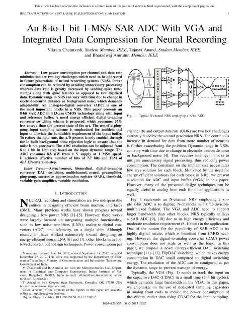
This article has been accepted for inclusion in a future issue of this journal. Content is final as presented, with the exception of pagination.IEEE TRANSACTIONS ON VERY LARGE SCALE INTEGRATION (VLSI) SYSTE<strong>MS</strong> 1<strong>An</strong> 8-<strong>to</strong>-1 <strong>bit</strong> 1-<strong>MS</strong>/s <strong>SAR</strong> <strong>ADC</strong> <strong>With</strong> <strong>VGA</strong> <strong>and</strong><strong>Integrated</strong> <strong>Data</strong> Compression for Neural RecordingVikram Chaturvedi, Student Member, IEEE, Tejasvi <strong>An</strong><strong>and</strong>, Student Member, IEEE,<strong>and</strong> Bharadwaj Amrutur, Member, IEEEAbstract— Low power consumption per channel <strong>and</strong> data rateminimization are two key challenges which need <strong>to</strong> be addressedin future generations of neural recording systems (NRS). Powerconsumption can be reduced by avoiding unnecessary processingwhereas data rate is greatly decreased by sending spike timestampsalong with spike features as opposed <strong>to</strong> raw digitizeddata. Dynamic range in NRS can vary with time due <strong>to</strong> change inelectrode-neuron distance or background noise, which dem<strong>and</strong>sadaptability. <strong>An</strong> analog-<strong>to</strong>-digital converter (<strong>ADC</strong>) is one ofthe most important blocks in a NRS. This paper presents an8-<strong>bit</strong> <strong>SAR</strong> <strong>ADC</strong> in 0.13-µm CMOS technology along with input<strong>and</strong> reference buffer. A novel energy efficient digital-<strong>to</strong>-analogconverter switching scheme is proposed, which consumes 37%less energy than the present state-of-the-art. The use of a pingponginput sampling scheme is emphasized for multichannelinput <strong>to</strong> alleviate the b<strong>and</strong>width requirement of the input buffer.To reduce the data rate, the A/D process is only enabled throughthe in-built background noise rejection logic <strong>to</strong> ensure that thenoise is not processed. The <strong>ADC</strong> resolution can be adjusted from8 <strong>to</strong> 1 <strong>bit</strong> in 1-<strong>bit</strong> step based on the input dynamic range. The<strong>ADC</strong> consumes 8.8 µW from 1 V supply at 1 <strong>MS</strong>/s speed.It achieves effective number of <strong>bit</strong>s of 7.7 <strong>bit</strong>s <strong>and</strong> FoM of42.3 fJ/conversion-step.Index Terms— Asynchronous, biomedical, digital-<strong>to</strong>-analogconverter (DAC) switching, multichannel, neural, preamplifier,ping-pong, successive approximation register (<strong>SAR</strong>), threshold,variable gain amplifier, variable resolution.I. INTRODUCTIONNEURAL recording <strong>and</strong> stimulation are two indispensableentities in designing efficient brain machine interfaces(BMI). Many previous works have shown progress <strong>to</strong>warddesigning a low power NRS [1]–[5]. However, these workswere largely focused on integrating multiple functionality,such as low noise amplifiers (LNA), analog-<strong>to</strong>-digital converters(<strong>ADC</strong>), <strong>and</strong> telemetry, on a single chip. Althoughresearchers have worked extensively <strong>to</strong>ward designing anenergy efficient neural LNA [6] <strong>and</strong> [7], other blocks have followedconventional design techniques. Power consumption perManuscript received June 14, 2012; revised September 14, 2012; acceptedDecember 27, 2012. This work was supported by the Department of InformationTechnology, Ministry of Communication <strong>and</strong> Information Technology,Government of India.V. Chaturvedi <strong>and</strong> B. Amrutur are with the Microelectronics Lab, Departmen<strong>to</strong>f Electrical <strong>and</strong> Computer Engineering, Indian Institute of Science,Bangalore 560012, India (e-mail: vikram@ece.iisc.ernet.in; amrutur@ece.iisc.ernet.in).T. <strong>An</strong><strong>and</strong> is with Oregon State University, Corvallis, OR 97330 USA(e-mail: tejasvian<strong>and</strong>@gmail.com).Color versions of one or more of the figures in this paper are availableonline at http://ieeexplore.ieee.org.Digital Object Identifier 10.1109/TVLSI.2013.2238957Fig. 1.1063–8210/$31.00 © 2013 IEEETypical N-channel NRS employing a K-<strong>bit</strong> <strong>ADC</strong>.channel [8] <strong>and</strong> output data rate (ODR) are two key challengescurrently faced by the second generation NRS. The continuousincrease in dem<strong>and</strong> for data from more number of neuronsis further exacerbating the problem. Dynamic range in NRSscan vary with time due <strong>to</strong> change in electrode-neuron distanceor background noise [4]. This requires intelligent blocks <strong>to</strong>mitigate unnecessary signal processing, thus reducing powerconsumption. The constraint on the implant size necessitateslow area solution for each block. Motivated by the need forenergy efficient solutions for each block in NRS, we presenta solution for <strong>ADC</strong> <strong>and</strong> input buffer (<strong>VGA</strong>) in this paper.However, many of the presented design techniques can beequally useful in analog front-ends for other applications aswell.Fig. 1 represents an N-channel NRS employing a singlek-<strong>bit</strong> <strong>ADC</strong> is <strong>to</strong> digitize N-channels in a time-divisionmultiplexedfashion. The <strong>VGA</strong> <strong>and</strong> <strong>ADC</strong> need <strong>to</strong> supportlarger b<strong>and</strong>width than other blocks. NRS typically utilizesa <strong>SAR</strong> <strong>ADC</strong> [9], [10] due <strong>to</strong> its high energy efficiency <strong>and</strong>moderate resolution requirement (8–10 <strong>bit</strong>s) in the application.One of the reason for the popularity of <strong>SAR</strong> <strong>ADC</strong> is itshighly digital nature, which is benefited from CMOS scaling.However, the digital-<strong>to</strong>-analog converter (DAC) powerconsumption does not scale as well as the logic. In thispaper, we propose a novel energy-efficient DAC switchingtechnique [11]–[13], FlipDAC switching, which makes energyconsumption in DAC small compared <strong>to</strong> digital switchingenergy. The resolution of the <strong>ADC</strong> can be configured as perthe dynamic range <strong>to</strong> prevent wastage of energy.Typically, the <strong>VGA</strong> (Fig. 1) needs <strong>to</strong> track the input onthe capacitive DAC (CDAC) in a small time (2–3 <strong>bit</strong> cycles),which dem<strong>and</strong>s large b<strong>and</strong>width in the <strong>VGA</strong>. In this paper,we emphasize on the use of dedicated sampling capaci<strong>to</strong>rsin analog front ends <strong>to</strong> reduce the power consumption ofthe system, rather than using CDAC for the input sampling.
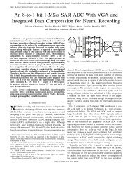
This article has been accepted for inclusion in a future issue of this journal. Content is final as presented, with the exception of pagination.CHATURVEDI et al.: 8-TO-1 BIT 1-<strong>MS</strong>/s <strong>SAR</strong> <strong>ADC</strong> WITH <strong>VGA</strong> AND INTEGRATED DATA COMPRESSION 51) Power Saving in <strong>VGA</strong>: If T vga = α vga · T S , N-<strong>bit</strong> settlingerror is given byV err1 = V ( )ref2 N = V −Tvgaref · exp. (1)R eq · C DACAssuming output resistance R eq = β/I D where β is aconstant dependent on the architecture of the driver <strong>and</strong> I Dis the current consumed in the driverI D,vga,1 = N · ln(2) · β vga · C DAC. (2)α vga · T SNow for ping-pong input sampling α vga = 1InputCDAC−+<strong>SAR</strong><strong>ADC</strong>SpikeSortingDSPFig. 9. <strong>Data</strong>-rate reduction in NRS through the proposed activity-dependentA/D scheme.SthTxI D,vga,2 = N · ln(2) · β vga · C DACT S. (3)The percentage power saving can be calculated asI D,vga,1 − I D,vga,2= (1 − α vga ) · 100%. (4)I D,vga,12) Power Saving in Reference Buffer: If T ref = α ref · T S ,N-<strong>bit</strong> settling error due <strong>to</strong> the reference buffer is given byV err2 = V ( )ref2 N = V −(Tref )/2Nref · exp(5)R eq · C eqwhere C eq is the equivalent capacitance seen by the referencebuffer <strong>and</strong> 50 % of each <strong>bit</strong> cycle (T ref /N) is given for CDACsettlingI D,ref,1 = N · ln(2) · β ref · C eq· 2N. (6)α ref .T SFor ping-pong input sampling α ref = 1I D,ref,2 = N · ln(2) · β ref · C eq· 2N. (7)T SThe percentage power saving can be calculated asI D,ref,1 − I D,ref,2= (1 − α ref ) · 100%. (8)I D,ref,1Hence, for an 8-<strong>bit</strong> <strong>ADC</strong>, with 2 cycles given for samplingin the conventional approach, α vga = 0.2 <strong>and</strong>α ref = 0.8.Hence, 80% power can be saved in the <strong>VGA</strong> <strong>and</strong> 20% powercan be saved in the reference buffer by using ping-pongsampling scheme. Actually the power saving in the <strong>VGA</strong> islarger as the sampling capaci<strong>to</strong>rs (C in0 <strong>and</strong> C in1 in Fig. 8)are much smaller than C DAC (which is used as the samplingcapaci<strong>to</strong>r in the conventional sampling approach).The drawback of this architecture is the need for extrasampling capaci<strong>to</strong>rs. But as their sizes are determined bythermal noise <strong>and</strong> leakage at the <strong>to</strong>p plate switch but notmatching, the area penalty is not significant for moderate resolution(8–10 b) <strong>ADC</strong>s. The leakage from sampling capaci<strong>to</strong>rsbecomes more important consideration for higher resolution<strong>ADC</strong>s in technologies with larger leakage. This architecturealso requires good matching between two sampling paths fora single channel application <strong>and</strong> may need calibration [19].But no such requirement is imposed for multichannel input,as in NRS, where each channel (even or odd) traverses afixed path every time. It also alleviates the concern of dutycycle dis<strong>to</strong>rtion due <strong>to</strong> the half-rate clocking as even- <strong>and</strong>odd-numbered channels are sampled by two different nonoverlappingclocks.(a)Fig. 10. Effective activity fac<strong>to</strong>r. (a) Spike approximated as a triangularwaveform. (b) Important spike features for spike-sorting [15], [21].C. Activity-Dependent A/DThere is a great need <strong>to</strong> reduce the amount of data <strong>to</strong> betransmitted <strong>to</strong> enable chronic recording from more numberof channels. The information in extracellular action potential(EAP) is essentially encoded in spike time-stamps but theamplitude information in EAPs is also important for spikesorting [3]. Simple thresholding is found <strong>to</strong> be equally effectiveas other complex spike detection algorithms [20]. However,representing a spike as a point event causes loss of informationrequired for spike sorting. <strong>An</strong>other way <strong>to</strong> reduce the ODR isthe transmission of important spike features [1], [3]. Fig. 10(b)shows important spike features, A max (the maximum positivespike amplitude), A min (the minimum negative spike amplitude)<strong>and</strong> T pp (the time between A max <strong>and</strong> A min ), that shouldbe kept intact in the output of the <strong>ADC</strong> in a low ODR NRS[15], [21].In this paper, we propose an activity-dependent A/D conversionscheme <strong>to</strong> obviate the processing of background noisebut preserve important spike features. Figs. 9 <strong>and</strong> 10(a) illustratethe proposed scheme. In this, the digitization processis enabled only when the input is larger than the spikedetection threshold S TH . The spike detection threshold S TH isdecided based on the magnitude of the background noise (σ n ),S TH = μ sig + k.σ n where μ sig is the mean of the input <strong>and</strong>k = 3 − 4 so that the probability of the false detection ofthe noise as a spike is small [22]. Note that this schemeis exclusively for the neural recording application where theinformation is in spike time-stamps.Fig. 10(a) depicts the concept of the activity-dependentA/D. The spike is approximated as a triangular waveform withmaximum amplitude A max <strong>and</strong> spike duration T spike . Referring(b)
This article has been accepted for inclusion in a future issue of this journal. Content is final as presented, with the exception of pagination.6 IEEE TRANSACTIONS ON VERY LARGE SCALE INTEGRATION (VLSI) SYSTE<strong>MS</strong><strong>to</strong> Fig. 10(a), the slope the spike can be calculated asm = dVdt= A maxT spike /2 = S THx . (9)Hencex = S TH.T spike(10)2.A maxwhich is the duration of a spike for which the <strong>ADC</strong> does notdigitize the input [Fig. 10(a)].If the <strong>to</strong>tal number of spikes in time T exp is α = S R · T expwhere S R is the spike rate in spikes/s, the effective time (T eff )for which the N <strong>bit</strong> <strong>ADC</strong> operates is given byT eff = α(T spike − 2.x) + [T exp − α(T spike − 2.x)]. (11)N + 1The first term indicates the time for which the <strong>ADC</strong> behavesas a free running <strong>ADC</strong>. The second term in the above equationindicates that the <strong>ADC</strong> operates only for one cycle for spikedetection <strong>and</strong> is idle for remaining N <strong>bit</strong> cycles if the spike isnot detected. The effective activity fac<strong>to</strong>r (EAF) of an N-<strong>bit</strong><strong>ADC</strong> working on activity-based A/D scheme is given byN ( 1 (N + 1 N +S R · T spike · 1 − S ) ) TH. (12)A maxEAF= T eff=T expEquation (12) represents the effective time for which anactivity-dependent <strong>ADC</strong> will be working when compared <strong>to</strong> afree running <strong>ADC</strong>. It represents the reduction in both powerconsumption in the <strong>ADC</strong> <strong>and</strong> ODR of the system. The typicalvalues of T spike <strong>and</strong> SR are 1 ms <strong>and</strong> 100 spikes/s, respectively.Assuming S TH /A max = 0.2, EAF for an 8-<strong>bit</strong> <strong>ADC</strong> can becalculated from 12 as ∼ 0.18, which saves 82% energy <strong>and</strong>ODR over a free running <strong>ADC</strong>.As shown in Fig. 9, the logic is in-built in the <strong>ADC</strong>. CDACis reused for spike thresholding purpose, which obviates theuse of separate DAC for each channel [2]. Equation (12) tellsthat S TH can be increased <strong>to</strong> reduce EAF <strong>and</strong> <strong>to</strong> provide moreimmunity against the background noise but may cause lossof information by missing a spike. Hence, the value of S THshould be decided based on spike sorter’s requirement [23] inaddition <strong>to</strong> the background noise. The proposed <strong>SAR</strong> <strong>ADC</strong> isdesigned <strong>to</strong> be programmable <strong>to</strong> operate either in this modeor free running mode <strong>to</strong> transmit raw data.III. CIRCUIT BLOCKSA. Compara<strong>to</strong>rUnlike many of the previous publications on <strong>SAR</strong> <strong>ADC</strong>where preamplifier is not used before the clocked latch, theuse of a preamplifier is preferred by us for offset <strong>and</strong> kickbacknoise mitigation. Kickback noise is an important concern inthis architecture due <strong>to</strong> the use of small sampling capaci<strong>to</strong>rsfor reducing power consumption in the <strong>VGA</strong>. The preamplifierin <strong>SAR</strong> <strong>ADC</strong> is subjected <strong>to</strong> step input only <strong>and</strong> needs <strong>to</strong>amplify the error just enough for the detection of the sign bythe clocked latch. It relaxes the settling requirement in thepreamplifier.The schematic diagram of the preamplifier is shown inFig. 11. A partial positive feedback is employed <strong>to</strong> reducethe effective output conductance. The load transis<strong>to</strong>rs areVomW1 W2 W2 W1VopVinp Adacp AdacmVinmI0Fig. 11. Schematic diagram of the four-input preamplifier. The preamplifieris employed <strong>to</strong> mitigate the effect of kickback noise on small samplingcapaci<strong>to</strong>rs.sized (W 2 < W 1 ) <strong>to</strong> prevent the effective output conductancefrom becoming negative, even in presence of mismatch. IfW 2 = η · W 1 , the dc voltage gain A v0 <strong>and</strong> the b<strong>and</strong>width ω p ,for a load capacitance C L , can be calculated asA v0 = g m,ing m,w111 − ηI0ω p = g m,w1 · (1 − η)C L.By increasing η <strong>to</strong>ward unity, more voltage gain can beachieved but this makes the preamplifier more sluggish. Wehave chosen η = 0.8 as a tradeoff between voltage gain, speed,<strong>and</strong> stability. The simulated values are A v0 = 14 V/V <strong>and</strong>ω P = 8 MHz. The inputs A dacp <strong>and</strong> A dacm are interchangeable<strong>to</strong> correct the error in the sign of DAC voltage caused duringthe flip step <strong>and</strong> is explained in Section III-B. Individual inputreferredoffsets of two differential pairs in the preamplifier varywith the dynamic operating point of each input pair [24], [25].This variation is desensitized by the current source I 0 [18],especially when effective input <strong>to</strong> the preamplifier is close <strong>to</strong>1 LSB. The latch employed in the compara<strong>to</strong>r is a conventionalsense amplifier-based latch as in [16].B. CDAC Manipulation <strong>and</strong> Sign CorrectionThe FlipDAC switching scheme is explained inSection II-A. During the first DOWN transition, flipping ofthe CDAC is found <strong>to</strong> reduce energy consumption in it. Theflip step comprises of two parts: switching of (<strong>MS</strong>B − 1)thcapaci<strong>to</strong>r <strong>and</strong> manipulating DAC reference rails. This keepsthe DAC capacitance switched in each <strong>bit</strong> cycle same asin [11]. During the flip step, voltage reference rails in CDACare manipulated <strong>to</strong> achieve the desired magnitude of the DACvoltage <strong>and</strong> the logic for this is shown in Fig. 12. WhenFlip signal (Fig. 4) goes HIGH, rails V <strong>and</strong> G are shorted<strong>to</strong>gether <strong>to</strong> V cm input. Based on the sign of the input, V cm1<strong>and</strong> V cm2 rail is shorted <strong>to</strong> either REFP or REFM, whichare outputs of the reference buffer. The proposed <strong>ADC</strong> onlyhas an overhead in digital switching energy over [11] due<strong>to</strong> the manipulation of DAC reference rails otherwise equalcapacitances are switched in every <strong>bit</strong>-cycle. However, as thismanipulation requires a single driver (FLIP), which switchesonly once in a sample period when 1 st <strong>MS</strong>B is logic LOW,the overhead is small.
This article has been accepted for inclusion in a future issue of this journal. Content is final as presented, with the exception of pagination.10 IEEE TRANSACTIONS ON VERY LARGE SCALE INTEGRATION (VLSI) SYSTE<strong>MS</strong>250250200150STH = disabledEAF = 1200150STH = "S0001000"EAF = 0.86100100501 1.1 1.2 1.3 1.4 1.5 1.6x 10 4250501 1.1 1.2 1.3 1.4 1.5 1.6x 10 4250200150100STH = "S0010000"EAF = 0.76200150100STH = "S0100000"EAF = 0.03501 1.1 1.2 1.3 1.4 1.5 1.6x 10 4501 1.1 1.2 1.3 1.4 1.5 1.6x 10 4Fig. 21. Measured digital output of the activity-dependent <strong>ADC</strong>. The x-axis <strong>and</strong> y-axis represent the time in μs <strong>and</strong> the output code, respectively. Theasymmetric rejection of the background noise is due <strong>to</strong> the fact that only five <strong>bit</strong>s were used <strong>to</strong> encode S TH .Relative <strong>ADC</strong> Power ConsumptionRelative Output <strong>Data</strong> Rate10.90.80.70.60.50.40.3σ n=100 mVrmsσ n=33.3 mVrmsσ n=133.3 mVrms0.20 50 100 150 200 25010080604020σ n=100 mV rmsσ n=33.3 mV rmsThreshold S TH(in codes)(a)σ n=133.3 mV rms00 50 100 150 200 250Threshold, S TH(in codes)Fig. 22. Relative reduction in power consumption (P max = 10.7 μW) <strong>and</strong>ODR with different σ n <strong>and</strong> S TH .Higher is the K eff,vga , more power efficient is the <strong>VGA</strong>.Table II presents the comparison of the <strong>VGA</strong> with that inthree state-of-the-art NRSs.(b)V. CONCLUSIONWe presented an 8-<strong>to</strong>-1 <strong>bit</strong>, 1 <strong>MS</strong>/s <strong>SAR</strong> <strong>ADC</strong> in UMC0.13-μm CMOS technology. <strong>An</strong> energy efficient DAC switchingscheme was proposed, which consumes the lowest power<strong>to</strong> date without using extra capaci<strong>to</strong>rs or clock cycles. TheDAC switching scheme consumes 37% less energy than thepresent state-of-the-art. For multichannel input, use of pingponginput sampling was emphasized <strong>to</strong> save power in <strong>VGA</strong><strong>and</strong> reference buffer. The proposed <strong>ADC</strong> also consumes lowerpower in clock buffers as we employ clock of half of thesampling speed. Also the resolution of the <strong>ADC</strong> can be variedbased on the dynamic range <strong>to</strong> avoid unnecessary processing<strong>and</strong> save power.For neural recording application, the ODR was reducedusing the proposed activity-dependent A/D scheme, whichkeeps important spike features preserved in the <strong>ADC</strong> output.This scheme saves both power <strong>and</strong> area when compared <strong>to</strong>spike feature extraction schemes, which employ complicatedon-chip DSP. The savings in power consumption of the <strong>ADC</strong><strong>and</strong> ODR due <strong>to</strong> the scheme are calculated <strong>and</strong> expressedin term of EAF. <strong>An</strong> experiment with the real neural datawas carried out <strong>to</strong> show the usefulness of the scheme forthe application. <strong>An</strong> emphasis was put on the requirement oflarge programmable voltage gain in the <strong>VGA</strong> for NRS. Thepresented <strong>VGA</strong> provides a voltage gain of 8 dB-35 dB ineight steps.The presented <strong>SAR</strong> <strong>ADC</strong> consumes 8.8 μW from 1 Vsupply <strong>and</strong> achieves ENOB of 7.7 <strong>bit</strong> for a near Nyquistinput at 1 <strong>MS</strong>/s speed. FlipDAC switching technique makesenergy consumption in the DAC small compared <strong>to</strong> digitalswitching energy. The DAC switching scheme will prove <strong>to</strong>be more beneficial in higher resolution <strong>and</strong> higher speed <strong>SAR</strong><strong>ADC</strong>s where the DAC switching energy is more comparable<strong>to</strong> the digital switching energy. The <strong>ADC</strong> achieves a FoM of42.3 fJ/conversion. The power consumption in the <strong>ADC</strong> is
This article has been accepted for inclusion in a future issue of this journal. Content is final as presented, with the exception of pagination.CHATURVEDI et al.: 8-TO-1 BIT 1-<strong>MS</strong>/s <strong>SAR</strong> <strong>ADC</strong> WITH <strong>VGA</strong> AND INTEGRATED DATA COMPRESSION 11dominated by digital switching, which will only improve withvoltage <strong>and</strong> technology scaling.REFERENCES[1] M. S. Chae, Z. Yang, M. Yuce, L. Hoang, <strong>and</strong> W. Liu, “A 128-channel6 mW wireless neural recording IC with spike feature extraction <strong>and</strong>UWB transmitter,” IEEE Trans. Neural Syst. Rehabil. Eng., vol. 17,no. 4, pp. 312–321, Aug. 2009.[2] R. Harrison, R. J. Kier, C. A. Chestek, V. Gilja, P. Nuyujukian, S. Ryu,B. Greger, F. Solzbacher, <strong>and</strong> K. V. Shenoy, “Wireless neural recordingwith single low-power integrated circuit,” IEEE Trans. Neural Syst.Rehabil. Eng., vol. 17, no. 4, pp. 322–329, Aug. 2009.[3] A. Sodagar, G. Perlin, Y. Yao, K. Najafi, <strong>and</strong> K. Wise, “<strong>An</strong> implantable64-channel wireless microsystem for single-unit neural recording,” IEEEJ. Solid-State Circuits, vol. 44, no. 9, pp. 2591–2604, Sep. 2009.[4] M. Yin <strong>and</strong> M. Ghovanloo, “A flexible clockless 32-ch simultaneouswireless neural recording system with adjustable resolution,” in Proc.IEEE Int. Solid-State Circuits Conf., Dig. Tech. Papers, Feb. 2009,pp. 432–433.[5] M. Azin, D. Guggenmos, S. Barbay, R. Nudo, <strong>and</strong> P. Mohseni, “Abattery-powered activity-dependent intracortical microstimulation IC forbrain-machine-brain interface,” IEEE J. Solid-State Circuits, vol. 46,no. 4, pp. 731–745, Apr. 2011.[6] R. Harrison <strong>and</strong> C. Charles, “A low-power low-noise CMOS amplifierfor neural recording applications,” IEEE J. Solid-State Circuits, vol. 38,no. 6, pp. 958–965, Jun. 2003.[7] V. Chaturvedi <strong>and</strong> B. Amrutur, “<strong>An</strong> area-efficient noise-adaptive neuralamplifier in 130 nm CMOS technology,” IEEE J. Emerg. Sel. TopicsCircuits Syst., vol. 1, no. 4, pp. 536–545, Dec. 2011.[8] W.-S. Liew, X. Zou, L. Yao, <strong>and</strong> Y. Lian, “A 1-V 60-μW 16-channelinterface chip for implantable neural recording,” in Proc. IEEE Cus<strong>to</strong>mIntegr. Circuits Conf., Sep. 2009, pp. 507–510.[9] J. McCreary <strong>and</strong> P. Gray, “All-MOS charge redistribution analog-<strong>to</strong>digitalconversion techniques. I,” IEEE J. Solid-State Circuits, vol. 10,no. 6, pp. 371–379, Dec. 1975.[10] G. Promitzer, “12-<strong>bit</strong> low-power fully differential switched capaci<strong>to</strong>rnoncalibrating successive approximation <strong>ADC</strong> with 1<strong>MS</strong>/s,” IEEE J.Solid-State Circuits, vol. 36, no. 7, pp. 1138–1143, Jul. 2001.[11] Y. Zhu. C.-H. Chan, U.-F. Chio, S.-W. Sin, U. Seng-Pan, R. P. Martins,<strong>and</strong> F. Maloberti, “A 10-<strong>bit</strong> 100-<strong>MS</strong>/s reference-free <strong>SAR</strong> <strong>ADC</strong> in 90 nmCMOS,” IEEE J. Solid-State Circuits, vol. 45, no. 6, pp. 1111–1121, Jun.2010.[12] M. van Elzakker, E. van Tuijl, P. Geraedts, D. Schinkel, E. Klumperink,<strong>and</strong> B. Nauta, “A 1.9 μW 4.4 fJ/conversion-step 10 b 1 <strong>MS</strong>/s chargeredistribution<strong>ADC</strong>,” in Proc. IEEE Int. Solid-State Circuits Conf., Dig.Tec. Papers, Feb. 2008, pp. 244–610.[13] Y.-K. Chang, C.-S. Wang, <strong>and</strong> C.-K. Wang, “A 8-<strong>bit</strong> 500-KS/s low power<strong>SAR</strong> <strong>ADC</strong> for bio-medical applications,” in Proc. IEEE Asian Solid-State Circuits Conf., Nov. 2007, pp. 228–231.[14] B. Malki, T. Yamamo<strong>to</strong>, B. Verbruggen, P. Wambacq, <strong>and</strong> J. Craninckx,“A 70 dB DR 10b 0-<strong>to</strong>-80<strong>MS</strong>/s current-integrating <strong>SAR</strong> <strong>ADC</strong> withadaptive dynamic range,” in Proc. IEEE Int. Solid-State Circuits Conf.Dig. Tech. Papers, Feb. 2012, pp. 470–472.[15] R. H. Olsson <strong>and</strong> K. Wise, “A three-dimensional neural recordingmicrosystem with implantable data compression circuitry,” IEEE J.Solid-State Circuits, vol. 40, no. 12, pp. 2796–2804, Dec. 2005.[16] B. Ginsburg <strong>and</strong> A. Ch<strong>and</strong>rakasan, “500-<strong>MS</strong>/s 5-<strong>bit</strong> <strong>ADC</strong> in 65-nmCMOS with split capaci<strong>to</strong>r array DAC,” IEEE J. Solid-State Circuits,vol. 42, no. 4, pp. 739–747, Apr. 2007.[17] T. <strong>An</strong><strong>and</strong>, V. Chaturvedi, <strong>and</strong> B. Amrutur, “Energy efficient asymmetricbinary search switching technique for <strong>SAR</strong> <strong>ADC</strong>,” Electron. Lett.,vol. 46, no. 22, pp. 1487–1488, Oct. 2010.[18] C.-C. Liu, S.-J. Chang, G.-Y. Huang, <strong>and</strong> Y.-Z. Lin, “A 10-<strong>bit</strong> 50-<strong>MS</strong>/s<strong>SAR</strong> <strong>ADC</strong> with a mono<strong>to</strong>nic capaci<strong>to</strong>r switching procedure,” IEEE J.Solid-State Circuits, vol. 45, no. 4, pp. 731–740, Apr. 2010.[19] A. Petraglia <strong>and</strong> S. Mitra, “<strong>An</strong>alysis of mismatch effects amongA/D converters in a time-interleaved waveform digitizer,” IEEE Trans.Instrum. Meas., vol. 40, no. 5, pp. 831–835, Oct. 1991.[20] I. Obeid <strong>and</strong> P. D. Wolf, “Evaluation of spike-detection algorithms for abrain-machine interface application,” IEEE Trans. Biomed. Eng., vol. 51,no. 6, pp. 905–911, Jun. 2004.[21] J. Vibert <strong>and</strong> J. Costa, “Spike separation in multiunit records: Amultivariate analysis of spike descriptive parameters,” Electroencephalograph.Clinical Neurophysiol., vol. 47, no. 2, pp. 172–182, 1979.[22] H. Semmaoui, J. Drolet, A. Lakhssassi, <strong>and</strong> M. Sawan, “Setting adaptivespike detection threshold for smoothed-teo based on robust statisticstheory,” IEEE Trans. Biomed. Eng., vol. 59, no. 2, pp. 474–482,Feb. 2012.[23] S. O’Driscoll, K. Shenoy, <strong>and</strong> T. Meng, “Adaptive resolution <strong>ADC</strong> arrayfor an implantable neural sensor,” IEEE Trans. Biomed. Circuits Syst.,vol. 5, no. 2, pp. 120–130, Apr. 2011.[24] L. Sumanen, M. Waltari, <strong>and</strong> K. Halonen, “A mismatch insensitiveCMOS dynamic compara<strong>to</strong>r for pipeline A/D converters,” in Proc. 7thIEEE Int. Conf. Electron., Circuits Syst., vol. 1. Dec. 2000, pp. 32–35.[25] V. Katyal, R. L. Geiger, <strong>and</strong> D. J. Chen, “A new high precision lowoffset dynamic compara<strong>to</strong>r for high resolution high speed <strong>ADC</strong>s,” inProc. IEEE Asia Pacific Conf. Circuits Syst., Dec. 2006, pp. 5–8.[26] W. Wattanapanitch <strong>and</strong> R. Sarpeshkar, “A low-power 32-channel digitallyprogrammable neural recording integrated circuit,” IEEE Trans.Biomed. Circuits Syst., vol. 5, no. 6, pp. 592–602, Dec. 2011.[27] M. Scott, B. Boser, <strong>and</strong> K. Pister, “<strong>An</strong> ultralow-energy adc for smartdust,” IEEE J. Solid-State Circuits, vol. 38, no. 7, pp. 1123–1129,Jul. 2003.[28] N. Verma <strong>and</strong> A. Ch<strong>and</strong>rakasan, “<strong>An</strong> ultra low energy 12-<strong>bit</strong> rateresolutionscalable <strong>SAR</strong> <strong>ADC</strong> for wireless sensor nodes,” IEEE J. Solid-State Circuits, vol. 42, no. 6, pp. 1196–1205, Jun. 2007.[29] M. Yip <strong>and</strong> A. Ch<strong>and</strong>rakasan, “A resolution-reconfigurable 5-<strong>to</strong>-10b 0.4-<strong>to</strong>-V power scalable <strong>SAR</strong> <strong>ADC</strong>,” in Proc. IEEE Int. Solid-State CircuitsConf. Dig. Tech. Papers, Feb. 2011, pp. 190–192.Vikram Chaturvedi (S’10) received the B.E. degreein electronics <strong>and</strong> telecommunication from the ShriGovindram Seksaria Institute of Technology <strong>and</strong> Science,Indore, India, in 2006. He is currently pursuingthe Ph.D. degree with the Electrical CommunicationEngineering Department, Indian Institute of Science,Bangalore, India.He was with ERC, Tata Mo<strong>to</strong>rs Ltd., where hewas involved in research on remote keyless entrysystem from 2006 <strong>to</strong> 2007. He presented a paper atthe SRP session of ISSCC 2010. His current researchinterests include adaptive biomedical systems, energy-efficient data converters,<strong>and</strong> high-speed serial interfaces.Mr. Chaturvedi was a recipient of the first Student Travel Grants byIEEE Solid-State Circuit Society (SSCS) as a recognition of early careeraccomplishments on solid-state circuits. He is a member of the SSCS <strong>and</strong>the IEEE Circuits <strong>and</strong> Systems Society.Tejasvi <strong>An</strong><strong>and</strong> (S’12) received the B.Tech. degreein electronics <strong>and</strong> communication from Guru GobindSingh Indraprastha University, New Delhi, India,<strong>and</strong> the M.Tech. degree in electronics design <strong>and</strong>technology from the Indian Institute of Science,Bangalore, India, in 2006 <strong>and</strong> 2008, respectively. Heis currently pursuing the Ph.D. degree with OregonState University, Corvallis.He was with the Cosmic Circuits <strong>and</strong> MicroelectronicsLabora<strong>to</strong>ry, Indian Institute of Science. Hiscurrent research interests include high-speed serialinterfaces, frequency synthesizers, <strong>and</strong> data converters.Bharadwaj Amrutur (M’08) received the B.Tech.degree in computer science <strong>and</strong> engineering fromthe Indian Institute of Technology Bombay, Mumbai,India, in 1990, <strong>and</strong> the M.S. <strong>and</strong> Ph.D. degrees inelectrical engineering from Stanford University, PaloAl<strong>to</strong>, CA, in 1994 <strong>and</strong> 1999, respectively.He was with Bell Labs, Agilent Labs, <strong>and</strong> GreenfieldNetworks. He is currently an Associate Professorwith the Department of Electrical CommunicationEngineering, Indian Institute of Science,Bangalore, India, where he is involved in researchon VLSI circuits <strong>and</strong> systems.