An 8-to-1 bit 1-MS/s SAR ADC With VGA and Integrated Data ...
An 8-to-1 bit 1-MS/s SAR ADC With VGA and Integrated Data ...
An 8-to-1 bit 1-MS/s SAR ADC With VGA and Integrated Data ...

Create successful ePaper yourself
Turn your PDF publications into a flip-book with our unique Google optimized e-Paper software.
This article has been accepted for inclusion in a future issue of this journal. Content is final as presented, with the exception of pagination.<br />
IEEE TRANSACTIONS ON VERY LARGE SCALE INTEGRATION (VLSI) SYSTE<strong>MS</strong> 1<br />
<strong>An</strong> 8-<strong>to</strong>-1 <strong>bit</strong> 1-<strong>MS</strong>/s <strong>SAR</strong> <strong>ADC</strong> <strong>With</strong> <strong>VGA</strong> <strong>and</strong><br />
<strong>Integrated</strong> <strong>Data</strong> Compression for Neural Recording<br />
Vikram Chaturvedi, Student Member, IEEE, Tejasvi <strong>An</strong><strong>and</strong>, Student Member, IEEE,<br />
<strong>and</strong> Bharadwaj Amrutur, Member, IEEE<br />
Abstract— Low power consumption per channel <strong>and</strong> data rate<br />
minimization are two key challenges which need <strong>to</strong> be addressed<br />
in future generations of neural recording systems (NRS). Power<br />
consumption can be reduced by avoiding unnecessary processing<br />
whereas data rate is greatly decreased by sending spike timestamps<br />
along with spike features as opposed <strong>to</strong> raw digitized<br />
data. Dynamic range in NRS can vary with time due <strong>to</strong> change in<br />
electrode-neuron distance or background noise, which dem<strong>and</strong>s<br />
adaptability. <strong>An</strong> analog-<strong>to</strong>-digital converter (<strong>ADC</strong>) is one of<br />
the most important blocks in a NRS. This paper presents an<br />
8-<strong>bit</strong> <strong>SAR</strong> <strong>ADC</strong> in 0.13-µm CMOS technology along with input<br />
<strong>and</strong> reference buffer. A novel energy efficient digital-<strong>to</strong>-analog<br />
converter switching scheme is proposed, which consumes 37%<br />
less energy than the present state-of-the-art. The use of a pingpong<br />
input sampling scheme is emphasized for multichannel<br />
input <strong>to</strong> alleviate the b<strong>and</strong>width requirement of the input buffer.<br />
To reduce the data rate, the A/D process is only enabled through<br />
the in-built background noise rejection logic <strong>to</strong> ensure that the<br />
noise is not processed. The <strong>ADC</strong> resolution can be adjusted from<br />
8 <strong>to</strong> 1 <strong>bit</strong> in 1-<strong>bit</strong> step based on the input dynamic range. The<br />
<strong>ADC</strong> consumes 8.8 µW from 1 V supply at 1 <strong>MS</strong>/s speed.<br />
It achieves effective number of <strong>bit</strong>s of 7.7 <strong>bit</strong>s <strong>and</strong> FoM of<br />
42.3 fJ/conversion-step.<br />
Index Terms— Asynchronous, biomedical, digital-<strong>to</strong>-analog<br />
converter (DAC) switching, multichannel, neural, preamplifier,<br />
ping-pong, successive approximation register (<strong>SAR</strong>), threshold,<br />
variable gain amplifier, variable resolution.<br />
I. INTRODUCTION<br />
NEURAL recording <strong>and</strong> stimulation are two indispensable<br />
entities in designing efficient brain machine interfaces<br />
(BMI). Many previous works have shown progress <strong>to</strong>ward<br />
designing a low power NRS [1]–[5]. However, these works<br />
were largely focused on integrating multiple functionality,<br />
such as low noise amplifiers (LNA), analog-<strong>to</strong>-digital converters<br />
(<strong>ADC</strong>), <strong>and</strong> telemetry, on a single chip. Although<br />
researchers have worked extensively <strong>to</strong>ward designing an<br />
energy efficient neural LNA [6] <strong>and</strong> [7], other blocks have followed<br />
conventional design techniques. Power consumption per<br />
Manuscript received June 14, 2012; revised September 14, 2012; accepted<br />
December 27, 2012. This work was supported by the Department of Information<br />
Technology, Ministry of Communication <strong>and</strong> Information Technology,<br />
Government of India.<br />
V. Chaturvedi <strong>and</strong> B. Amrutur are with the Microelectronics Lab, Department<br />
of Electrical <strong>and</strong> Computer Engineering, Indian Institute of Science,<br />
Bangalore 560012, India (e-mail: vikram@ece.iisc.ernet.in; amrutur@ece.iisc.ernet.in).<br />
T. <strong>An</strong><strong>and</strong> is with Oregon State University, Corvallis, OR 97330 USA<br />
(e-mail: tejasvian<strong>and</strong>@gmail.com).<br />
Color versions of one or more of the figures in this paper are available<br />
online at http://ieeexplore.ieee.org.<br />
Digital Object Identifier 10.1109/TVLSI.2013.2238957<br />
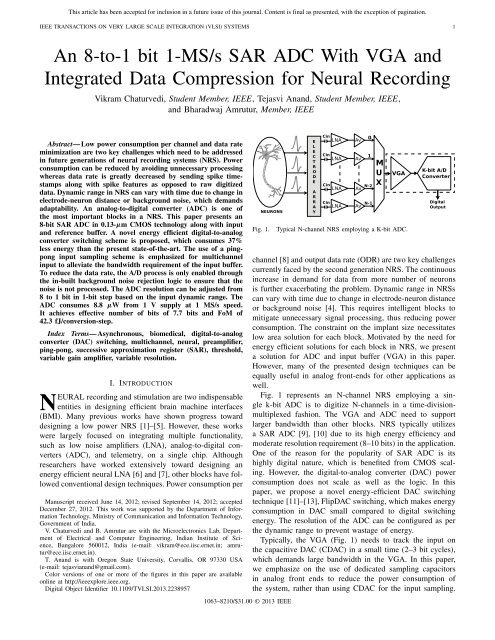
Fig. 1.<br />
1063–8210/$31.00 © 2013 IEEE<br />
Typical N-channel NRS employing a K-<strong>bit</strong> <strong>ADC</strong>.<br />
channel [8] <strong>and</strong> output data rate (ODR) are two key challenges<br />
currently faced by the second generation NRS. The continuous<br />
increase in dem<strong>and</strong> for data from more number of neurons<br />
is further exacerbating the problem. Dynamic range in NRSs<br />
can vary with time due <strong>to</strong> change in electrode-neuron distance<br />
or background noise [4]. This requires intelligent blocks <strong>to</strong><br />
mitigate unnecessary signal processing, thus reducing power<br />
consumption. The constraint on the implant size necessitates<br />
low area solution for each block. Motivated by the need for<br />
energy efficient solutions for each block in NRS, we present<br />
a solution for <strong>ADC</strong> <strong>and</strong> input buffer (<strong>VGA</strong>) in this paper.<br />
However, many of the presented design techniques can be<br />
equally useful in analog front-ends for other applications as<br />
well.<br />
Fig. 1 represents an N-channel NRS employing a single<br />
k-<strong>bit</strong> <strong>ADC</strong> is <strong>to</strong> digitize N-channels in a time-divisionmultiplexed<br />
fashion. The <strong>VGA</strong> <strong>and</strong> <strong>ADC</strong> need <strong>to</strong> support<br />
larger b<strong>and</strong>width than other blocks. NRS typically utilizes<br />
a <strong>SAR</strong> <strong>ADC</strong> [9], [10] due <strong>to</strong> its high energy efficiency <strong>and</strong><br />
moderate resolution requirement (8–10 <strong>bit</strong>s) in the application.<br />
One of the reason for the popularity of <strong>SAR</strong> <strong>ADC</strong> is its<br />
highly digital nature, which is benefited from CMOS scaling.<br />
However, the digital-<strong>to</strong>-analog converter (DAC) power<br />
consumption does not scale as well as the logic. In this<br />
paper, we propose a novel energy-efficient DAC switching<br />
technique [11]–[13], FlipDAC switching, which makes energy<br />
consumption in DAC small compared <strong>to</strong> digital switching<br />
energy. The resolution of the <strong>ADC</strong> can be configured as per<br />
the dynamic range <strong>to</strong> prevent wastage of energy.<br />
Typically, the <strong>VGA</strong> (Fig. 1) needs <strong>to</strong> track the input on<br />
the capacitive DAC (CDAC) in a small time (2–3 <strong>bit</strong> cycles),<br />
which dem<strong>and</strong>s large b<strong>and</strong>width in the <strong>VGA</strong>. In this paper,<br />
we emphasize on the use of dedicated sampling capaci<strong>to</strong>rs<br />
in analog front ends <strong>to</strong> reduce the power consumption of<br />
the system, rather than using CDAC for the input sampling.
This article has been accepted for inclusion in a future issue of this journal. Content is final as presented, with the exception of pagination.<br />
2 IEEE TRANSACTIONS ON VERY LARGE SCALE INTEGRATION (VLSI) SYSTE<strong>MS</strong><br />
<strong>VGA</strong> REFBFR<br />
REFP<br />
Vcm<br />
REFM<br />
Vip0<br />
Vim0<br />
Vip1<br />
Vim1<br />
CDAC<br />
Vinp<br />
Vdacp<br />
Vdacm<br />
Vinm<br />
+<br />
-<br />
+ Av<br />
-<br />
compara<strong>to</strong>r<br />
Vop<br />
Flip<br />
Vip<br />
Vim<br />
clk=Fs/2<br />
Switch Control<br />
Pingpong<br />
Sampling<br />
Sth<br />
Threshold<br />
N[2:0]<br />
<strong>and</strong> Noise noise<br />
Sth<br />
Estimation<br />
Cin0<br />
Cin1<br />
DR<br />
Vom<br />
LATCH<br />
outp<br />
outm<br />
<strong>Data</strong> Register<br />
STB<br />
clk<br />
Asynchronous<br />
<strong>SAR</strong> Logic<br />
Digital Output<br />
Fig. 2. Block diagram of the proposed <strong>SAR</strong> <strong>ADC</strong> with an on-chip voltage<br />
reference buffer (REFBFR).<br />
We also recommend employing a ping-pong input sampling<br />
architecture [14] <strong>to</strong> alleviate the b<strong>and</strong>width requirement of the<br />
<strong>VGA</strong>. It is explained in more detail in Section II-B. The amplitude<br />
of the maximum detectable signal varies with neuronelectrode<br />
distance <strong>and</strong> probe impedance, which is frequency<br />
dependent. A fixed gain in NRS will either under-utilize the<br />
<strong>ADC</strong> dynamic range or causes clipping of the peaks. Hence,<br />
we emphasize a large programmable range in voltage gain of<br />
the <strong>VGA</strong>. The designed <strong>VGA</strong> has voltage gain programmable<br />
from 8 <strong>to</strong> 35 dB in eight steps.<br />
NRS generate tremendous amount of data due <strong>to</strong> chronic<br />
recording from a large number of neurons [3]. The transmission<br />
of this large amount of data through a wireless link<br />
poses serious threat <strong>to</strong> the scalability <strong>and</strong> power efficiency<br />
of BMI. Spike feature extraction [1] <strong>and</strong> simple thresholding<br />
[2] are two popular ways through which researchers have<br />
tried <strong>to</strong> reduce output data rate. However, the former needs<br />
extra hardware <strong>and</strong> power whereas the latter can cause loss<br />
of information for spike sorting. The present low ODR NRSs<br />
typically need an extra spike detection block, e.g., one DAC<br />
per channel [2], which consumes large area. In this paper,<br />
we merge spike detection logic in<strong>to</strong> the <strong>ADC</strong>, reusing the<br />
CDAC in it. This scheme not only mitigates the processing of<br />
the background noise <strong>to</strong> reduce the ODR but also preserves<br />
important spike features, which are required for the spike<br />
sorting [15]. It also helps in reducing power consumption <strong>and</strong><br />
area of NRS.<br />
This paper is organized as follows. Section II presents the<br />
architecture of the <strong>ADC</strong>, ping-pong input sampling scheme <strong>to</strong><br />
relax <strong>VGA</strong> specification <strong>and</strong> activity-dependent A/D scheme<br />
<strong>to</strong> reduce ODR. Section II also explains the energy efficient<br />
DAC switching technique, FlipDAC. Section III discusses the<br />
circuit implementation of various blocks. Section IV presents<br />
the measured results from a chip fabricated in UMC 0.13-μm<br />
CMOS technology. Section V concludes this paper.<br />
II. <strong>ADC</strong> ARCHITECTURE<br />
The block diagram of the proposed <strong>SAR</strong> <strong>ADC</strong> is shown in<br />
Fig. 2. Fully differential input <strong>and</strong> reference voltages are used.<br />
The reference DAC <strong>and</strong> sampling capaci<strong>to</strong>rs are segregated<br />
<strong>to</strong> gain advantages explained in Section II-B. A four-input<br />
preamplifier is used in the compara<strong>to</strong>r <strong>to</strong> mitigate the effect of<br />
kickback noise on sampling capaci<strong>to</strong>rs (C in0,1 ). A master clock<br />
NEXT<br />
Vcm<br />
2C C C<br />
Vcm<br />
2C C C<br />
Vcm<br />
E=0<br />
+<br />
−<br />
Vdac=0<br />
2C<br />
Vcm<br />
2C<br />
V<br />
Vcm+V/4<br />
C C<br />
+<br />
C C<br />
Vcm-V/4<br />
E=0.5<br />
(a)<br />
−<br />
Vdac=V/2<br />
V<br />
2C<br />
Vcm<br />
Vcm+V/4<br />
2C C C<br />
C C<br />
+<br />
+<br />
Vcm<br />
Vcm<br />
−<br />
−<br />
2C C C Vdac=0<br />
C C Vdac=V/2<br />
Vcm<br />
Vcm-V/4<br />
2C<br />
E=0 E=0.5<br />
(b)<br />
UP<br />
DOWN<br />
UP<br />
DOWN<br />
2C C Vdac=3V/4<br />
Vcm+3V/8 C<br />
+<br />
Vcm<br />
−<br />
Vcm-3V/8 C<br />
2C C<br />
E=1/8<br />
2C C Vdac=V/4<br />
Vcm+V/8 C<br />
+<br />
Vcm<br />
−<br />
Vcm-V/8 C<br />
2C C<br />
2C C<br />
Vdac=3V/4<br />
Vcm+3V/8 C<br />
+<br />
Vcm<br />
−<br />
Vcm-3V/8 C<br />
2C C<br />
Vcm<br />
2C<br />
2C<br />
V<br />
V<br />
V<br />
C Vcm-V/8<br />
C<br />
+ -Vdac=V/4<br />
V<br />
C<br />
V<br />
V<br />
V<br />
E=5/8<br />
E=1/8<br />
−<br />
C FlipDac<br />
Vcm+V/8<br />
E=1/8<br />
Fig. 3. (a) DAC switching in a 3-<strong>bit</strong> <strong>SAR</strong> <strong>ADC</strong> [11]. (b) FlipDAC switching.<br />
In the figure, V = 2·V cm = V ref <strong>and</strong> the unit of energy consumption is C.Vref 2 .<br />
Vip-Vin<br />
purge<br />
FlipDac<br />
Vdacp-Vdacm<br />
1 1 1 0 1 0 0 1<br />
Flip<br />
Strobe<br />
Vref-(Vip-Vin)<br />
Vdacm-Vdacp<br />
sign b2 b1 b0 sign b2 b1 b0<br />
Fig. 4. Input digitization through the proposed FlipDAC switching technique.<br />
In the second case, output 1001 is resolved indirectly by tracking 1110 by<br />
V dacp − V dacm .<br />
of only half the sampling speed is used due <strong>to</strong> the ping-pong<br />
input sampling architecture. It reduces the power consumption<br />
in clock buffers by 2× <strong>and</strong> decreases the <strong>to</strong>tal system power<br />
consumption. To reduce output data rate, the detection of the<br />
neural spikes is achieved using spike threshold S TH ,which<br />
is calculated based on the background noise <strong>and</strong> is s<strong>to</strong>red in<br />
registers. This is explained more in Section II-C. The dynamic<br />
range (DR) decides the resolution setting (N) of the <strong>ADC</strong>. <strong>An</strong><br />
on-chip voltage reference buffer is implemented <strong>to</strong> provide<br />
clean <strong>and</strong> stable voltage reference <strong>to</strong> the <strong>ADC</strong>.<br />
A. FlipDAC Switching<br />
Of late, there has been a lot of interest in energy efficient<br />
DAC switching techniques for CDAC [11]–[13]. It has been<br />
shown that the DOWN transitions take more energy than
This article has been accepted for inclusion in a future issue of this journal. Content is final as presented, with the exception of pagination.<br />
CHATURVEDI et al.: 8-TO-1 BIT 1-<strong>MS</strong>/s <strong>SAR</strong> <strong>ADC</strong> WITH <strong>VGA</strong> AND INTEGRATED DATA COMPRESSION 3<br />
Fig. 5.<br />
Proposed FlipDAC switching scheme for a 4-<strong>bit</strong> <strong>SAR</strong> <strong>ADC</strong> <strong>and</strong> energy cost comparison with [11] for each step in the binary search tree.<br />
UP transitions in the digitization process [16]. This is the<br />
reason that the energy consumption for a code near the center<br />
of the <strong>ADC</strong> dynamic range is greater than that of a code<br />
<strong>to</strong>ward extremes. For a 10-<strong>bit</strong> <strong>ADC</strong>, code 511 <strong>and</strong> code 512<br />
require maximum energy, whereas code 0 <strong>and</strong> code 1023 take<br />
minimum energy [11]. The energy drawn from the reference<br />
can be reduced if it is possible <strong>to</strong> resolve an input through<br />
fewer DOWN transitions. Even if the number of DOWN<br />
transitions is not smaller than that of UP transitions, the energy<br />
consumption can be lowered by pushing DOWN transitions<br />
<strong>to</strong>ward LSBs.<br />
Fig. 3(a) shows the switching scheme proposed in [11]<br />
for a 3-<strong>bit</strong> <strong>SAR</strong> <strong>ADC</strong>. The DOWN transition draws 5 times<br />
more energy from the reference compared <strong>to</strong> the UP transition.<br />
Fig. 3(b) presents the proposed switching technique. For the<br />
DOWN transition step, the energy drawn from the reference is<br />
5 times smaller than that in Fig. 3(a). This step is performed<br />
by switching C <strong>and</strong> re-arranging DAC reference rails so as<br />
not <strong>to</strong> degrade digital switching energy <strong>and</strong> is explained in<br />
detail in Section III-B. The proposed scheme is overall 33%<br />
more energy efficient than Fig. 3(a). Note that the DAC<br />
voltage achieved in the DOWN transition is negative of the<br />
desired value (V dac =−V/4). The sign of the DAC voltage<br />
is corrected by either interchanging the two DAC inputs <strong>to</strong><br />
the compara<strong>to</strong>r or by comparing this negative DAC voltage<br />
with the negative of the sampled input voltage. The former<br />
approach is preferred as the latter will flip the offset of the<br />
compara<strong>to</strong>r, which can affect the linearity of the <strong>ADC</strong>.<br />
This reduction in the energy consumption is achieved by<br />
mapping the input voltage <strong>to</strong> a digital code, which is more<br />
energy efficient than the actual code for the input. Fig. 4<br />
explains this for a 4-<strong>bit</strong> <strong>SAR</strong> <strong>ADC</strong>. If b 2 is detected as logic<br />
HIGH, V dacp -V dacm tracks V ip − V in in the conventional way.<br />
However, if b 2 is detected as logic LOW, Flip goes high <strong>and</strong>,<br />
V dacp <strong>and</strong> V dacm interchange their roles. The remaining tracking<br />
of the input V ip −V in is then carried out by V dacm −V dacp .It<br />
is equivalent <strong>to</strong> resolving V ref −(V ip −V in ) by V dacp −V dacm in<br />
remaining <strong>bit</strong> cycles. This maps the input <strong>to</strong> a higher digital<br />
code <strong>and</strong> helps in reducing the number of times CDAC is<br />
discharged, especially during <strong>MS</strong>Bs. As shown in Fig. 4,<br />
output code 1001 is resolved indirectly by tracking code 1110<br />
by the CDAC. This results in fewer discharging steps than the<br />
case when CDAC resolves 1001 directly.<br />
Fig. 5 represents the switching scheme for a 4-<strong>bit</strong> <strong>ADC</strong> for<br />
V ip > V in . Note that 2 nd <strong>MS</strong>B capaci<strong>to</strong>r (2C) is the replica<br />
of remaining two LSB capaci<strong>to</strong>rs. First, DOWN transition<br />
in Fig. 5 again illustrates the concept of FlipDAC switching<br />
technique. The FlipDAC step does not take any extra clock
This article has been accepted for inclusion in a future issue of this journal. Content is final as presented, with the exception of pagination.<br />
4 IEEE TRANSACTIONS ON VERY LARGE SCALE INTEGRATION (VLSI) SYSTE<strong>MS</strong><br />
2<br />
Energy consumed (C.V ) ref<br />
220<br />
200<br />
180<br />
160<br />
140<br />
120<br />
100<br />
[Zhu]<br />
E avg<br />
=142<br />
[This paper]<br />
E avg<br />
=106<br />
E avg<br />
=170<br />
37.5 %<br />
[<strong>An</strong><strong>and</strong>]<br />
[zhu]<br />
This paper<br />
[an<strong>and</strong>]<br />
25.3 %<br />
100 200 300 400 500 600 700 800 900 1000<br />
Output Code (in LSB)<br />
Fig. 6. Comparison of CDAC switching energy with [11] <strong>and</strong> [17] for a<br />
10-<strong>bit</strong> <strong>SAR</strong> <strong>ADC</strong>.<br />
TABLE I<br />
DAC SWITCHING ENERGY COMPARISON FOR A 10-b <strong>SAR</strong> <strong>ADC</strong><br />
Spec. [17] [18] [11] This Scheme<br />
Avg. Energy (C.Vref 2 ) 142 255.5 170 106<br />
Energy Saving 25.3 % 58.6 % 37.5 % –<br />
cycle <strong>and</strong> hence speed is not compromised. The flipping of<br />
the CDAC is done only for the first DOWN transition by<br />
making use of the symmetric structure of the CDAC, for both<br />
UP <strong>and</strong> DOWN transitions, from this node. The splitting of<br />
(<strong>MS</strong>B − 1)th capaci<strong>to</strong>r helps in implementing binary search<br />
algorithm, after flipping, without incurring extra time <strong>and</strong><br />
switching. The energy consumption during various steps for<br />
a 4-<strong>bit</strong> <strong>ADC</strong> is also compared with [11, Fig. 5]. The number<br />
in the circle represents the <strong>to</strong>tal number of unit capaci<strong>to</strong>rs<br />
connected <strong>to</strong> V ref . The relative energy costs are shown on the<br />
arrows.<br />
Fig. 6 depicts the comparison of the energy drawn from<br />
the reference for each code in a 10-<strong>bit</strong> <strong>SAR</strong> <strong>ADC</strong> in [11]<br />
<strong>and</strong> [17], <strong>and</strong> FlipDAC switching scheme. Note that the<br />
proposed switching technique achieves minima at code 511<br />
<strong>and</strong> 512 compared <strong>to</strong> maxima in [11]. This happens because<br />
code 511 <strong>and</strong> code 512 are resolved by tracking code 0 <strong>and</strong><br />
code 1023, respectively, which have no DOWN transitions.<br />
Table I compares the proposed scheme with the present stateof-the-art<br />
CDAC switching schemes for a 10-<strong>bit</strong> <strong>ADC</strong>, <strong>and</strong><br />
shows energy savings achieved by the proposed scheme over<br />
them. This scheme necessitates the use of separate sampling<br />
capaci<strong>to</strong>rs which upon investigation is found favorable in<br />
reducing the power consumption in the <strong>VGA</strong> <strong>and</strong> is explained<br />
in Section II-B.<br />
B. Ping-Pong Input Sampling<br />
Fig. 7(a) depicts the timing diagram in a conventional<br />
8-<strong>bit</strong> <strong>SAR</strong> <strong>ADC</strong>. Typically, 2-3 <strong>bit</strong> cycles or equivalent delay<br />
(T vga ) is dedicated <strong>to</strong> the tracking of the input on the CDAC<br />
(C DAC ). It is then followed by 8-<strong>bit</strong> cycles for the digitization<br />
of the sample. It dem<strong>and</strong>s large b<strong>and</strong>width (current) in the<br />
<strong>VGA</strong>. The power consumption in the <strong>VGA</strong> can be reduced<br />
by giving more time for the input tracking but it contradicts<br />
1 2 3 4 5 6 7<br />
Tracking<br />
Tvga<br />
8 <strong>bit</strong> cycles<br />
8 9 10<br />
Ts<br />
Ts<br />
Tracking odd sample <strong>and</strong><br />
Tracking even sample <strong>and</strong><br />
Digitizing even sample Digitizing odd sample<br />
Sampling<br />
Instant<br />
Sampling<br />
Instant<br />
Sampling<br />
Instant<br />
Ts<br />
(a)<br />
(b)<br />
Tref<br />
Sampling<br />
Instant<br />
Fig. 7. Input sampling in a <strong>SAR</strong> <strong>ADC</strong>. (a) Conventional sampling.<br />
(b) Ping-pong input sampling.<br />
<strong>VGA</strong><br />
Vip<br />
Vim<br />
0<br />
1<br />
1 1<br />
Cin1<br />
0 0<br />
Cin0<br />
Cin0<br />
0 0<br />
Cin1<br />
1 1<br />
1<br />
0<br />
0<br />
1<br />
Vin,cm<br />
1<br />
0<br />
Vcm<br />
clk0<br />
Ts<br />
<strong>ADC</strong>p<br />
<strong>ADC</strong>m<br />
clk1<br />
Ts<br />
<strong>ADC</strong><br />
Fig. 8. Architecture of the ping-pong input sampling scheme <strong>to</strong> relax the<br />
b<strong>and</strong>width requirement of <strong>VGA</strong> <strong>and</strong> reference buffer. V in,cm is the output<br />
common mode voltage of the <strong>VGA</strong>.<br />
with the design of the reference buffer. In this <strong>ADC</strong>, separate<br />
sampling <strong>and</strong> DAC capacitance is used <strong>to</strong> decouple the design<br />
of two blocks <strong>and</strong> employ ping-pong input sampling [14].<br />
Figs. 7(b) <strong>and</strong> 8 illustrate the sampling scheme employed<br />
in the <strong>ADC</strong>. In this scheme, inputs are sampled on capaci<strong>to</strong>rs<br />
(C in0 <strong>and</strong> C in1 ) rather than C DAC . There are two sets of<br />
sampling capaci<strong>to</strong>rs of which when one tracks the input, the<br />
other is used <strong>to</strong> digitize the previous sample. This enables<br />
the use of the complete sample period [T S in Fig. 7(b)] for<br />
the input tracking, which relaxes the b<strong>and</strong>width requirement of<br />
the <strong>VGA</strong>. It also reduces the power consumption in the<br />
reference buffer as comparatively more time is available for<br />
<strong>bit</strong> cycling. Ping-pong sampling in the <strong>ADC</strong> enables the use<br />
of two half rate clocks for even- <strong>and</strong> odd-numbered channels.<br />
It alleviates the clock requirement by 2X, over asynchronous<br />
schemes employing clocks equal <strong>to</strong> that of the sampling<br />
rate, which reduces power consumption in clock buffers.<br />
The following section quantitatively shows the advantage due<br />
<strong>to</strong> the sampling scheme. The settling mechanism is assumed<br />
<strong>to</strong> be of first order <strong>and</strong> the analysis is done for settling error<br />
of 1 LSB = V ref /2 N .
This article has been accepted for inclusion in a future issue of this journal. Content is final as presented, with the exception of pagination.<br />
CHATURVEDI et al.: 8-TO-1 BIT 1-<strong>MS</strong>/s <strong>SAR</strong> <strong>ADC</strong> WITH <strong>VGA</strong> AND INTEGRATED DATA COMPRESSION 5<br />
1) Power Saving in <strong>VGA</strong>: If T vga = α vga · T S , N-<strong>bit</strong> settling<br />
error is given by<br />
V err1 = V ( )<br />
ref<br />
2 N = V −Tvga<br />
ref · exp<br />
. (1)<br />
R eq · C DAC<br />
Assuming output resistance R eq = β/I D where β is a<br />
constant dependent on the architecture of the driver <strong>and</strong> I D<br />
is the current consumed in the driver<br />
I D,vga,1 = N · ln(2) · β vga · C DAC<br />
. (2)<br />
α vga · T S<br />
Now for ping-pong input sampling α vga = 1<br />
Input<br />
CDAC<br />
−<br />
+<br />
<strong>SAR</strong><br />
<strong>ADC</strong><br />
Spike<br />
Sorting<br />
DSP<br />
Fig. 9. <strong>Data</strong>-rate reduction in NRS through the proposed activity-dependent<br />
A/D scheme.<br />
Sth<br />
Tx<br />
I D,vga,2 = N · ln(2) · β vga · C DAC<br />
T S<br />
. (3)<br />
The percentage power saving can be calculated as<br />
I D,vga,1 − I D,vga,2<br />
= (1 − α vga ) · 100%. (4)<br />
I D,vga,1<br />
2) Power Saving in Reference Buffer: If T ref = α ref · T S ,<br />
N-<strong>bit</strong> settling error due <strong>to</strong> the reference buffer is given by<br />
V err2 = V ( )<br />
ref<br />
2 N = V −(Tref )/2N<br />
ref · exp<br />
(5)<br />
R eq · C eq<br />
where C eq is the equivalent capacitance seen by the reference<br />
buffer <strong>and</strong> 50 % of each <strong>bit</strong> cycle (T ref /N) is given for CDAC<br />
settling<br />
I D,ref,1 = N · ln(2) · β ref · C eq<br />
· 2N. (6)<br />
α ref .T S<br />
For ping-pong input sampling α ref = 1<br />
I D,ref,2 = N · ln(2) · β ref · C eq<br />
· 2N. (7)<br />
T S<br />
The percentage power saving can be calculated as<br />
I D,ref,1 − I D,ref,2<br />
= (1 − α ref ) · 100%. (8)<br />
I D,ref,1<br />
Hence, for an 8-<strong>bit</strong> <strong>ADC</strong>, with 2 cycles given for sampling<br />
in the conventional approach, α vga = 0.2 <strong>and</strong>α ref = 0.8.<br />
Hence, 80% power can be saved in the <strong>VGA</strong> <strong>and</strong> 20% power<br />
can be saved in the reference buffer by using ping-pong<br />
sampling scheme. Actually the power saving in the <strong>VGA</strong> is<br />
larger as the sampling capaci<strong>to</strong>rs (C in0 <strong>and</strong> C in1 in Fig. 8)<br />
are much smaller than C DAC (which is used as the sampling<br />
capaci<strong>to</strong>r in the conventional sampling approach).<br />
The drawback of this architecture is the need for extra<br />
sampling capaci<strong>to</strong>rs. But as their sizes are determined by<br />
thermal noise <strong>and</strong> leakage at the <strong>to</strong>p plate switch but not<br />
matching, the area penalty is not significant for moderate resolution<br />
(8–10 b) <strong>ADC</strong>s. The leakage from sampling capaci<strong>to</strong>rs<br />
becomes more important consideration for higher resolution<br />
<strong>ADC</strong>s in technologies with larger leakage. This architecture<br />
also requires good matching between two sampling paths for<br />
a single channel application <strong>and</strong> may need calibration [19].<br />
But no such requirement is imposed for multichannel input,<br />
as in NRS, where each channel (even or odd) traverses a<br />
fixed path every time. It also alleviates the concern of duty<br />
cycle dis<strong>to</strong>rtion due <strong>to</strong> the half-rate clocking as even- <strong>and</strong><br />
odd-numbered channels are sampled by two different nonoverlapping<br />
clocks.<br />
(a)<br />
Fig. 10. Effective activity fac<strong>to</strong>r. (a) Spike approximated as a triangular<br />
waveform. (b) Important spike features for spike-sorting [15], [21].<br />
C. Activity-Dependent A/D<br />
There is a great need <strong>to</strong> reduce the amount of data <strong>to</strong> be<br />
transmitted <strong>to</strong> enable chronic recording from more number<br />
of channels. The information in extracellular action potential<br />
(EAP) is essentially encoded in spike time-stamps but the<br />
amplitude information in EAPs is also important for spike<br />
sorting [3]. Simple thresholding is found <strong>to</strong> be equally effective<br />
as other complex spike detection algorithms [20]. However,<br />
representing a spike as a point event causes loss of information<br />
required for spike sorting. <strong>An</strong>other way <strong>to</strong> reduce the ODR is<br />
the transmission of important spike features [1], [3]. Fig. 10(b)<br />
shows important spike features, A max (the maximum positive<br />
spike amplitude), A min (the minimum negative spike amplitude)<br />
<strong>and</strong> T pp (the time between A max <strong>and</strong> A min ), that should<br />
be kept intact in the output of the <strong>ADC</strong> in a low ODR NRS<br />
[15], [21].<br />
In this paper, we propose an activity-dependent A/D conversion<br />
scheme <strong>to</strong> obviate the processing of background noise<br />
but preserve important spike features. Figs. 9 <strong>and</strong> 10(a) illustrate<br />
the proposed scheme. In this, the digitization process<br />
is enabled only when the input is larger than the spike<br />
detection threshold S TH . The spike detection threshold S TH is<br />
decided based on the magnitude of the background noise (σ n ),<br />
S TH = μ sig + k.σ n where μ sig is the mean of the input <strong>and</strong><br />
k = 3 − 4 so that the probability of the false detection of<br />
the noise as a spike is small [22]. Note that this scheme<br />
is exclusively for the neural recording application where the<br />
information is in spike time-stamps.<br />
Fig. 10(a) depicts the concept of the activity-dependent<br />
A/D. The spike is approximated as a triangular waveform with<br />
maximum amplitude A max <strong>and</strong> spike duration T spike . Referring<br />
(b)
This article has been accepted for inclusion in a future issue of this journal. Content is final as presented, with the exception of pagination.<br />
6 IEEE TRANSACTIONS ON VERY LARGE SCALE INTEGRATION (VLSI) SYSTE<strong>MS</strong><br />
<strong>to</strong> Fig. 10(a), the slope the spike can be calculated as<br />
m = dV<br />
dt<br />
= A max<br />
T spike /2 = S TH<br />
x . (9)<br />
Hence<br />
x = S TH.T spike<br />
(10)<br />
2.A max<br />
which is the duration of a spike for which the <strong>ADC</strong> does not<br />
digitize the input [Fig. 10(a)].<br />
If the <strong>to</strong>tal number of spikes in time T exp is α = S R · T exp<br />
where S R is the spike rate in spikes/s, the effective time (T eff )<br />
for which the N <strong>bit</strong> <strong>ADC</strong> operates is given by<br />
T eff = α(T spike − 2.x) + [T exp − α(T spike − 2.x)]<br />
. (11)<br />
N + 1<br />
The first term indicates the time for which the <strong>ADC</strong> behaves<br />
as a free running <strong>ADC</strong>. The second term in the above equation<br />
indicates that the <strong>ADC</strong> operates only for one cycle for spike<br />
detection <strong>and</strong> is idle for remaining N <strong>bit</strong> cycles if the spike is<br />
not detected. The effective activity fac<strong>to</strong>r (EAF) of an N-<strong>bit</strong><br />
<strong>ADC</strong> working on activity-based A/D scheme is given by<br />
N ( 1 (<br />
N + 1 N +S R · T spike · 1 − S ) ) TH<br />
. (12)<br />
A max<br />
EAF= T eff<br />
=<br />
T exp<br />
Equation (12) represents the effective time for which an<br />
activity-dependent <strong>ADC</strong> will be working when compared <strong>to</strong> a<br />
free running <strong>ADC</strong>. It represents the reduction in both power<br />
consumption in the <strong>ADC</strong> <strong>and</strong> ODR of the system. The typical<br />
values of T spike <strong>and</strong> SR are 1 ms <strong>and</strong> 100 spikes/s, respectively.<br />
Assuming S TH /A max = 0.2, EAF for an 8-<strong>bit</strong> <strong>ADC</strong> can be<br />
calculated from 12 as ∼ 0.18, which saves 82% energy <strong>and</strong><br />
ODR over a free running <strong>ADC</strong>.<br />
As shown in Fig. 9, the logic is in-built in the <strong>ADC</strong>. CDAC<br />
is reused for spike thresholding purpose, which obviates the<br />
use of separate DAC for each channel [2]. Equation (12) tells<br />
that S TH can be increased <strong>to</strong> reduce EAF <strong>and</strong> <strong>to</strong> provide more<br />
immunity against the background noise but may cause loss<br />
of information by missing a spike. Hence, the value of S TH<br />
should be decided based on spike sorter’s requirement [23] in<br />
addition <strong>to</strong> the background noise. The proposed <strong>SAR</strong> <strong>ADC</strong> is<br />
designed <strong>to</strong> be programmable <strong>to</strong> operate either in this mode<br />
or free running mode <strong>to</strong> transmit raw data.<br />
III. CIRCUIT BLOCKS<br />
A. Compara<strong>to</strong>r<br />
Unlike many of the previous publications on <strong>SAR</strong> <strong>ADC</strong><br />
where preamplifier is not used before the clocked latch, the<br />
use of a preamplifier is preferred by us for offset <strong>and</strong> kickback<br />
noise mitigation. Kickback noise is an important concern in<br />
this architecture due <strong>to</strong> the use of small sampling capaci<strong>to</strong>rs<br />
for reducing power consumption in the <strong>VGA</strong>. The preamplifier<br />
in <strong>SAR</strong> <strong>ADC</strong> is subjected <strong>to</strong> step input only <strong>and</strong> needs <strong>to</strong><br />
amplify the error just enough for the detection of the sign by<br />
the clocked latch. It relaxes the settling requirement in the<br />
preamplifier.<br />
The schematic diagram of the preamplifier is shown in<br />
Fig. 11. A partial positive feedback is employed <strong>to</strong> reduce<br />
the effective output conductance. The load transis<strong>to</strong>rs are<br />
Vom<br />
W1 W2 W2 W1<br />
Vop<br />
Vinp Adacp Adacm<br />
Vinm<br />
I0<br />
Fig. 11. Schematic diagram of the four-input preamplifier. The preamplifier<br />
is employed <strong>to</strong> mitigate the effect of kickback noise on small sampling<br />
capaci<strong>to</strong>rs.<br />
sized (W 2 < W 1 ) <strong>to</strong> prevent the effective output conductance<br />
from becoming negative, even in presence of mismatch. If<br />
W 2 = η · W 1 , the dc voltage gain A v0 <strong>and</strong> the b<strong>and</strong>width ω p ,<br />
for a load capacitance C L , can be calculated as<br />
A v0 = g m,in<br />
g m,w1<br />
1<br />
1 − η<br />
I0<br />
ω p = g m,w1 · (1 − η)<br />
C L<br />
.<br />
By increasing η <strong>to</strong>ward unity, more voltage gain can be<br />
achieved but this makes the preamplifier more sluggish. We<br />
have chosen η = 0.8 as a tradeoff between voltage gain, speed,<br />
<strong>and</strong> stability. The simulated values are A v0 = 14 V/V <strong>and</strong><br />
ω P = 8 MHz. The inputs A dacp <strong>and</strong> A dacm are interchangeable<br />
<strong>to</strong> correct the error in the sign of DAC voltage caused during<br />
the flip step <strong>and</strong> is explained in Section III-B. Individual inputreferred<br />
offsets of two differential pairs in the preamplifier vary<br />
with the dynamic operating point of each input pair [24], [25].<br />
This variation is desensitized by the current source I 0 [18],<br />
especially when effective input <strong>to</strong> the preamplifier is close <strong>to</strong><br />
1 LSB. The latch employed in the compara<strong>to</strong>r is a conventional<br />
sense amplifier-based latch as in [16].<br />
B. CDAC Manipulation <strong>and</strong> Sign Correction<br />
The FlipDAC switching scheme is explained in<br />
Section II-A. During the first DOWN transition, flipping of<br />
the CDAC is found <strong>to</strong> reduce energy consumption in it. The<br />
flip step comprises of two parts: switching of (<strong>MS</strong>B − 1)th<br />
capaci<strong>to</strong>r <strong>and</strong> manipulating DAC reference rails. This keeps<br />
the DAC capacitance switched in each <strong>bit</strong> cycle same as<br />
in [11]. During the flip step, voltage reference rails in CDAC<br />
are manipulated <strong>to</strong> achieve the desired magnitude of the DAC<br />
voltage <strong>and</strong> the logic for this is shown in Fig. 12. When<br />
Flip signal (Fig. 4) goes HIGH, rails V <strong>and</strong> G are shorted<br />
<strong>to</strong>gether <strong>to</strong> V cm input. Based on the sign of the input, V cm1<br />
<strong>and</strong> V cm2 rail is shorted <strong>to</strong> either REFP or REFM, which<br />
are outputs of the reference buffer. The proposed <strong>ADC</strong> only<br />
has an overhead in digital switching energy over [11] due<br />
<strong>to</strong> the manipulation of DAC reference rails otherwise equal<br />
capacitances are switched in every <strong>bit</strong>-cycle. However, as this<br />
manipulation requires a single driver (FLIP), which switches<br />
only once in a sample period when 1 st <strong>MS</strong>B is logic LOW,<br />
the overhead is small.
This article has been accepted for inclusion in a future issue of this journal. Content is final as presented, with the exception of pagination.<br />
CHATURVEDI et al.: 8-TO-1 BIT 1-<strong>MS</strong>/s <strong>SAR</strong> <strong>ADC</strong> WITH <strong>VGA</strong> AND INTEGRATED DATA COMPRESSION 7<br />
REFM=350 mV<br />
REFBFR<br />
REFP=850 mV<br />
G<br />
V<br />
G<br />
V<br />
V<br />
G<br />
Flip=0<br />
REFP<br />
REFM<br />
VCM1 VCM<br />
VCM2 VCM<br />
Flip=1<br />
Sign=1 Sign=0<br />
VCM VCM<br />
VCM VCM<br />
REFP<br />
REFM<br />
REFM<br />
REFP<br />
Vdacp<br />
Vdacm<br />
VCM2<br />
Flip<br />
Flip<br />
Flip<br />
Flip<br />
VCM1<br />
Adacp<br />
Adacm<br />
Fig. 12. Energy-efficient implementation of the FlipDac step by manipulating<br />
DAC reference rails. The sign of the DAC voltage is corrected by<br />
interchanging DAC inputs <strong>to</strong> the preamplifier.<br />
As discussed in Section II-A, the flip step causes the<br />
effective DAC voltage (V dacp − V dacm ) <strong>to</strong> become negative of<br />
the desired value. This is compensated by interchanging V dacp<br />
<strong>and</strong> V dacm inputs <strong>to</strong> the preamplifier when Flip signal goes<br />
HIGH. Charge sharing between the input parasitic capacitance<br />
of the compara<strong>to</strong>r <strong>and</strong> CDAC occurs during the flip step <strong>and</strong><br />
introduces an error. The error caused by this charge sharing is<br />
∼ 2 · (C p,cmp )/(C dac ) · (REFP − REFM)/4 differential. <strong>With</strong><br />
C ox ∼ 10 fF/μm 2 <strong>and</strong> W/L of input transis<strong>to</strong>r as 1 μm/<br />
0.2 μm, C p,cmp is approximately 2 fF. The error comes out<br />
<strong>to</strong> be ∼ 0.26 mV, which is quite smaller than the LSB of<br />
the <strong>ADC</strong>. During layout, care was taken <strong>to</strong> keep the input<br />
parasitic capacitance of the compara<strong>to</strong>r as small as possible.<br />
The matching of parasitic capacitance of two paths <strong>to</strong> the<br />
compara<strong>to</strong>r is also important <strong>to</strong> keep the gain error constant.<br />
C. Asynchronous Logic <strong>and</strong> CDAC<br />
The asynchronous scheme employed is shown in Fig. 13.<br />
The individual <strong>bit</strong> cycling phases are generated once a decision<br />
is made by the compara<strong>to</strong>r after STB <strong>and</strong> is detected by a<br />
NAND gate, which generates NEXT signal. A shift register of<br />
depth = 11 is used <strong>to</strong> progress a pulse, after each decision, <strong>to</strong><br />
enable the extraction of the next <strong>bit</strong>. The first flip-flop in the<br />
shift register is preset by start-of-conversion (SOC) <strong>to</strong> generate<br />
the pulse, which is propagated <strong>to</strong> next flip-flop on each rising<br />
edge of NEXT signal. Programmable delay line (PDL) is used<br />
<strong>to</strong> generate RST <strong>and</strong> PST signals <strong>to</strong>, respectively, reset <strong>and</strong><br />
preset STB by introducing delays t RST <strong>and</strong> t PST (t PST > t RST ).<br />
The input HS controls the PDL <strong>to</strong> modulate delays for the<br />
operation at higher speeds.<br />
Once the pulse reaches the final flip-flop, OVER signal halts<br />
the conversion until the next SOC. The number of <strong>bit</strong> cycles<br />
CDAC<br />
Flip<br />
NEXT<br />
pst<br />
FF<br />
To CDAC<br />
Fig. 13.<br />
64C<br />
64C<br />
purge<br />
<strong>MS</strong>B Cap<br />
Fig. 14.<br />
purge<br />
Av<br />
LATCH<br />
STB<br />
rst rst rst rst rst rst rst rst<br />
FF FF FF FF FF FF FF FF<br />
Flip<br />
sthen<br />
SIGN<br />
outp<br />
outm<br />
STB<br />
SOC<br />
B6<br />
OVER<br />
B5<br />
B6<br />
B00<br />
N<br />
HS<br />
NEXT<br />
Switch Driver Logic<br />
B1<br />
MUX<br />
Block diagram of the employed asynchronous scheme.<br />
16C<br />
16C<br />
8C<br />
8C<br />
32C<br />
C<br />
C<br />
Down Transition<br />
C<br />
C<br />
16C<br />
16C<br />
Architecture of the 8-<strong>bit</strong> capacitive DAC.<br />
8C<br />
PDL<br />
C<br />
Vdacp<br />
Vdacm<br />
B0<br />
OVER<br />
PST<br />
RST<br />
Up Transition<br />
is decided based on the resolution requirement (N) through<br />
a digital MUX. It implements variable resolution without<br />
complicating the layout <strong>and</strong> logic. As the resolution is reduced<br />
by simply halting the binary search algorithm in-between, it<br />
enables the resolution reconfiguration from 8 <strong>to</strong> 1 <strong>bit</strong> in 1-<strong>bit</strong><br />
steps. This scheme of variable resolution saves power linearly<br />
with the resolution, <strong>and</strong> is finally limited by the static power<br />
consumption in the <strong>ADC</strong>. Two extra <strong>bit</strong> cycles are used <strong>to</strong><br />
include the logic for S TH , <strong>and</strong> are controlled by the signal<br />
sthen (Fig. 13). This state can be bypassed for the free running<br />
mode of the <strong>ADC</strong>.<br />
Fig. 14 depicts the architecture of the 8-<strong>bit</strong> CDAC used in<br />
the <strong>ADC</strong>. Separate sub-DACs for DOWN <strong>and</strong> UP transitions<br />
are used. As the linearity of a binary weighted CDAC is<br />
determined by the <strong>to</strong>tal capacitance switched <strong>to</strong> the reference,<br />
indifferent of its position [16], this structure does not compromise<br />
the linearity of the CDAC.<br />
D. <strong>VGA</strong> <strong>and</strong> Reference Buffer<br />
The architecture of the <strong>VGA</strong> block is shown in Fig. 15. The<br />
iOTA is shared between two sets of capaci<strong>to</strong>rs for employing<br />
ping-pong input sampling (Section II-B). G m block in Fig. 15<br />
is a two-stage Miller-compensated transconductance amplifier,<br />
which consumes only 3 μA when driving a 1 <strong>MS</strong>/s 8-<strong>bit</strong> <strong>SAR</strong><br />
<strong>ADC</strong>. The load <strong>to</strong> the <strong>VGA</strong> is 300 fF, which was chosen as the<br />
size of sampling capaci<strong>to</strong>rs. Simulation of the <strong>VGA</strong> achieved<br />
a THD of 0.035% for 1 V p−p output swing.<br />
For large programmable range in voltage gain, two stages<br />
of the <strong>VGA</strong> block are used. One of these stages can be put<br />
in<strong>to</strong> the sleep mode if the amplitude of the detectable signal<br />
is large. Each <strong>VGA</strong> uses C S = 300 fF <strong>and</strong> C f = 40 fF<br />
8C<br />
32C<br />
C<br />
SOC<br />
C<br />
C<br />
STB LOGIC<br />
B00<br />
STB
This article has been accepted for inclusion in a future issue of this journal. Content is final as presented, with the exception of pagination.<br />
8 IEEE TRANSACTIONS ON VERY LARGE SCALE INTEGRATION (VLSI) SYSTE<strong>MS</strong><br />
Vcm<br />
0.6<br />
DNL<br />
Even Channels<br />
Vcm<br />
Vip0<br />
Vim0<br />
Vcm<br />
S<br />
S<br />
H<br />
CS0<br />
CS1<br />
Sp<br />
Sp<br />
Hp<br />
Hp<br />
S<br />
Vincm<br />
Hp<br />
Hp<br />
Cf0<br />
−<br />
Gm<br />
+<br />
S<br />
H<br />
H<br />
0.4<br />
0.2<br />
0<br />
−0.2<br />
−0.4<br />
0 20 40 60 80 100 120 140 160 180 200 220 240 255<br />
0.4<br />
INL<br />
0.2<br />
S<br />
Sp<br />
H<br />
Hp<br />
S<br />
Cf1<br />
Vcm<br />
Vcm<br />
S<br />
Vom<br />
Vop<br />
<strong>ADC</strong><br />
0<br />
−0.2<br />
−0.4<br />
−0.6<br />
0 20 40 60 80 100 120 140 160 180 200 220 240 255<br />
H<br />
Vcm<br />
Vip1<br />
Vim1<br />
S<br />
Vcm<br />
H<br />
CS2<br />
Hp<br />
Hp<br />
CS3<br />
Odd Channels<br />
Sp<br />
Sp<br />
H<br />
Vincm<br />
H<br />
Sp<br />
Sp<br />
Cf2<br />
Gm<br />
Cf3<br />
Vcm<br />
H<br />
S<br />
S<br />
H<br />
clk=Fs/2<br />
Fig. 15. Architecture of each of the <strong>VGA</strong> stage. For better matching, OTA<br />
is shared between even- <strong>and</strong> odd-numbered channel.<br />
Fig. 17. Measured DNL <strong>and</strong> INL plots. Y -axisisinLSB<strong>and</strong>X-axis is the<br />
output digital code.<br />
50<br />
SNDR (dB)<br />
49<br />
48<br />
47<br />
46<br />
45<br />
44<br />
43<br />
42<br />
0 0.1 0.2 0.3 0.4 0.5<br />
Input Frequency (MHz)<br />
Fig. 18.<br />
Measured SNDR versus F in for −1 dBFS input at 1 <strong>MS</strong>/s speed.<br />
Fig. 16. Die pho<strong>to</strong>graph of the chip designed in UMC 0.13-μm CMOS<br />
technology.<br />
(fixed) + 80 fF (programmable in four steps). Voltage gains<br />
that can be achieved with one <strong>VGA</strong> stage are 2.5, 3.75,<br />
5, <strong>and</strong> 7.5 V/V. The programmable voltage gain range is<br />
2.5–56.25 V/V in eight steps. We have also designed<br />
an on-chip voltage reference buffer for the <strong>ADC</strong>. The<br />
OTA designed for the reference buffer is a two-stage<br />
trans-conductance amplifier consuming 4 μA <strong>and</strong> is load<br />
compensated.<br />
IV. EXPERIMENTAL RESULTS<br />
A. <strong>ADC</strong> Characterization<br />
Fig. 16 shows a die pho<strong>to</strong> of the chip fabricated in UMC<br />
0.13-μm CMOS technology. The <strong>ADC</strong> occupies an area of<br />
390 μm × 420 μm. The charge redistribution DAC employs<br />
cus<strong>to</strong>m made unit capaci<strong>to</strong>r ∼ 15 fF using metal-oxide-metal<br />
(MOM) technology with six metal layers. This value of the<br />
unit capacitance is larger than the required unit capacitance<br />
size for an 8-<strong>bit</strong> <strong>ADC</strong> with σ C /C 0 = 0.5%. The <strong>to</strong>tal DAC<br />
capacitance is 3.84 pF. The full scale range (FSR) of the <strong>ADC</strong><br />
is 1 V pp differential.<br />
The maximum measured INL <strong>and</strong> DNL (Fig. 17) are found<br />
<strong>to</strong> be 0.6 LSB/−0.7LSB<strong>and</strong>0.26LSB/−0.67 LSB. These<br />
are at 0.25 FSR <strong>and</strong> 0.75 FSR due <strong>to</strong> a mismatch between the<br />
two paths (Fig. 12) meant for interchanging two DAC inputs <strong>to</strong><br />
the preamplifier once they are flipped. Fig. 19 shows 16 384<br />
point FFT of the <strong>ADC</strong> output for −1 dBFS input at F in =<br />
62.439 kHz. Fig. 18 presents the measured signal-<strong>to</strong>-noise<strong>and</strong>-dis<strong>to</strong>rtion<br />
ratio (SNDR) for different input frequencies at<br />
−1 dBFS input. The <strong>ADC</strong> achieves a SNDR of 48.1 dB for a<br />
near Nyquist input (499.939 kHz), which translates <strong>to</strong> effective<br />
number of <strong>bit</strong>s (ENOB) of 7.7 <strong>bit</strong>s.<br />
The <strong>ADC</strong> consumes <strong>to</strong>tal power of 8.8 μW with V DD = 1V<br />
at 8-<strong>bit</strong> setting. Based on parasitic extracted simulations,
This article has been accepted for inclusion in a future issue of this journal. Content is final as presented, with the exception of pagination.<br />
CHATURVEDI et al.: 8-TO-1 BIT 1-<strong>MS</strong>/s <strong>SAR</strong> <strong>ADC</strong> WITH <strong>VGA</strong> AND INTEGRATED DATA COMPRESSION 9<br />
Output Voltage (in dBFS)<br />
0<br />
−30<br />
−60<br />
−90<br />
0 1 2 3 4 5<br />
Frequency (in Hz)<br />
x 10 5<br />
Fig. 19. 16 384 point FFT of the <strong>ADC</strong> output for −1 dBFS input at<br />
F in = 62.439 kHz.<br />
Fig. 20.<br />
Relative Power Dissipation<br />
1<br />
0.9<br />
0.8<br />
0.7<br />
0.6<br />
0.5<br />
0.4<br />
0.3<br />
0.2<br />
8<br />
7<br />
6<br />
5 4<br />
Resolution<br />
Relative power dissipation versus resolution (P max = 8.8 μW).<br />
CDAC consumes only 0.4 μW <strong>and</strong> preamp consumes 1.5 μW,<br />
which is ∼ 5% <strong>and</strong> 17% of the <strong>to</strong>tal power consumption.<br />
The power consumption is dominated by the digital switching<br />
(∼ 78%). The power consumption in the digital logic is<br />
found <strong>to</strong> be larger than for a normal <strong>SAR</strong> <strong>ADC</strong> logic<br />
primarily due <strong>to</strong> the in-built logic for spike thresholding in<br />
the <strong>ADC</strong>.<br />
As the power consumption is dominated by digital switching,<br />
it reduces linearly with decrease in the resolution <strong>and</strong><br />
is shown in Fig. 20. The FoM of the <strong>ADC</strong> is found <strong>to</strong> be<br />
42.3 fJ/conversion-step for the free running mode at 8-<strong>bit</strong><br />
setting. The FoM would be even smaller (∼ 35.1 fJ/conversionstep)<br />
if the <strong>ADC</strong> were not <strong>to</strong> employ the preamplifier <strong>to</strong> mitigate<br />
the effect of kickback noise on small sampling capaci<strong>to</strong>rs.<br />
Bigger sampling capaci<strong>to</strong>rs could have been used <strong>to</strong> obviate<br />
the preamplifier but it defeats the whole purpose of ping-pong<br />
sampling <strong>to</strong> reduce power consumption in the <strong>VGA</strong>. Table III<br />
compares this work with the state-of-the-art <strong>SAR</strong> <strong>ADC</strong>s with<br />
similar speed of operation.<br />
B. Activity-Dependent A/D<br />
Fig. 21 shows the measured output of the <strong>ADC</strong> working<br />
under activity-dependent A/D scheme at 1 <strong>MS</strong>/s speed.<br />
For this experiment, neural data recorded in vitro from the<br />
Hippocampal culture of a Wistar rat is fed <strong>to</strong> the <strong>ADC</strong> using<br />
Agilent 81150A pulse function genera<strong>to</strong>r. The values of S TH<br />
<strong>and</strong> EAF are shown in Fig. 21 where the first <strong>bit</strong> S is the<br />
sign <strong>bit</strong>. Based on the value of input noise σ n , a proper value<br />
3<br />
2<br />
1<br />
TABLE II<br />
<strong>VGA</strong> COMPARISON<br />
Spec. [1] [8] [26] This Paper<br />
<strong>ADC</strong> 9 b, 640 KS/s 10 b, 16 KS/s 8 b, 31.25 KS/s 8b,1<strong>MS</strong>/s<br />
I B 40.6 μA 0.55 μA 1.45 μA 3 μA<br />
K eff,vga 49.5 m 91.4 m 67.7 m 1.05<br />
Technology<br />
TABLE III<br />
<strong>SAR</strong> <strong>ADC</strong> COMPARISON<br />
[27] [28] [13] [23] [29]<br />
0.25<br />
μm<br />
0.18<br />
μm<br />
0.18<br />
μm<br />
0.13<br />
μm<br />
65 nm<br />
This<br />
Paper<br />
0.13<br />
μm<br />
Supply 1V 1V 1V 1V 0.4–1 V 1V<br />
Power<br />
Consumption (μW)<br />
Speed<br />
3.1 25 7.75 0.9<br />
100<br />
KS/s<br />
100<br />
KS/s<br />
500<br />
KS/s<br />
100<br />
KS/s<br />
0.2 @<br />
0.55 V<br />
20 KS/s<br />
8.8<br />
1<br />
<strong>MS</strong>/s<br />
ENOB 7.0 10.55 7.5 7.55 8.84 7.7<br />
FoM (fJ/conv) 310 165 86 48 22.4 42.3<br />
of S TH can be found, which reduces power consumption <strong>and</strong><br />
ODR but preserves the three important features of a spike,<br />
A max , A min ,<strong>and</strong>T pp [Fig. 10(b)].<br />
<strong>An</strong>other experiment was performed <strong>to</strong> find the reduction<br />
in power consumption <strong>and</strong> ODR as a function of S TH .For<br />
this experiment, the spike input <strong>to</strong> the <strong>ADC</strong> is approximated<br />
by a triangular waveform with noise <strong>and</strong> is generated using<br />
Agilent 81150A Pulse Function Genera<strong>to</strong>r. Fig. 22(a) <strong>and</strong> (b)<br />
shows the relative reduction in power consumption <strong>and</strong> ODR<br />
as a function of S TH under different noise (σ n ) conditions.<br />
When configured in this mode, the <strong>ADC</strong> takes two extra<br />
cycles for the spike detection <strong>and</strong> purging of the CDAC. If<br />
S TH is set as 0 in this mode, the <strong>ADC</strong> runs freely with no<br />
thresholding <strong>and</strong> two extra cycles, <strong>and</strong> hence consumes larger<br />
power (= 10.7 μW). The power savings become evident once<br />
S TH is increased <strong>to</strong> the desired value.<br />
C. <strong>VGA</strong><br />
<strong>VGA</strong> can only be characterized at low frequencies<br />
(∼ 1 kHz) as it is not designed <strong>to</strong> drive large capacitance<br />
(∼ 5 pF for I/O pads) at higher frequencies. The low frequency<br />
voltage gain matches the expected 8–35 dB. Also for<br />
testing the <strong>ADC</strong>, inputs at different frequencies (till Nyquist<br />
frequency) are given <strong>to</strong> the <strong>ADC</strong>, both directly <strong>and</strong> through the<br />
<strong>VGA</strong>. Similar performance is achieved for both these cases,<br />
which indirectly indicates that the proper functioning of the<br />
<strong>VGA</strong> till the Nyquist frequency.<br />
To evaluate the power efficiency of the <strong>VGA</strong>, we have used<br />
the metric K eff,vga defined by<br />
K eff,vga = 2 · π · F N · V sw<br />
I B<br />
· 10 −12 pF −1 (13)<br />
where V sw is the output swing, F N is the Nyquist frequency<br />
of the <strong>ADC</strong>, <strong>and</strong> I B is the current consumption in the <strong>VGA</strong>.<br />
K eff,vga is a measure of how efficiently the current is utilized in<br />
the <strong>VGA</strong> for a slew rate requirement, <strong>and</strong> is the inverse of the<br />
effective load capacitance that has <strong>to</strong> be charged by the <strong>VGA</strong>.
This article has been accepted for inclusion in a future issue of this journal. Content is final as presented, with the exception of pagination.<br />
10 IEEE TRANSACTIONS ON VERY LARGE SCALE INTEGRATION (VLSI) SYSTE<strong>MS</strong><br />
250<br />
250<br />
200<br />
150<br />
STH = disabled<br />
EAF = 1<br />
200<br />
150<br />
STH = "S0001000"<br />
EAF = 0.86<br />
100<br />
100<br />
50<br />
1 1.1 1.2 1.3 1.4 1.5 1.6<br />
x 10 4<br />
250<br />
50<br />
1 1.1 1.2 1.3 1.4 1.5 1.6<br />
x 10 4<br />
250<br />
200<br />
150<br />
100<br />
STH = "S0010000"<br />
EAF = 0.76<br />
200<br />
150<br />
100<br />
STH = "S0100000"<br />
EAF = 0.03<br />
50<br />
1 1.1 1.2 1.3 1.4 1.5 1.6<br />
x 10 4<br />
50<br />
1 1.1 1.2 1.3 1.4 1.5 1.6<br />
x 10 4<br />
Fig. 21. Measured digital output of the activity-dependent <strong>ADC</strong>. The x-axis <strong>and</strong> y-axis represent the time in μs <strong>and</strong> the output code, respectively. The<br />
asymmetric rejection of the background noise is due <strong>to</strong> the fact that only five <strong>bit</strong>s were used <strong>to</strong> encode S TH .<br />
Relative <strong>ADC</strong> Power Consumption<br />
Relative Output <strong>Data</strong> Rate<br />
1<br />
0.9<br />
0.8<br />
0.7<br />
0.6<br />
0.5<br />
0.4<br />
0.3<br />
σ n<br />
=100 mVrms<br />
σ n<br />
=33.3 mVrms<br />
σ n<br />
=133.3 mVrms<br />
0.2<br />
0 50 100 150 200 250<br />
100<br />
80<br />
60<br />
40<br />
20<br />
σ n<br />
=100 mV rms<br />
σ n<br />
=33.3 mV rms<br />
Threshold S TH<br />
(in codes)<br />
(a)<br />
σ n<br />
=133.3 mV rms<br />
0<br />
0 50 100 150 200 250<br />
Threshold, S TH<br />
(in codes)<br />
Fig. 22. Relative reduction in power consumption (P max = 10.7 μW) <strong>and</strong><br />
ODR with different σ n <strong>and</strong> S TH .<br />
Higher is the K eff,vga , more power efficient is the <strong>VGA</strong>.<br />
Table II presents the comparison of the <strong>VGA</strong> with that in<br />
three state-of-the-art NRSs.<br />
(b)<br />
V. CONCLUSION<br />
We presented an 8-<strong>to</strong>-1 <strong>bit</strong>, 1 <strong>MS</strong>/s <strong>SAR</strong> <strong>ADC</strong> in UMC<br />
0.13-μm CMOS technology. <strong>An</strong> energy efficient DAC switching<br />
scheme was proposed, which consumes the lowest power<br />
<strong>to</strong> date without using extra capaci<strong>to</strong>rs or clock cycles. The<br />
DAC switching scheme consumes 37% less energy than the<br />
present state-of-the-art. For multichannel input, use of pingpong<br />
input sampling was emphasized <strong>to</strong> save power in <strong>VGA</strong><br />
<strong>and</strong> reference buffer. The proposed <strong>ADC</strong> also consumes lower<br />
power in clock buffers as we employ clock of half of the<br />
sampling speed. Also the resolution of the <strong>ADC</strong> can be varied<br />
based on the dynamic range <strong>to</strong> avoid unnecessary processing<br />
<strong>and</strong> save power.<br />
For neural recording application, the ODR was reduced<br />
using the proposed activity-dependent A/D scheme, which<br />
keeps important spike features preserved in the <strong>ADC</strong> output.<br />
This scheme saves both power <strong>and</strong> area when compared <strong>to</strong><br />
spike feature extraction schemes, which employ complicated<br />
on-chip DSP. The savings in power consumption of the <strong>ADC</strong><br />
<strong>and</strong> ODR due <strong>to</strong> the scheme are calculated <strong>and</strong> expressed<br />
in term of EAF. <strong>An</strong> experiment with the real neural data<br />
was carried out <strong>to</strong> show the usefulness of the scheme for<br />
the application. <strong>An</strong> emphasis was put on the requirement of<br />
large programmable voltage gain in the <strong>VGA</strong> for NRS. The<br />
presented <strong>VGA</strong> provides a voltage gain of 8 dB-35 dB in<br />
eight steps.<br />
The presented <strong>SAR</strong> <strong>ADC</strong> consumes 8.8 μW from 1 V<br />
supply <strong>and</strong> achieves ENOB of 7.7 <strong>bit</strong> for a near Nyquist<br />
input at 1 <strong>MS</strong>/s speed. FlipDAC switching technique makes<br />
energy consumption in the DAC small compared <strong>to</strong> digital<br />
switching energy. The DAC switching scheme will prove <strong>to</strong><br />
be more beneficial in higher resolution <strong>and</strong> higher speed <strong>SAR</strong><br />
<strong>ADC</strong>s where the DAC switching energy is more comparable<br />
<strong>to</strong> the digital switching energy. The <strong>ADC</strong> achieves a FoM of<br />
42.3 fJ/conversion. The power consumption in the <strong>ADC</strong> is
This article has been accepted for inclusion in a future issue of this journal. Content is final as presented, with the exception of pagination.<br />
CHATURVEDI et al.: 8-TO-1 BIT 1-<strong>MS</strong>/s <strong>SAR</strong> <strong>ADC</strong> WITH <strong>VGA</strong> AND INTEGRATED DATA COMPRESSION 11<br />
dominated by digital switching, which will only improve with<br />
voltage <strong>and</strong> technology scaling.<br />
REFERENCES<br />
[1] M. S. Chae, Z. Yang, M. Yuce, L. Hoang, <strong>and</strong> W. Liu, “A 128-channel<br />
6 mW wireless neural recording IC with spike feature extraction <strong>and</strong><br />
UWB transmitter,” IEEE Trans. Neural Syst. Rehabil. Eng., vol. 17,<br />
no. 4, pp. 312–321, Aug. 2009.<br />
[2] R. Harrison, R. J. Kier, C. A. Chestek, V. Gilja, P. Nuyujukian, S. Ryu,<br />
B. Greger, F. Solzbacher, <strong>and</strong> K. V. Shenoy, “Wireless neural recording<br />
with single low-power integrated circuit,” IEEE Trans. Neural Syst.<br />
Rehabil. Eng., vol. 17, no. 4, pp. 322–329, Aug. 2009.<br />
[3] A. Sodagar, G. Perlin, Y. Yao, K. Najafi, <strong>and</strong> K. Wise, “<strong>An</strong> implantable<br />
64-channel wireless microsystem for single-unit neural recording,” IEEE<br />
J. Solid-State Circuits, vol. 44, no. 9, pp. 2591–2604, Sep. 2009.<br />
[4] M. Yin <strong>and</strong> M. Ghovanloo, “A flexible clockless 32-ch simultaneous<br />
wireless neural recording system with adjustable resolution,” in Proc.<br />
IEEE Int. Solid-State Circuits Conf., Dig. Tech. Papers, Feb. 2009,<br />
pp. 432–433.<br />
[5] M. Azin, D. Guggenmos, S. Barbay, R. Nudo, <strong>and</strong> P. Mohseni, “A<br />
battery-powered activity-dependent intracortical microstimulation IC for<br />
brain-machine-brain interface,” IEEE J. Solid-State Circuits, vol. 46,<br />
no. 4, pp. 731–745, Apr. 2011.<br />
[6] R. Harrison <strong>and</strong> C. Charles, “A low-power low-noise CMOS amplifier<br />
for neural recording applications,” IEEE J. Solid-State Circuits, vol. 38,<br />
no. 6, pp. 958–965, Jun. 2003.<br />
[7] V. Chaturvedi <strong>and</strong> B. Amrutur, “<strong>An</strong> area-efficient noise-adaptive neural<br />
amplifier in 130 nm CMOS technology,” IEEE J. Emerg. Sel. Topics<br />
Circuits Syst., vol. 1, no. 4, pp. 536–545, Dec. 2011.<br />
[8] W.-S. Liew, X. Zou, L. Yao, <strong>and</strong> Y. Lian, “A 1-V 60-μW 16-channel<br />
interface chip for implantable neural recording,” in Proc. IEEE Cus<strong>to</strong>m<br />
Integr. Circuits Conf., Sep. 2009, pp. 507–510.<br />
[9] J. McCreary <strong>and</strong> P. Gray, “All-MOS charge redistribution analog-<strong>to</strong>digital<br />
conversion techniques. I,” IEEE J. Solid-State Circuits, vol. 10,<br />
no. 6, pp. 371–379, Dec. 1975.<br />
[10] G. Promitzer, “12-<strong>bit</strong> low-power fully differential switched capaci<strong>to</strong>r<br />
noncalibrating successive approximation <strong>ADC</strong> with 1<strong>MS</strong>/s,” IEEE J.<br />
Solid-State Circuits, vol. 36, no. 7, pp. 1138–1143, Jul. 2001.<br />
[11] Y. Zhu. C.-H. Chan, U.-F. Chio, S.-W. Sin, U. Seng-Pan, R. P. Martins,<br />
<strong>and</strong> F. Maloberti, “A 10-<strong>bit</strong> 100-<strong>MS</strong>/s reference-free <strong>SAR</strong> <strong>ADC</strong> in 90 nm<br />
CMOS,” IEEE J. Solid-State Circuits, vol. 45, no. 6, pp. 1111–1121, Jun.<br />
2010.<br />
[12] M. van Elzakker, E. van Tuijl, P. Geraedts, D. Schinkel, E. Klumperink,<br />
<strong>and</strong> B. Nauta, “A 1.9 μW 4.4 fJ/conversion-step 10 b 1 <strong>MS</strong>/s chargeredistribution<br />
<strong>ADC</strong>,” in Proc. IEEE Int. Solid-State Circuits Conf., Dig.<br />
Tec. Papers, Feb. 2008, pp. 244–610.<br />
[13] Y.-K. Chang, C.-S. Wang, <strong>and</strong> C.-K. Wang, “A 8-<strong>bit</strong> 500-KS/s low power<br />
<strong>SAR</strong> <strong>ADC</strong> for bio-medical applications,” in Proc. IEEE Asian Solid-<br />
State Circuits Conf., Nov. 2007, pp. 228–231.<br />
[14] B. Malki, T. Yamamo<strong>to</strong>, B. Verbruggen, P. Wambacq, <strong>and</strong> J. Craninckx,<br />
“A 70 dB DR 10b 0-<strong>to</strong>-80<strong>MS</strong>/s current-integrating <strong>SAR</strong> <strong>ADC</strong> with<br />
adaptive dynamic range,” in Proc. IEEE Int. Solid-State Circuits Conf.<br />
Dig. Tech. Papers, Feb. 2012, pp. 470–472.<br />
[15] R. H. Olsson <strong>and</strong> K. Wise, “A three-dimensional neural recording<br />
microsystem with implantable data compression circuitry,” IEEE J.<br />
Solid-State Circuits, vol. 40, no. 12, pp. 2796–2804, Dec. 2005.<br />
[16] B. Ginsburg <strong>and</strong> A. Ch<strong>and</strong>rakasan, “500-<strong>MS</strong>/s 5-<strong>bit</strong> <strong>ADC</strong> in 65-nm<br />
CMOS with split capaci<strong>to</strong>r array DAC,” IEEE J. Solid-State Circuits,<br />
vol. 42, no. 4, pp. 739–747, Apr. 2007.<br />
[17] T. <strong>An</strong><strong>and</strong>, V. Chaturvedi, <strong>and</strong> B. Amrutur, “Energy efficient asymmetric<br />
binary search switching technique for <strong>SAR</strong> <strong>ADC</strong>,” Electron. Lett.,<br />
vol. 46, no. 22, pp. 1487–1488, Oct. 2010.<br />
[18] C.-C. Liu, S.-J. Chang, G.-Y. Huang, <strong>and</strong> Y.-Z. Lin, “A 10-<strong>bit</strong> 50-<strong>MS</strong>/s<br />
<strong>SAR</strong> <strong>ADC</strong> with a mono<strong>to</strong>nic capaci<strong>to</strong>r switching procedure,” IEEE J.<br />
Solid-State Circuits, vol. 45, no. 4, pp. 731–740, Apr. 2010.<br />
[19] A. Petraglia <strong>and</strong> S. Mitra, “<strong>An</strong>alysis of mismatch effects among<br />
A/D converters in a time-interleaved waveform digitizer,” IEEE Trans.<br />
Instrum. Meas., vol. 40, no. 5, pp. 831–835, Oct. 1991.<br />
[20] I. Obeid <strong>and</strong> P. D. Wolf, “Evaluation of spike-detection algorithms for a<br />
brain-machine interface application,” IEEE Trans. Biomed. Eng., vol. 51,<br />
no. 6, pp. 905–911, Jun. 2004.<br />
[21] J. Vibert <strong>and</strong> J. Costa, “Spike separation in multiunit records: A<br />
multivariate analysis of spike descriptive parameters,” Electroencephalograph.<br />
Clinical Neurophysiol., vol. 47, no. 2, pp. 172–182, 1979.<br />
[22] H. Semmaoui, J. Drolet, A. Lakhssassi, <strong>and</strong> M. Sawan, “Setting adaptive<br />
spike detection threshold for smoothed-teo based on robust statistics<br />
theory,” IEEE Trans. Biomed. Eng., vol. 59, no. 2, pp. 474–482,<br />
Feb. 2012.<br />
[23] S. O’Driscoll, K. Shenoy, <strong>and</strong> T. Meng, “Adaptive resolution <strong>ADC</strong> array<br />
for an implantable neural sensor,” IEEE Trans. Biomed. Circuits Syst.,<br />
vol. 5, no. 2, pp. 120–130, Apr. 2011.<br />
[24] L. Sumanen, M. Waltari, <strong>and</strong> K. Halonen, “A mismatch insensitive<br />
CMOS dynamic compara<strong>to</strong>r for pipeline A/D converters,” in Proc. 7th<br />
IEEE Int. Conf. Electron., Circuits Syst., vol. 1. Dec. 2000, pp. 32–35.<br />
[25] V. Katyal, R. L. Geiger, <strong>and</strong> D. J. Chen, “A new high precision low<br />
offset dynamic compara<strong>to</strong>r for high resolution high speed <strong>ADC</strong>s,” in<br />
Proc. IEEE Asia Pacific Conf. Circuits Syst., Dec. 2006, pp. 5–8.<br />
[26] W. Wattanapanitch <strong>and</strong> R. Sarpeshkar, “A low-power 32-channel digitally<br />
programmable neural recording integrated circuit,” IEEE Trans.<br />
Biomed. Circuits Syst., vol. 5, no. 6, pp. 592–602, Dec. 2011.<br />
[27] M. Scott, B. Boser, <strong>and</strong> K. Pister, “<strong>An</strong> ultralow-energy adc for smart<br />
dust,” IEEE J. Solid-State Circuits, vol. 38, no. 7, pp. 1123–1129,<br />
Jul. 2003.<br />
[28] N. Verma <strong>and</strong> A. Ch<strong>and</strong>rakasan, “<strong>An</strong> ultra low energy 12-<strong>bit</strong> rateresolution<br />
scalable <strong>SAR</strong> <strong>ADC</strong> for wireless sensor nodes,” IEEE J. Solid-<br />
State Circuits, vol. 42, no. 6, pp. 1196–1205, Jun. 2007.<br />
[29] M. Yip <strong>and</strong> A. Ch<strong>and</strong>rakasan, “A resolution-reconfigurable 5-<strong>to</strong>-10b 0.4-<br />
<strong>to</strong>-V power scalable <strong>SAR</strong> <strong>ADC</strong>,” in Proc. IEEE Int. Solid-State Circuits<br />
Conf. Dig. Tech. Papers, Feb. 2011, pp. 190–192.<br />
Vikram Chaturvedi (S’10) received the B.E. degree<br />
in electronics <strong>and</strong> telecommunication from the Shri<br />
Govindram Seksaria Institute of Technology <strong>and</strong> Science,<br />
Indore, India, in 2006. He is currently pursuing<br />
the Ph.D. degree with the Electrical Communication<br />
Engineering Department, Indian Institute of Science,<br />
Bangalore, India.<br />
He was with ERC, Tata Mo<strong>to</strong>rs Ltd., where he<br />
was involved in research on remote keyless entry<br />
system from 2006 <strong>to</strong> 2007. He presented a paper at<br />
the SRP session of ISSCC 2010. His current research<br />
interests include adaptive biomedical systems, energy-efficient data converters,<br />
<strong>and</strong> high-speed serial interfaces.<br />
Mr. Chaturvedi was a recipient of the first Student Travel Grants by<br />
IEEE Solid-State Circuit Society (SSCS) as a recognition of early career<br />
accomplishments on solid-state circuits. He is a member of the SSCS <strong>and</strong><br />
the IEEE Circuits <strong>and</strong> Systems Society.<br />
Tejasvi <strong>An</strong><strong>and</strong> (S’12) received the B.Tech. degree<br />
in electronics <strong>and</strong> communication from Guru Gobind<br />
Singh Indraprastha University, New Delhi, India,<br />
<strong>and</strong> the M.Tech. degree in electronics design <strong>and</strong><br />
technology from the Indian Institute of Science,<br />
Bangalore, India, in 2006 <strong>and</strong> 2008, respectively. He<br />
is currently pursuing the Ph.D. degree with Oregon<br />
State University, Corvallis.<br />
He was with the Cosmic Circuits <strong>and</strong> Microelectronics<br />
Labora<strong>to</strong>ry, Indian Institute of Science. His<br />
current research interests include high-speed serial<br />
interfaces, frequency synthesizers, <strong>and</strong> data converters.<br />
Bharadwaj Amrutur (M’08) received the B.Tech.<br />
degree in computer science <strong>and</strong> engineering from<br />
the Indian Institute of Technology Bombay, Mumbai,<br />
India, in 1990, <strong>and</strong> the M.S. <strong>and</strong> Ph.D. degrees in<br />
electrical engineering from Stanford University, Palo<br />
Al<strong>to</strong>, CA, in 1994 <strong>and</strong> 1999, respectively.<br />
He was with Bell Labs, Agilent Labs, <strong>and</strong> Greenfield<br />
Networks. He is currently an Associate Professor<br />
with the Department of Electrical Communication<br />
Engineering, Indian Institute of Science,<br />
Bangalore, India, where he is involved in research<br />
on VLSI circuits <strong>and</strong> systems.