An 8-to-1 bit 1-MS/s SAR ADC With VGA and Integrated Data ...
An 8-to-1 bit 1-MS/s SAR ADC With VGA and Integrated Data ...
An 8-to-1 bit 1-MS/s SAR ADC With VGA and Integrated Data ...

You also want an ePaper? Increase the reach of your titles
YUMPU automatically turns print PDFs into web optimized ePapers that Google loves.
This article has been accepted for inclusion in a future issue of this journal. Content is final as presented, with the exception of pagination.<br />
4 IEEE TRANSACTIONS ON VERY LARGE SCALE INTEGRATION (VLSI) SYSTE<strong>MS</strong><br />
2<br />
Energy consumed (C.V ) ref<br />
220<br />
200<br />
180<br />
160<br />
140<br />
120<br />
100<br />
[Zhu]<br />
E avg<br />
=142<br />
[This paper]<br />
E avg<br />
=106<br />
E avg<br />
=170<br />
37.5 %<br />
[<strong>An</strong><strong>and</strong>]<br />
[zhu]<br />
This paper<br />
[an<strong>and</strong>]<br />
25.3 %<br />
100 200 300 400 500 600 700 800 900 1000<br />
Output Code (in LSB)<br />
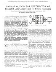
Fig. 6. Comparison of CDAC switching energy with [11] <strong>and</strong> [17] for a<br />
10-<strong>bit</strong> <strong>SAR</strong> <strong>ADC</strong>.<br />
TABLE I<br />
DAC SWITCHING ENERGY COMPARISON FOR A 10-b <strong>SAR</strong> <strong>ADC</strong><br />
Spec. [17] [18] [11] This Scheme<br />
Avg. Energy (C.Vref 2 ) 142 255.5 170 106<br />
Energy Saving 25.3 % 58.6 % 37.5 % –<br />
cycle <strong>and</strong> hence speed is not compromised. The flipping of<br />
the CDAC is done only for the first DOWN transition by<br />
making use of the symmetric structure of the CDAC, for both<br />
UP <strong>and</strong> DOWN transitions, from this node. The splitting of<br />
(<strong>MS</strong>B − 1)th capaci<strong>to</strong>r helps in implementing binary search<br />
algorithm, after flipping, without incurring extra time <strong>and</strong><br />
switching. The energy consumption during various steps for<br />
a 4-<strong>bit</strong> <strong>ADC</strong> is also compared with [11, Fig. 5]. The number<br />
in the circle represents the <strong>to</strong>tal number of unit capaci<strong>to</strong>rs<br />
connected <strong>to</strong> V ref . The relative energy costs are shown on the<br />
arrows.<br />
Fig. 6 depicts the comparison of the energy drawn from<br />
the reference for each code in a 10-<strong>bit</strong> <strong>SAR</strong> <strong>ADC</strong> in [11]<br />
<strong>and</strong> [17], <strong>and</strong> FlipDAC switching scheme. Note that the<br />
proposed switching technique achieves minima at code 511<br />
<strong>and</strong> 512 compared <strong>to</strong> maxima in [11]. This happens because<br />
code 511 <strong>and</strong> code 512 are resolved by tracking code 0 <strong>and</strong><br />
code 1023, respectively, which have no DOWN transitions.<br />
Table I compares the proposed scheme with the present stateof-the-art<br />
CDAC switching schemes for a 10-<strong>bit</strong> <strong>ADC</strong>, <strong>and</strong><br />
shows energy savings achieved by the proposed scheme over<br />
them. This scheme necessitates the use of separate sampling<br />
capaci<strong>to</strong>rs which upon investigation is found favorable in<br />
reducing the power consumption in the <strong>VGA</strong> <strong>and</strong> is explained<br />
in Section II-B.<br />
B. Ping-Pong Input Sampling<br />
Fig. 7(a) depicts the timing diagram in a conventional<br />
8-<strong>bit</strong> <strong>SAR</strong> <strong>ADC</strong>. Typically, 2-3 <strong>bit</strong> cycles or equivalent delay<br />
(T vga ) is dedicated <strong>to</strong> the tracking of the input on the CDAC<br />
(C DAC ). It is then followed by 8-<strong>bit</strong> cycles for the digitization<br />
of the sample. It dem<strong>and</strong>s large b<strong>and</strong>width (current) in the<br />
<strong>VGA</strong>. The power consumption in the <strong>VGA</strong> can be reduced<br />
by giving more time for the input tracking but it contradicts<br />
1 2 3 4 5 6 7<br />
Tracking<br />
Tvga<br />
8 <strong>bit</strong> cycles<br />
8 9 10<br />
Ts<br />
Ts<br />
Tracking odd sample <strong>and</strong><br />
Tracking even sample <strong>and</strong><br />
Digitizing even sample Digitizing odd sample<br />
Sampling<br />
Instant<br />
Sampling<br />
Instant<br />
Sampling<br />
Instant<br />
Ts<br />
(a)<br />
(b)<br />
Tref<br />
Sampling<br />
Instant<br />
Fig. 7. Input sampling in a <strong>SAR</strong> <strong>ADC</strong>. (a) Conventional sampling.<br />
(b) Ping-pong input sampling.<br />
<strong>VGA</strong><br />
Vip<br />
Vim<br />
0<br />
1<br />
1 1<br />
Cin1<br />
0 0<br />
Cin0<br />
Cin0<br />
0 0<br />
Cin1<br />
1 1<br />
1<br />
0<br />
0<br />
1<br />
Vin,cm<br />
1<br />
0<br />
Vcm<br />
clk0<br />
Ts<br />
<strong>ADC</strong>p<br />
<strong>ADC</strong>m<br />
clk1<br />
Ts<br />
<strong>ADC</strong><br />
Fig. 8. Architecture of the ping-pong input sampling scheme <strong>to</strong> relax the<br />
b<strong>and</strong>width requirement of <strong>VGA</strong> <strong>and</strong> reference buffer. V in,cm is the output<br />
common mode voltage of the <strong>VGA</strong>.<br />
with the design of the reference buffer. In this <strong>ADC</strong>, separate<br />
sampling <strong>and</strong> DAC capacitance is used <strong>to</strong> decouple the design<br />
of two blocks <strong>and</strong> employ ping-pong input sampling [14].<br />
Figs. 7(b) <strong>and</strong> 8 illustrate the sampling scheme employed<br />
in the <strong>ADC</strong>. In this scheme, inputs are sampled on capaci<strong>to</strong>rs<br />
(C in0 <strong>and</strong> C in1 ) rather than C DAC . There are two sets of<br />
sampling capaci<strong>to</strong>rs of which when one tracks the input, the<br />
other is used <strong>to</strong> digitize the previous sample. This enables<br />
the use of the complete sample period [T S in Fig. 7(b)] for<br />
the input tracking, which relaxes the b<strong>and</strong>width requirement of<br />
the <strong>VGA</strong>. It also reduces the power consumption in the<br />
reference buffer as comparatively more time is available for<br />
<strong>bit</strong> cycling. Ping-pong sampling in the <strong>ADC</strong> enables the use<br />
of two half rate clocks for even- <strong>and</strong> odd-numbered channels.<br />
It alleviates the clock requirement by 2X, over asynchronous<br />
schemes employing clocks equal <strong>to</strong> that of the sampling<br />
rate, which reduces power consumption in clock buffers.<br />
The following section quantitatively shows the advantage due<br />
<strong>to</strong> the sampling scheme. The settling mechanism is assumed<br />
<strong>to</strong> be of first order <strong>and</strong> the analysis is done for settling error<br />
of 1 LSB = V ref /2 N .