An 8-to-1 bit 1-MS/s SAR ADC With VGA and Integrated Data ...
An 8-to-1 bit 1-MS/s SAR ADC With VGA and Integrated Data ...
An 8-to-1 bit 1-MS/s SAR ADC With VGA and Integrated Data ...

You also want an ePaper? Increase the reach of your titles
YUMPU automatically turns print PDFs into web optimized ePapers that Google loves.
This article has been accepted for inclusion in a future issue of this journal. Content is final as presented, with the exception of pagination.<br />
8 IEEE TRANSACTIONS ON VERY LARGE SCALE INTEGRATION (VLSI) SYSTE<strong>MS</strong><br />
Vcm<br />
0.6<br />
DNL<br />
Even Channels<br />
Vcm<br />
Vip0<br />
Vim0<br />
Vcm<br />
S<br />
S<br />
H<br />
CS0<br />
CS1<br />
Sp<br />
Sp<br />
Hp<br />
Hp<br />
S<br />
Vincm<br />
Hp<br />
Hp<br />
Cf0<br />
−<br />
Gm<br />
+<br />
S<br />
H<br />
H<br />
0.4<br />
0.2<br />
0<br />
−0.2<br />
−0.4<br />
0 20 40 60 80 100 120 140 160 180 200 220 240 255<br />
0.4<br />
INL<br />
0.2<br />
S<br />
Sp<br />
H<br />
Hp<br />
S<br />
Cf1<br />
Vcm<br />
Vcm<br />
S<br />
Vom<br />
Vop<br />
<strong>ADC</strong><br />
0<br />
−0.2<br />
−0.4<br />
−0.6<br />
0 20 40 60 80 100 120 140 160 180 200 220 240 255<br />
H<br />
Vcm<br />
Vip1<br />
Vim1<br />
S<br />
Vcm<br />
H<br />
CS2<br />
Hp<br />
Hp<br />
CS3<br />
Odd Channels<br />
Sp<br />
Sp<br />
H<br />
Vincm<br />
H<br />
Sp<br />
Sp<br />
Cf2<br />
Gm<br />
Cf3<br />
Vcm<br />
H<br />
S<br />
S<br />
H<br />
clk=Fs/2<br />
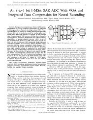
Fig. 15. Architecture of each of the <strong>VGA</strong> stage. For better matching, OTA<br />
is shared between even- <strong>and</strong> odd-numbered channel.<br />
Fig. 17. Measured DNL <strong>and</strong> INL plots. Y -axisisinLSB<strong>and</strong>X-axis is the<br />
output digital code.<br />
50<br />
SNDR (dB)<br />
49<br />
48<br />
47<br />
46<br />
45<br />
44<br />
43<br />
42<br />
0 0.1 0.2 0.3 0.4 0.5<br />
Input Frequency (MHz)<br />
Fig. 18.<br />
Measured SNDR versus F in for −1 dBFS input at 1 <strong>MS</strong>/s speed.<br />
Fig. 16. Die pho<strong>to</strong>graph of the chip designed in UMC 0.13-μm CMOS<br />
technology.<br />
(fixed) + 80 fF (programmable in four steps). Voltage gains<br />
that can be achieved with one <strong>VGA</strong> stage are 2.5, 3.75,<br />
5, <strong>and</strong> 7.5 V/V. The programmable voltage gain range is<br />
2.5–56.25 V/V in eight steps. We have also designed<br />
an on-chip voltage reference buffer for the <strong>ADC</strong>. The<br />
OTA designed for the reference buffer is a two-stage<br />
trans-conductance amplifier consuming 4 μA <strong>and</strong> is load<br />
compensated.<br />
IV. EXPERIMENTAL RESULTS<br />
A. <strong>ADC</strong> Characterization<br />
Fig. 16 shows a die pho<strong>to</strong> of the chip fabricated in UMC<br />
0.13-μm CMOS technology. The <strong>ADC</strong> occupies an area of<br />
390 μm × 420 μm. The charge redistribution DAC employs<br />
cus<strong>to</strong>m made unit capaci<strong>to</strong>r ∼ 15 fF using metal-oxide-metal<br />
(MOM) technology with six metal layers. This value of the<br />
unit capacitance is larger than the required unit capacitance<br />
size for an 8-<strong>bit</strong> <strong>ADC</strong> with σ C /C 0 = 0.5%. The <strong>to</strong>tal DAC<br />
capacitance is 3.84 pF. The full scale range (FSR) of the <strong>ADC</strong><br />
is 1 V pp differential.<br />
The maximum measured INL <strong>and</strong> DNL (Fig. 17) are found<br />
<strong>to</strong> be 0.6 LSB/−0.7LSB<strong>and</strong>0.26LSB/−0.67 LSB. These<br />
are at 0.25 FSR <strong>and</strong> 0.75 FSR due <strong>to</strong> a mismatch between the<br />
two paths (Fig. 12) meant for interchanging two DAC inputs <strong>to</strong><br />
the preamplifier once they are flipped. Fig. 19 shows 16 384<br />
point FFT of the <strong>ADC</strong> output for −1 dBFS input at F in =<br />
62.439 kHz. Fig. 18 presents the measured signal-<strong>to</strong>-noise<strong>and</strong>-dis<strong>to</strong>rtion<br />
ratio (SNDR) for different input frequencies at<br />
−1 dBFS input. The <strong>ADC</strong> achieves a SNDR of 48.1 dB for a<br />
near Nyquist input (499.939 kHz), which translates <strong>to</strong> effective<br />
number of <strong>bit</strong>s (ENOB) of 7.7 <strong>bit</strong>s.<br />
The <strong>ADC</strong> consumes <strong>to</strong>tal power of 8.8 μW with V DD = 1V<br />
at 8-<strong>bit</strong> setting. Based on parasitic extracted simulations,