An 8-to-1 bit 1-MS/s SAR ADC With VGA and Integrated Data ...
An 8-to-1 bit 1-MS/s SAR ADC With VGA and Integrated Data ...
An 8-to-1 bit 1-MS/s SAR ADC With VGA and Integrated Data ...

You also want an ePaper? Increase the reach of your titles
YUMPU automatically turns print PDFs into web optimized ePapers that Google loves.
This article has been accepted for inclusion in a future issue of this journal. Content is final as presented, with the exception of pagination.<br />
2 IEEE TRANSACTIONS ON VERY LARGE SCALE INTEGRATION (VLSI) SYSTE<strong>MS</strong><br />
<strong>VGA</strong> REFBFR<br />
REFP<br />
Vcm<br />
REFM<br />
Vip0<br />
Vim0<br />
Vip1<br />
Vim1<br />
CDAC<br />
Vinp<br />
Vdacp<br />
Vdacm<br />
Vinm<br />
+<br />
-<br />
+ Av<br />
-<br />
compara<strong>to</strong>r<br />
Vop<br />
Flip<br />
Vip<br />
Vim<br />
clk=Fs/2<br />
Switch Control<br />
Pingpong<br />
Sampling<br />
Sth<br />
Threshold<br />
N[2:0]<br />
<strong>and</strong> Noise noise<br />
Sth<br />
Estimation<br />
Cin0<br />
Cin1<br />
DR<br />
Vom<br />
LATCH<br />
outp<br />
outm<br />
<strong>Data</strong> Register<br />
STB<br />
clk<br />
Asynchronous<br />
<strong>SAR</strong> Logic<br />
Digital Output<br />
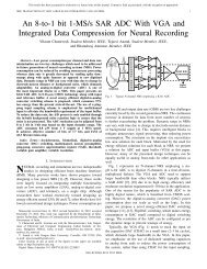
Fig. 2. Block diagram of the proposed <strong>SAR</strong> <strong>ADC</strong> with an on-chip voltage<br />
reference buffer (REFBFR).<br />
We also recommend employing a ping-pong input sampling<br />
architecture [14] <strong>to</strong> alleviate the b<strong>and</strong>width requirement of the<br />
<strong>VGA</strong>. It is explained in more detail in Section II-B. The amplitude<br />
of the maximum detectable signal varies with neuronelectrode<br />
distance <strong>and</strong> probe impedance, which is frequency<br />
dependent. A fixed gain in NRS will either under-utilize the<br />
<strong>ADC</strong> dynamic range or causes clipping of the peaks. Hence,<br />
we emphasize a large programmable range in voltage gain of<br />
the <strong>VGA</strong>. The designed <strong>VGA</strong> has voltage gain programmable<br />
from 8 <strong>to</strong> 35 dB in eight steps.<br />
NRS generate tremendous amount of data due <strong>to</strong> chronic<br />
recording from a large number of neurons [3]. The transmission<br />
of this large amount of data through a wireless link<br />
poses serious threat <strong>to</strong> the scalability <strong>and</strong> power efficiency<br />
of BMI. Spike feature extraction [1] <strong>and</strong> simple thresholding<br />
[2] are two popular ways through which researchers have<br />
tried <strong>to</strong> reduce output data rate. However, the former needs<br />
extra hardware <strong>and</strong> power whereas the latter can cause loss<br />
of information for spike sorting. The present low ODR NRSs<br />
typically need an extra spike detection block, e.g., one DAC<br />
per channel [2], which consumes large area. In this paper,<br />
we merge spike detection logic in<strong>to</strong> the <strong>ADC</strong>, reusing the<br />
CDAC in it. This scheme not only mitigates the processing of<br />
the background noise <strong>to</strong> reduce the ODR but also preserves<br />
important spike features, which are required for the spike<br />
sorting [15]. It also helps in reducing power consumption <strong>and</strong><br />
area of NRS.<br />
This paper is organized as follows. Section II presents the<br />
architecture of the <strong>ADC</strong>, ping-pong input sampling scheme <strong>to</strong><br />
relax <strong>VGA</strong> specification <strong>and</strong> activity-dependent A/D scheme<br />
<strong>to</strong> reduce ODR. Section II also explains the energy efficient<br />
DAC switching technique, FlipDAC. Section III discusses the<br />
circuit implementation of various blocks. Section IV presents<br />
the measured results from a chip fabricated in UMC 0.13-μm<br />
CMOS technology. Section V concludes this paper.<br />
II. <strong>ADC</strong> ARCHITECTURE<br />
The block diagram of the proposed <strong>SAR</strong> <strong>ADC</strong> is shown in<br />
Fig. 2. Fully differential input <strong>and</strong> reference voltages are used.<br />
The reference DAC <strong>and</strong> sampling capaci<strong>to</strong>rs are segregated<br />
<strong>to</strong> gain advantages explained in Section II-B. A four-input<br />
preamplifier is used in the compara<strong>to</strong>r <strong>to</strong> mitigate the effect of<br />
kickback noise on sampling capaci<strong>to</strong>rs (C in0,1 ). A master clock<br />
NEXT<br />
Vcm<br />
2C C C<br />
Vcm<br />
2C C C<br />
Vcm<br />
E=0<br />
+<br />
−<br />
Vdac=0<br />
2C<br />
Vcm<br />
2C<br />
V<br />
Vcm+V/4<br />
C C<br />
+<br />
C C<br />
Vcm-V/4<br />
E=0.5<br />
(a)<br />
−<br />
Vdac=V/2<br />
V<br />
2C<br />
Vcm<br />
Vcm+V/4<br />
2C C C<br />
C C<br />
+<br />
+<br />
Vcm<br />
Vcm<br />
−<br />
−<br />
2C C C Vdac=0<br />
C C Vdac=V/2<br />
Vcm<br />
Vcm-V/4<br />
2C<br />
E=0 E=0.5<br />
(b)<br />
UP<br />
DOWN<br />
UP<br />
DOWN<br />
2C C Vdac=3V/4<br />
Vcm+3V/8 C<br />
+<br />
Vcm<br />
−<br />
Vcm-3V/8 C<br />
2C C<br />
E=1/8<br />
2C C Vdac=V/4<br />
Vcm+V/8 C<br />
+<br />
Vcm<br />
−<br />
Vcm-V/8 C<br />
2C C<br />
2C C<br />
Vdac=3V/4<br />
Vcm+3V/8 C<br />
+<br />
Vcm<br />
−<br />
Vcm-3V/8 C<br />
2C C<br />
Vcm<br />
2C<br />
2C<br />
V<br />
V<br />
V<br />
C Vcm-V/8<br />
C<br />
+ -Vdac=V/4<br />
V<br />
C<br />
V<br />
V<br />
V<br />
E=5/8<br />
E=1/8<br />
−<br />
C FlipDac<br />
Vcm+V/8<br />
E=1/8<br />
Fig. 3. (a) DAC switching in a 3-<strong>bit</strong> <strong>SAR</strong> <strong>ADC</strong> [11]. (b) FlipDAC switching.<br />
In the figure, V = 2·V cm = V ref <strong>and</strong> the unit of energy consumption is C.Vref 2 .<br />
Vip-Vin<br />
purge<br />
FlipDac<br />
Vdacp-Vdacm<br />
1 1 1 0 1 0 0 1<br />
Flip<br />
Strobe<br />
Vref-(Vip-Vin)<br />
Vdacm-Vdacp<br />
sign b2 b1 b0 sign b2 b1 b0<br />
Fig. 4. Input digitization through the proposed FlipDAC switching technique.<br />
In the second case, output 1001 is resolved indirectly by tracking 1110 by<br />
V dacp − V dacm .<br />
of only half the sampling speed is used due <strong>to</strong> the ping-pong<br />
input sampling architecture. It reduces the power consumption<br />
in clock buffers by 2× <strong>and</strong> decreases the <strong>to</strong>tal system power<br />
consumption. To reduce output data rate, the detection of the<br />
neural spikes is achieved using spike threshold S TH ,which<br />
is calculated based on the background noise <strong>and</strong> is s<strong>to</strong>red in<br />
registers. This is explained more in Section II-C. The dynamic<br />
range (DR) decides the resolution setting (N) of the <strong>ADC</strong>. <strong>An</strong><br />
on-chip voltage reference buffer is implemented <strong>to</strong> provide<br />
clean <strong>and</strong> stable voltage reference <strong>to</strong> the <strong>ADC</strong>.<br />
A. FlipDAC Switching<br />
Of late, there has been a lot of interest in energy efficient<br />
DAC switching techniques for CDAC [11]–[13]. It has been<br />
shown that the DOWN transitions take more energy than