Characterization of vacancy-type defects in silicon using deep level ...
Characterization of vacancy-type defects in silicon using deep level ...
Characterization of vacancy-type defects in silicon using deep level ...

Create successful ePaper yourself
Turn your PDF publications into a flip-book with our unique Google optimized e-Paper software.
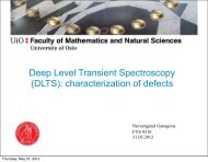
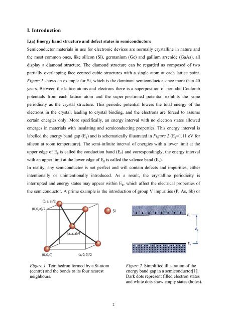
I. IntroductionI.(a) Energy band structure and defect states <strong>in</strong> semiconductorsSemiconductor materials <strong>in</strong> use for electronic devices are normally crystall<strong>in</strong>e <strong>in</strong> nature andthe most common ones, like <strong>silicon</strong> (Si), germanium (Ge) and gallium arsenide (GaAs), alldisplay a diamond structure. The diamond structure can be regarded as composed <strong>of</strong> twopartially overlapp<strong>in</strong>g face centred cubic structures with a s<strong>in</strong>gle atom at each lattice po<strong>in</strong>t.Figure 1 shows an example for Si, which is the dom<strong>in</strong>ant semiconductor s<strong>in</strong>ce more than 40years. Between the lattice atoms and electrons there is a superposition <strong>of</strong> periodic Coulombpotentials from each lattice atom and the super-positioned potential exhibits the sameperiodicity as the crystal structure. This periodic potential lowers the total energy <strong>of</strong> theelectrons <strong>in</strong> the crystal, lead<strong>in</strong>g to crystal b<strong>in</strong>d<strong>in</strong>g, and the electrons are forced to assumecerta<strong>in</strong> energies only. More specifically, an energy <strong>in</strong>terval with no electron states allowedemerges <strong>in</strong> materials with <strong>in</strong>sulat<strong>in</strong>g and semiconduct<strong>in</strong>g properties. This energy <strong>in</strong>terval islabelled the energy band gap (E g ) and is schematically illustrated <strong>in</strong> Figure 2 (E g ≈1.11 eV for<strong>silicon</strong> at room temperature). The semi-<strong>in</strong>f<strong>in</strong>ite <strong>in</strong>terval <strong>of</strong> energies with a lower limit at theupper edge <strong>of</strong> E g is called the conduction band (E c ) and correspond<strong>in</strong>gly, the energy <strong>in</strong>tervalwith an upper limit at the lower edge <strong>of</strong> E g is called the valence band (E v ).In reality, any semiconductor is not perfect and will conta<strong>in</strong> <strong>defects</strong> and impurities, either<strong>in</strong>tentionally or un<strong>in</strong>tentionally <strong>in</strong>troduced. As a result, the crystall<strong>in</strong>e periodicity is<strong>in</strong>terrupted and energy states may appear with<strong>in</strong> E g , which affect the electrical properties <strong>of</strong>the semiconductor. A prime example is the <strong>in</strong>troduction <strong>of</strong> group V impurities (P, As, Sb) orFigure 1. Tetrahedron formed by a Si-atom(centre) and the bonds to its four nearestneighbours.Figure 2. Simplified illustration <strong>of</strong> theenergy band gap <strong>in</strong> a semiconductor[1].Dark dots represent filled electron statesand white dots show empty states (holes).2