Characterization of vacancy-type defects in silicon using deep level ...
Characterization of vacancy-type defects in silicon using deep level ...
Characterization of vacancy-type defects in silicon using deep level ...

Create successful ePaper yourself
Turn your PDF publications into a flip-book with our unique Google optimized e-Paper software.
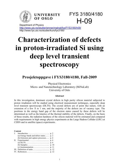
Department <strong>of</strong> Physicshttp://www.uio.no/studier/emner/matnat/fys/FYS3180/h09/http://www.fys.uio.no/studier/kurs/fys3180/FYS 3180/4180H-09<strong>Characterization</strong> <strong>of</strong> <strong>defects</strong><strong>in</strong> proton-irradiated Si us<strong>in</strong>g<strong>deep</strong> <strong>level</strong> transientspectroscopyProsjektoppgave i FYS3180/4180, Fall-2009Physical ElectronicsMicro- and Nanotechnology Laboratory (MiNaLab)University <strong>of</strong> OsloAbstractIn this <strong>in</strong>vestigation, dom<strong>in</strong>ant crystal <strong>defects</strong> <strong>in</strong> high purity <strong>silicon</strong> material subjected toproton irradiation will be studied us<strong>in</strong>g electrical measurement techniques, especially <strong>deep</strong><strong>level</strong> transient spectroscopy (DLTS). The crystal <strong>defects</strong> are <strong>of</strong> po<strong>in</strong>t like nature, with anextension <strong>of</strong> a few Å to 1 nm, and the majority <strong>of</strong> the <strong>defects</strong> are <strong>of</strong> <strong>vacancy</strong> <strong>type</strong>. Thepositions <strong>in</strong> the energy band gap <strong>of</strong> the electron states caused by these <strong>defects</strong> will bedeterm<strong>in</strong>ed as well as the k<strong>in</strong>etics <strong>of</strong> the thermal stability <strong>of</strong> the <strong>defects</strong>. F<strong>in</strong>ally, on the basis<strong>of</strong> these results, the radiation hardness <strong>of</strong> the <strong>silicon</strong> material will be estimated and comparedwith requirements <strong>in</strong> high energy physics experiments at the Large Hadron Collider (LHC) atCERN and <strong>in</strong> satellite (space) experiments.ContentI. Introduction…………………………... p. 2(a) Energy bands and defect states…… p. 2(b) Emission and capture processes….. p. 4II. Experimental…………......................... p. 6(a) DLTS……………………………... p. 6(b) Samples…………………………... p. 10(c) Instrumentation………………….... p. 11III. Def<strong>in</strong>ition <strong>of</strong> tasks……......................... p. 12IV. References……………......................... p. 121
I. IntroductionI.(a) Energy band structure and defect states <strong>in</strong> semiconductorsSemiconductor materials <strong>in</strong> use for electronic devices are normally crystall<strong>in</strong>e <strong>in</strong> nature andthe most common ones, like <strong>silicon</strong> (Si), germanium (Ge) and gallium arsenide (GaAs), alldisplay a diamond structure. The diamond structure can be regarded as composed <strong>of</strong> twopartially overlapp<strong>in</strong>g face centred cubic structures with a s<strong>in</strong>gle atom at each lattice po<strong>in</strong>t.Figure 1 shows an example for Si, which is the dom<strong>in</strong>ant semiconductor s<strong>in</strong>ce more than 40years. Between the lattice atoms and electrons there is a superposition <strong>of</strong> periodic Coulombpotentials from each lattice atom and the super-positioned potential exhibits the sameperiodicity as the crystal structure. This periodic potential lowers the total energy <strong>of</strong> theelectrons <strong>in</strong> the crystal, lead<strong>in</strong>g to crystal b<strong>in</strong>d<strong>in</strong>g, and the electrons are forced to assumecerta<strong>in</strong> energies only. More specifically, an energy <strong>in</strong>terval with no electron states allowedemerges <strong>in</strong> materials with <strong>in</strong>sulat<strong>in</strong>g and semiconduct<strong>in</strong>g properties. This energy <strong>in</strong>terval islabelled the energy band gap (E g ) and is schematically illustrated <strong>in</strong> Figure 2 (E g ≈1.11 eV for<strong>silicon</strong> at room temperature). The semi-<strong>in</strong>f<strong>in</strong>ite <strong>in</strong>terval <strong>of</strong> energies with a lower limit at theupper edge <strong>of</strong> E g is called the conduction band (E c ) and correspond<strong>in</strong>gly, the energy <strong>in</strong>tervalwith an upper limit at the lower edge <strong>of</strong> E g is called the valence band (E v ).In reality, any semiconductor is not perfect and will conta<strong>in</strong> <strong>defects</strong> and impurities, either<strong>in</strong>tentionally or un<strong>in</strong>tentionally <strong>in</strong>troduced. As a result, the crystall<strong>in</strong>e periodicity is<strong>in</strong>terrupted and energy states may appear with<strong>in</strong> E g , which affect the electrical properties <strong>of</strong>the semiconductor. A prime example is the <strong>in</strong>troduction <strong>of</strong> group V impurities (P, As, Sb) orFigure 1. Tetrahedron formed by a Si-atom(centre) and the bonds to its four nearestneighbours.Figure 2. Simplified illustration <strong>of</strong> theenergy band gap <strong>in</strong> a semiconductor[1].Dark dots represent filled electron statesand white dots show empty states (holes).2
group III impurities (B, Al, Ga, In) on substitutional lattice sites <strong>in</strong> the <strong>silicon</strong> structure (socalleddop<strong>in</strong>g). The former ones will give rise to shallow electron states <strong>in</strong> E g with respect toE c and readily become positively ionized by thermal excitation <strong>of</strong> electrons to the almostempty conduction band (n-<strong>type</strong> dop<strong>in</strong>g). Correspond<strong>in</strong>gly, the group III elements will causeshallow electron states <strong>in</strong> E g with respect to E v and readily become negatively ionized bythermal excitation <strong>of</strong> electrons from the almost fully occupied valence band (p-<strong>type</strong> dop<strong>in</strong>g).Consequently, the electrical conductivity <strong>of</strong> the Si material can be drastically changed, eitherby current transport via the almost free electrons <strong>in</strong> the conduction band (n-<strong>type</strong> conductivity)or via the valence electrons ‘jump<strong>in</strong>g’ to nearby empty states, so-called holes (p-<strong>type</strong>conductivity)[1]. In addition, native (<strong>in</strong>tr<strong>in</strong>sic) crystall<strong>in</strong>e <strong>defects</strong> and un<strong>in</strong>tentionally<strong>in</strong>troduced residual impurities can appear <strong>in</strong> the material and some fundamental examples likevacancies and self-<strong>in</strong>terstitials are schematically illustrated <strong>in</strong> Figure 3.In <strong>silicon</strong>, the ma<strong>in</strong> residual impurities are oxygen, carbon and hydrogen[2]. Especially,oxygen can occur with high concentrations <strong>in</strong> as-grown s<strong>in</strong>gle crystall<strong>in</strong>e <strong>silicon</strong> material(~1x10 18 cm -3 , compared to the atomic density <strong>of</strong> ~5x10 22 cm -3 ) and these oxygen atomsoccupy normally a bond-centred <strong>in</strong>terstitial configuration (O i ), as illustrated <strong>in</strong> some detail byFigure 4(a). The O i atoms do not give rise to any energy state <strong>in</strong> E g but they are likely tocapture monovacancies (V’s) <strong>in</strong> order to release the crystal stra<strong>in</strong> associated with the O iconfiguration. The result<strong>in</strong>g defect formed is shown <strong>in</strong> Figure 4(b) and is labelled the<strong>vacancy</strong>-oxygen (VO) centre[3]. The VO centre conta<strong>in</strong>s two dangl<strong>in</strong>g bonds from the twounsaturated Si atoms and an electron energy state appears at ~0.18 eV below E c . Anotherprom<strong>in</strong>ent defect <strong>in</strong> <strong>silicon</strong> is the di<strong>vacancy</strong> centre (V 2 )[4] which consists <strong>of</strong> two V’s <strong>in</strong>nearest neighbour lattice positions, as displayed <strong>in</strong> Figure 4(c). The V 2 centre appears <strong>in</strong>particular after a <strong>silicon</strong> material has been exposed to irradiation with energetic particles, likeprotons and electrons <strong>in</strong> high energy physics experiments or <strong>in</strong> the Van Allen radiation belt,Figure 3. Illustration <strong>of</strong> fundamentalpo<strong>in</strong>t <strong>defects</strong>; <strong>vacancy</strong> (top right), self<strong>in</strong>terstitial(bottom right), substitutionalimpurity (top left) and <strong>in</strong>terstitialimpurity (bottom left). Open circlesillustrate crystal host atoms and filleddark circles <strong>in</strong>dicate impurity atoms.3
Figure 4. Visualization <strong>of</strong> the atomicstructure <strong>of</strong> the O i (a), VO (b) and V 2 (c)<strong>defects</strong>.Electron and charge states for V 2Figure 5. Illustration <strong>of</strong> electronstates and charge states for theV 2 centre <strong>in</strong> <strong>silicon</strong>.E C2--0.23 eV0.43 eV0E V+0.20 eVand it causes three different electron states <strong>in</strong> E g correspond<strong>in</strong>g to four charge states <strong>of</strong> V 2 (+,0, -1, -2), as depicted <strong>in</strong> Figure 5.I.(b) Emission and capture <strong>of</strong> electrons/holes by energy states <strong>in</strong> the band gapLet us consider an electron state at an energy E T below E c and with a concentration <strong>of</strong> N T .Figure 6(a) shows the total ‘traffic’ <strong>of</strong> electrons and holes to and from this state. The rate <strong>of</strong>emission <strong>of</strong> an electron to E c and a hole to E v are denoted by e n and e p , respectively. The rate<strong>of</strong> capture <strong>of</strong> an electron from E c or a hole from E v are nc n and pc p , respectively, where c n andc p are the so-called capture coefficients, and n and p are the concentrations <strong>of</strong> electrons <strong>in</strong> theconduction band and holes <strong>in</strong> the valence band, respectively.4
Figure 6. The total ‘traffic’ <strong>of</strong>charge carriers to and from a state isshown <strong>in</strong> (a). The special case <strong>of</strong>recomb<strong>in</strong>ation is given <strong>in</strong> (b),trapp<strong>in</strong>g and emission <strong>in</strong> (c), andgeneration <strong>in</strong> (d).}E TThree typical situations can be identified; first, as shown <strong>in</strong> Figure 6(b), a state may act as arecomb<strong>in</strong>ation centre for pairs <strong>of</strong> electrons and holes. Second, as shown <strong>in</strong> Figure 6(c), a statecan act as a trap, and trapp<strong>in</strong>g and emission <strong>of</strong> electrons (or holes) are the dom<strong>in</strong>at<strong>in</strong>gprocesses. Third, as shown <strong>in</strong> Figure 6(d), a state can act as a generation centre for pairs <strong>of</strong>electrons and holes.Accord<strong>in</strong>g to Shockley and Read[5], the capture coefficient for a state can be expressed as:c n(p) = σ n(p) v thwhere σ n(p) is the capture cross section for electrons (holes) and v th is the thermal velocity,v th = (3kT/m* n(p) ) ½with m* n(p) as the effective mass for electrons (holes), T as the absolute temperature, and k asBoltzmann’s constant.For the emission rate, the follow<strong>in</strong>g relation holds[5]:e n(p) (T) = v th σ n(p) N C(V) exp(-E T /kT) (1)where N C(V) is the effective density <strong>of</strong> states <strong>in</strong> the conduction (valence) band.5
II. ExperimentalII.(a) Sample analysis by <strong>deep</strong> <strong>level</strong> transient spectroscopy (DLTS)DLTS is the ma<strong>in</strong> technique to be used for the sample analysis, and <strong>in</strong> this section a brief<strong>in</strong>troduction to the basic pr<strong>in</strong>ciples <strong>of</strong> DLTS is given. The technique was first <strong>in</strong>troduced byLang <strong>in</strong> 1974[6] and from DLTS one can obta<strong>in</strong> <strong>in</strong>formation about energy positions <strong>of</strong> states<strong>in</strong> the band gap, capture cross sections for electrons and holes, average concentration <strong>of</strong>energy states (<strong>defects</strong>) as well as concentration-versus-depth pr<strong>of</strong>iles <strong>of</strong> the states. Inparticular, a hallmark <strong>of</strong> DLTS is a very high sensitivity reach<strong>in</strong>g detection limits on the order<strong>of</strong> 10 -5 relative to the dop<strong>in</strong>g concentration.DLTS requires a good rectify<strong>in</strong>g junction <strong>in</strong> a semiconductor material, either a pn-junction ora Schottky barrier junction, and it is based on measurements <strong>of</strong> the junction capacitance. Thebasic structure <strong>of</strong> a pn-junction is given <strong>in</strong> Figure 7, and with the junction is associated adepletion region, W , which is depleted <strong>of</strong> free charge carriers (electrons and holes). As aresult <strong>of</strong> W , a capacitance,C r, builds up at the junction and is given byεA2εVr1 1C r= with W = ( + )Wq N Nadwhere ε is the permittivity (dielectric constant) <strong>of</strong> the material, A is the diode area,V ris totalbias over the junction, q is the elementary charge,N ais the acceptor dop<strong>in</strong>g concentrationandN dis the donor concentration.normally used for DLTSmeasuremFigure 7. Schematics <strong>of</strong>a pn-junction show<strong>in</strong>g−+the ionized N aand N ddopants <strong>in</strong> the p- and n-regions, respectively.ents, and foWr adenotes the depletionregion.In practice, an asymmetrically doped junction, like p + n ( N >> N ) or a Schottky junction, isadnormally used for DLTS measurements and for a p + n-junctionC ris simplified toCr=A εqN2 Vrd.6
In accordance with section I.(b), let us consider an electron state <strong>in</strong> the upper half <strong>of</strong> E g with aposition <strong>of</strong> E T below E c , as shown <strong>in</strong> Figure 6(c), and a concentration <strong>of</strong>. In DLTS, thecapacitance is measured dur<strong>in</strong>g puls<strong>in</strong>g <strong>of</strong> the junction voltage and a measurement sequence isillustrated <strong>in</strong> Figure 8. In Figure 8(a), the junction is kept at reverse bias and the electron stateis empty <strong>in</strong> the depletion region. In Figure 8(b), a voltage pulse is applied and the reverse biasis reduced; as a result, the width <strong>of</strong> W decreases and the electron state can capture electronsprovided that the duration <strong>of</strong> the pulse is sufficiently long. In Figure 8(c), the voltageN T(a)(b)(c)Figure 8. DLTS voltage pulsesequence for a p + n junction.Electron occupation <strong>of</strong> stateE T and depletion layer widthare <strong>in</strong>dicated correspond<strong>in</strong>g to(a) before, (b) dur<strong>in</strong>g and (c)after the pulse. In (c), also theevolution <strong>of</strong> the capacitanceas function <strong>of</strong> time after thepulse removal is <strong>in</strong>dicated fordifferent temperatures.pulse is removed andV rreturns to its value <strong>in</strong> Figure 8(a). After remov<strong>in</strong>g the pulse <strong>in</strong>Figure 8(c), the effective dop<strong>in</strong>g concentration,effNd, <strong>in</strong> W is given bywhereNeffd= Nd− nT(t)The quantity(t)n T(t) = N Texp(-e n t).represents the concentration <strong>of</strong> filled electron states as a function <strong>of</strong> time,n Tt, after the pulse removal. The expression above for (t)can be derived from Shockley-Read-Hall statistics[5] and shows that the empty<strong>in</strong>g <strong>of</strong> the electron states is a thermallyactivated process with a rate constant equal to e n (given by Equation (1)) and an exponentialtime dependence.n T7
Hence, the capacitance after remov<strong>in</strong>g the pulse becomesC (t) =AεqN2Veffdr= Aεq(Nd− n2VrT( t))and assum<strong>in</strong>g N
In reality, the procedure outl<strong>in</strong>ed <strong>in</strong> Figure 9 for extract<strong>in</strong>g the DLTS signal is rather sensitiveto noise <strong>in</strong> the capacitance measurements and <strong>in</strong>stead, a sampl<strong>in</strong>g (weight<strong>in</strong>g) function, w(t) ,<strong>of</strong> the <strong>type</strong> shown <strong>in</strong> Figure 10 is frequently used. This sampl<strong>in</strong>g function is <strong>of</strong> lock-<strong>in</strong> <strong>type</strong>and the DLTS signal, S(t i ), is deduced accord<strong>in</strong>g toS(t i ) =1tit + td∫tdiΔC(t)w(t)dtwhere t d is a delay time <strong>of</strong> the capacitance meter. For t d
II.(b) Samples to be studiedAll the samples to be used <strong>in</strong> this study are cut from a <strong>silicon</strong> wafer hav<strong>in</strong>g a highly n-doped(n + ) substrate with a lightly n-doped (n - ) epitaxial layer grown by chemical vapour depositionat ITME[7], see the schematic <strong>in</strong> Figure 11(a). The wafers were subsequently processed bySINTEF/MiNaLab <strong>in</strong>to pads <strong>of</strong> p + -n - -n + diodes. The p + -layer was realized by ion implantation<strong>of</strong> boron. The thickness <strong>of</strong> the epitaxial n - -layer is ~20 µm and the dop<strong>in</strong>g concentration, ,<strong>in</strong> the layer is about 3x10 13 cm -3 .After process<strong>in</strong>g, rectangular samples with a size <strong>of</strong> about 2x2 mm 2 were cut form the wafers,and a photo <strong>of</strong> the processed and diced wafer is shown <strong>in</strong> Figure 11(b).F<strong>in</strong>ally, the samples were irradiated with 1.5 MeV protons at room temperature to dosesbetween 5x10 9 and 6x10 10 H + /cm 2 . The irradiations were undertaken at UiO/MiNaLab and thesamples have then been stored <strong>in</strong> a freezer at -20 °C.N d(a)(b)Figure 11. In (a), a schematic visualization <strong>of</strong> the p + -n - -n + samples is given. The front contactis the middle square, isolated by dark ditches <strong>of</strong> <strong>silicon</strong> dioxide (SiO 2 ). The thickness <strong>of</strong> theepitaxial layer is about 20 µm with N ≈3x10 13 cm -3 d. The dimensions <strong>in</strong> (a) are not to scale.In (b), a photograph <strong>of</strong> a processed and diced wafer (∅ = 150 mm) is shown. The p + -n - -n +samples can be seen as small (2 mm) 2 squares located <strong>in</strong> the areas that are covered withalum<strong>in</strong>ium (grey). The rest <strong>of</strong> the structures on the wafer are irrelevant for this <strong>in</strong>vestigation.10
II.(c) Instrumentation for the measurementsThe experimental setup to be used is designed for electrical measurements <strong>in</strong> the temperaturerange from 77 K (LN 2 ) to 400 K. The measurements <strong>in</strong>clude capacitance versus voltage andcurrent versus voltage and spectroscopic techniques like DLTS,. A block diagram <strong>of</strong> thecomponents <strong>in</strong> the setup and their <strong>in</strong>terconnections is depicted <strong>in</strong> Figure 12 together with aphotograph <strong>of</strong> the sample cryostat. A core part <strong>of</strong> the setup is the capacitance meter(HP4280A) which enables record<strong>in</strong>g <strong>of</strong> capacitance transients, Δ C(t), with a sampl<strong>in</strong>g rate <strong>of</strong>1 MHz.Figure 12. Block diagram <strong>of</strong> the DLTS setup to be used <strong>in</strong> this study. The photograph showsthe sample cryostat and the LN 2 Dewar.11
III. Def<strong>in</strong>ition <strong>of</strong> tasks• Determ<strong>in</strong>e the energy position and electron capture cross section <strong>of</strong> the dom<strong>in</strong>ant electronstates <strong>in</strong> the energy band gap <strong>of</strong> proton-irradiated high purity epitaxial <strong>silicon</strong> (n-<strong>type</strong>)• Determ<strong>in</strong>e the concentration and generation rate <strong>of</strong> the dom<strong>in</strong>ant electron states as afunction <strong>of</strong> proton dose• On the basis <strong>of</strong> comparison with literature data, identify the orig<strong>in</strong> <strong>of</strong> the dom<strong>in</strong>antelectron states• Perform isothermal anneal<strong>in</strong>g studies to determ<strong>in</strong>e the thermal stability and anneal<strong>in</strong>gk<strong>in</strong>etics <strong>of</strong> the dom<strong>in</strong>ant electron states• Conclude about the radiation hardness <strong>of</strong> the <strong>in</strong>vestigated samples (devices/detectors) andpossibly predict their lifetime <strong>in</strong> (i) the Large Hadron Collider (LHC) at CERN and (ii) asatellite exposed to the Van Allen radiation belt.IV. References[1] B.G. Streetman and S. Banerjee, Solid State Electronic Devices, Prentice HallInternational Inc., 6 th edition (2006).[2] See for example, M. Mikelsen, Thermal evolution <strong>of</strong> irradiation <strong>in</strong>duced <strong>defects</strong> <strong>in</strong> Siliconand Silicon Carbide, PhD thesis, University <strong>of</strong> Oslo (2007), and references there<strong>in</strong>.[3] J.W. Corbett, G.D. Watk<strong>in</strong>s, R.M. Chrenko and R.S. McDonald, Phys. Rev. 121, 1015(1961); G.D. Watk<strong>in</strong>s and J.W. Corbett, Phys. Rev. 121, 1001 (1961).[4] J.W. Corbett and G.D. Watk<strong>in</strong>s, Phys. Rev. Lett. 7, 314 (1961); G.D. Watk<strong>in</strong>s and J.W.Corbett, Phys. Rev. 138, A543 (1965).[5] W. Shockley and W.T. Read, Phys. Rev 87, 835 (1952).[6] D.V. Lang, J. Appl. Phys. 45, 3023 (1974).[7] Institute <strong>of</strong> Electronic Materials Technology (ITME), Warszaw, Poland.12