Characterization of vacancy-type defects in silicon using deep level ...
Characterization of vacancy-type defects in silicon using deep level ...
Characterization of vacancy-type defects in silicon using deep level ...

Create successful ePaper yourself
Turn your PDF publications into a flip-book with our unique Google optimized e-Paper software.
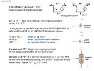
II. ExperimentalII.(a) Sample analysis by <strong>deep</strong> <strong>level</strong> transient spectroscopy (DLTS)DLTS is the ma<strong>in</strong> technique to be used for the sample analysis, and <strong>in</strong> this section a brief<strong>in</strong>troduction to the basic pr<strong>in</strong>ciples <strong>of</strong> DLTS is given. The technique was first <strong>in</strong>troduced byLang <strong>in</strong> 1974[6] and from DLTS one can obta<strong>in</strong> <strong>in</strong>formation about energy positions <strong>of</strong> states<strong>in</strong> the band gap, capture cross sections for electrons and holes, average concentration <strong>of</strong>energy states (<strong>defects</strong>) as well as concentration-versus-depth pr<strong>of</strong>iles <strong>of</strong> the states. Inparticular, a hallmark <strong>of</strong> DLTS is a very high sensitivity reach<strong>in</strong>g detection limits on the order<strong>of</strong> 10 -5 relative to the dop<strong>in</strong>g concentration.DLTS requires a good rectify<strong>in</strong>g junction <strong>in</strong> a semiconductor material, either a pn-junction ora Schottky barrier junction, and it is based on measurements <strong>of</strong> the junction capacitance. Thebasic structure <strong>of</strong> a pn-junction is given <strong>in</strong> Figure 7, and with the junction is associated adepletion region, W , which is depleted <strong>of</strong> free charge carriers (electrons and holes). As aresult <strong>of</strong> W , a capacitance,C r, builds up at the junction and is given byεA2εVr1 1C r= with W = ( + )Wq N Nadwhere ε is the permittivity (dielectric constant) <strong>of</strong> the material, A is the diode area,V ris totalbias over the junction, q is the elementary charge,N ais the acceptor dop<strong>in</strong>g concentrationandN dis the donor concentration.normally used for DLTSmeasuremFigure 7. Schematics <strong>of</strong>a pn-junction show<strong>in</strong>g−+the ionized N aand N ddopants <strong>in</strong> the p- and n-regions, respectively.ents, and foWr adenotes the depletionregion.In practice, an asymmetrically doped junction, like p + n ( N >> N ) or a Schottky junction, isadnormally used for DLTS measurements and for a p + n-junctionC ris simplified toCr=A εqN2 Vrd.6