VX-7R Technical Supplement - The Repeater Builder's Technical ...
VX-7R Technical Supplement - The Repeater Builder's Technical ...
VX-7R Technical Supplement - The Repeater Builder's Technical ...

Create successful ePaper yourself
Turn your PDF publications into a flip-book with our unique Google optimized e-Paper software.
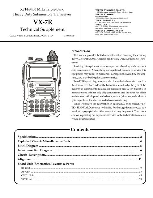
50/144/430 MHz Triple-BandHeavy Duty Submersible Transceiver<strong>VX</strong>-<strong>7R</strong><strong>Technical</strong> <strong>Supplement</strong>©2003 VERTEX STANDARD CO., LTD. EH009M90BVERTEX STANDARD CO., LTD.4-8-8 Nakameguro, Meguro-Ku, Tokyo 153-8644, JapanVERTEX STANDARDUS Headquarters10900 Walker Street, Cypress, CA 90630, U.S.A.YAESU EUROPE B.V.P.O. Box 75525, 1118 ZN Schiphol, <strong>The</strong> NetherlandsYAESU UK LTD.Unit 12, Sun Valley Business Park, Winnall CloseWinchester, Hampshire, SO23 0LB, U.K.VERTEX STANDARD HK LTD.Unit 5, 20/F., Seaview Centre, 139-141 Hoi Bun Road,Kwun Tong, Kowloon, Hong KongDWIntroductionThis manual provides the technical information necessary for servicingthe <strong>VX</strong>-<strong>7R</strong> 50/144/430 MHzTriple-Band Heavy Duty Submersible Transceiver.Servicing this equipment requires expertise in handing surface-mountchip components. Attempts by non-qualified persons to service thisequipment may result in permanent damage not covered by the warranty,and may be illegal in some countries.Two PCB layout diagrams provided for each double-sided board inthis transceiver. Each side of the board is referred to by the type of themajority of components installed on that side ("Side A" or "Side B"). Inmost cases one side has only chip components, and the other has eithera mixture of both chip and leaded components (trimmers, coils, electrolyticcapacitors, ICs, etc.), or leaded components only.While we believe the information in this manual to be correct, VER-TEX STANDARD assumes no liability for damage that may occur as aresult of typographical or other errors that may be present. Your cooperationin pointing out any inconsistencies in the technical informationwould be appreciated.ContentsSpecification ............................................................................................................................................ 2Exploded View & Miscellaneous Parts .............................................................................................4Block Diagram ........................................................................................................................................ 5Interconnection Diagram ...................................................................................................................... 6Circuit Description................................................................................................................................ 7Alignment .............................................................................................................................................. 11Board Unit (Schematics, Layouts & Parts)RF Unit ............................................................................................................................................................................. 19AF Unit ............................................................................................................................................................................ 33CNTL Unit ....................................................................................................................................................................... 45VCO Unit ......................................................................................................................................................................... 591
SpecificationsGeneralFrequency Ranges:Channel Steps:Frequency Stability:Emission Type:Antenna Impedance:Supply Voltage:Current Consumption:Operating Temperature:Case Size:Weight:Rx (MAIN):0.5 - 1.8 MHz (BC Band)1.8 - 30 MHz (SW Band)30-59 MHz (50 MHz HAM: USA version)30-76 MHz (50 MHz HAM: EXP version)59-108 MHz (FM: USA version)76-108 MHz (FM: EXP version)108-137 MHz (Air Band)137-174 MHz (144 MHz HAM)174-222 MHz (VHF-TV)222-225 MHz (220 MHz HAM: USA version)225-420 MHz (ACT1: Action Band 1: USA version)222-420 MHz (ACT1: Action Band 1: EXP version)420-470 MHz (430 MHz HAM)470-729 MHz (UHF-TV: USA version)470-800 MHz (UHF-TV: EXP version)800-999 MHz (ACT2: Action Band 2, cellular Blocked)Rx (SUB):50 - 54 MHz137 - 174 MHz420 - 470 MHzTx: 50 - 54 MHz (MAIN & SUB)144 - 146 MHz or 144 - 148 MHz (MAIN & SUB)222-225 MHz (MAIN, USA version)430 - 440 MHz or 430 - 450 MHz (MAIN & SUB)5/9/10/12.5/15/20/25/50/100 kHz±5 ppm (+14°F to +122°F, –10°C to +50°C)F2, F3, A350-ohmNominal: 7.4 V DC, Negative GroundOperating: 10 - 16 V DC, Negative Ground (EXT DC jack)150 mA (Mono Band Receive)200 mA (Dual Band Receive)55 mA (Mono Band Receive, Standby, Saver Off)100 mA (Dual Band Receive, Standby, Saver Off)25 mA (Mono Band Receive, Standby, Saver On "Save Ratio 1:5")50 mA (Dual Band Receive, Standby, Saver On "Save Ratio 1:5")400 µA (Auto Power Off)1.6/1.3/1.0/0.7 A (50 MHz, Tx HI/L3/L2/L1)1.71.4/1.1/0.8 A (144 MHz, Tx HI/L3/L2/L1)0.6 A (220 MHz, Tx)1.8/1.5/1.2/0.9/ A (430 MHz, Tx HI/L3/L2/L1)–4°F to +140°F (–20°C to +60°C)60 (W) x 90 (H) x 28 (D) mm (w/o knob & antenna)250 g2
TransmitterRF Power Output:Modulation Type:Maximum Deviation:Spurious Emission:Microphone Impedance:ReceiverCircuit Type:Intermediate Frequencies:Sensitivity:Selectivity:AF Output:5/2.5/1.0/0.5 W (50/144/430 MHz, FM)0.3 W (220 MHz, FM)1.0 W (50 MHz, FM)FM: Variable ReactanceAM: Early Stage (Low Level)±5/±2.5 kHzAt least 60 dB below (@ Tx 1W)2 k-ohmN-FM, AM: Double-Conversion SuperheterodyneW-FM: Triple-Conversion Superheterodyne1st: 47.25 MHz (N-FM, AM)45.8 MHz (W-FM)2nd: 450 kHz (N-FM, AM)10.7 MHz (W-FM)3rd: 1 MHz (W-FM)3.0 µV for 10 dB SINAD (0.5 - 30 MHz, AM)0.5 µV for 12 dB SINAD (30 - 50 MHz, N-FM)0.16 µV for 12 dB SINAD (50 - 54 MHz, N-FM)15 kHz/35 kHz (-6 dB/-60 dB: N-FM, AM)200 kHz/300 kHz (-6 dB/-20 dB: W-FM)200 mW @ 8 ohm for 10 % THD (@ 7.4V DC)400 mW @ 8 ohm for 10 % THD (@ 13.8V DC)SpecificationsSpecifications are subject to change without notice, and are guaranteed within amateur bands only.3
Exploded View & Miscellaneous PartsRA0417100PANEL FRAMERA0399500WINDOWRA0399400DOUBLE FACE TAPERA0401600O RINGRA0399800LIGHT GUIDE (LED)Q7000426LCD MODULERA0399100LIGHT GUIDE (LED)RA0399900REFLECTOR SHEETRA0405600MIC HOLDER RUBBERCNTL-UnitAF-UnitP1091150CONNECTOR (MIC/SP)➂➈➆➆➈➂➂ ➂RA0400000RUBBER PACKING➉➆➈➉➆➈➀ U9900137 BINDING HEAD SCREW M2X21.7 (W/ O RING) 2➁ U9900138 BINDING HEAD SCREW M2X5 (W/ O RING) 4➂ U07225120 PAN HEAD SCREW M2X2.5SUS#1 4➃ U9900136 SPECIAL SCREW M2X2.35 1➄ RA0304300 WASHER 1➅ U00103002 PAN HEAD SCREW M2X3NI 1➆ U00104002 PAN HEAD SCREW M2X4NI 6➇ U9900140 TAPTITE SCREW M2X6SUS#3 2➈ U44104002 TAPTITE SCREW M2X4NI 4➉ U9900141 TAPTITE SCREW M1.7X5NI#3 2U07125102 TAPTITE SCREW M1.7X2.5SUS#1 2<strong>VX</strong>STD P/NQ3000183Q3000185Q8101014Q8101015Q9000786Q9500087Q9500088Q9500089Q9500090RA029630AS6000335CP7346002 (USA, SILVER)CP7346003 (EXPORT, SILVER)CP7346004 (GERMANY, SILVER)CP7346006 (USA, BLACK)CP7346007 (EXPORT, BLACK)CP7346008 (GERMANY, BLACK)PANEL ASS’Ywith RUBBER KNOB, MIC SHEET,SP SHEET, SP, PROTECTOR L,PROTECTOR RRA014250ADOUBLE FACE TAPE (LCD)SUPPLIED ACCESSORIESDISCRIPTIONYHA-64 (depending on transceiver version)YHA-65YHA-63 50MHZ ADAPTER LYHA-63 440MHZ ADAPTER SLI-ION BATTERY FNB-80LINC-72ANC-72B (depending on transceiver version)NC-72CNC-72UBELT CLIPHAND STRAPFR008330CFPC CABLE<strong>The</strong>re is a direction inWASHER.EXP CAPSCREWWASHERRA0426800O RINGRA0400900O RINGRF-UnitRA0400500EXT CAPRA0292200SPECIAL NUTRA0426900O RINGRA0087900SPECIAL NUTRA0401200ENCODER KNOBRA0401900VOLUME KNOBRA0400600CAP(SP/MIC)➃➄➁➇ ➇➀➆ ➆➅➀➁➁➁RA0400200STUD (X4 pcs)P0091335CONNECTOR (EXT DC)RA01403AALATCH NAILCP7342003 (SILVER)CP7342005 (BLACK)REAR CASE ASS’Ywith SMA CONNECTOR ASS’Y,TERMINAL BOARD ASS’Y,RUBBER HOLDER (PTT),RUBBER KNOB (PTT)RA0399700HOLDER (PTT)RA0400100RUBBER KNOB (PTT)RA0140100MASK SHEETRA0141600RUBBER PACKINGFNB-80LI4
Block Diagram5
Interconnection Diagram6
Circuit Descriptionpassed through a band-pass filter to first mixer Q1013(2SC4915-0). Meanwhile, HF output from the VCO-UNITis amplified by Q1018 and applied through diode T/Rswitch D1046 to mixer Q1013 as the first local signal.<strong>The</strong> 47.25-MHz intermediate frequency product of themixer is delivered to the AF-UNIT.<strong>The</strong> TUNE voltage from the CPU on the CNTL-UNIT isamplified by DC amplifier Q3017 and applied to varactorsD1013 (HVR100) in the variable frequency band-passfilters. By changing the electrostatic capacitance of thevaractors, optimum filter characteristics are provided foreach specific operating frequency.(6) 540 - 999 MHz ReceptionReceived signals between 540 and 999 MHz passthrough the high-pass filter circuit, T/R switch D1004(1SV271) prior to application to RF amplifier Q1002(2SC5277). <strong>The</strong> amplified RF signal is passed through aband-pass filter to first mixer Q1010 (2SC5277). Meanwhile,UHF output from the VCO-UNIT is amplified byQ1016 and applied through diode T/R switch D1045 tomixer Q1010 as the first local signal.<strong>The</strong> 47.25-MHz intermediate frequency product of themixer is delivered to the AF-UNIT.<strong>The</strong> TUNE voltage from the CPU on the CNTL-UNIT isamplified by DC amplifier Q3017 and applied to varactorsD1015 and D1017 (HVC355B) in the variable frequencyband-pass filters. By changing the electrostatic capacitanceof the varactors, optimum filter characteristics areprovided for each specific operating frequency.(7) 47.25-MHz First Intermediate Frequency<strong>The</strong> 47.25-MHz first intermediate frequency from thefirst mixers is delivered from the RF-UNIT to the AF-UNITthrough jacks J1008 and J2001. On the AF-UNIT, the IFfor AM and FM-narrow signals is passed through NAR/WIDE switch D2001 (DAP222) and the 47.25-MHz monolithiccrystal filter (MCF) XF2001 to narrow IF amplifierQ2002 (2SC4915-0) for input to pin 16 of the Narrow IFIC Q2016 (TA31136FN), after amplitude limiting by D2003(DA221).Meanwhile, a portion of the output of 11.7-MHz crystalX1001 on the RF-UNIT is multiplied fourfold by Q2004(2SC4915-0) and Q2012 (2SC4154E) to provide the 46.8-MHz second local signal, applied to the Narrow IF IC.Within the IC, this signal is mixed with the 47.25-MHzfirst intermediate frequency signal to produce the 450 kHzsecond intermediate frequency.This second IF is filtered by ceramic filter CF2002(ALFYM450F=k) and amplified by the limiting amplifierwithin the Narrow IF IC before quadrature detection byceramic discriminator CD2001 (CDBM450C7).Demodulated audio is passed from pin 9 of the NarrowIF IC through the "Mute" analog switch Q2029 (2SJ364)and squelch gate Q2036 (2SJ364) before de-emphasis atQ2028 (DTC144EE).<strong>The</strong> resulting audio is amplified by AF amplifier Q2040(TDA7233D) and fed through the MIC/EAR jack J2002 tointernal speaker SP1001 or an external earphone.(8) Squelch ControlSignal components in the neighborhood of 15 kHz containedin the discriminator output pass through an activeband-pass filter composed of R2059, R2060, R2062, C2076,C2078 and the operational amplifier between pins 7 and8 within Narrow IF IC Q2016. <strong>The</strong>y are then rectified byD2012 and D2013 (MC2850) to obtain a DC voltage correspondingto the level of noise. This voltage is fed to pin49 of CPU Q3035 (HD6472237TF10), which compares theinput voltage with a previously set threshold. When theinput voltage drops below the threshold, normally due tothe presence of a carrier, the CPU turns on squelch gateQ2036 and allows any demodulated audio to pass. At thesame time, Q3001 and/or Q3003 and/or Q3004 goes on,causing the BUSY/TX lamp D3033 (FRGB1312CE-10-TF)to light.Transmitter Signal Flow(1) 145-MHz-Band Transmit/Receive SwitchingClosing PTT switch S2002 on the AF-UNIT pulls the baseof Q3008 (DTA144EE) low, causing the collector to gohigh. This signal is fed to pin 33 (PTT) of CPU Q3035,allowing the CPU to recognize that the PTT switch hasbeen pushed. When the CPU detects closure of the PTTswitch, pin 10 (TX) goes high. This control signal is deliveredto the RF-UNIT, where it switches Q1044 (UMW1)and Q1043 (CPH6102) to produce the TX control signalthat activates Q1046 (2SA1774). At the same time, PLLdivision data is fed to PLL IC Q1019 (MB15A01PFV1)from the CPU, to disable the receiver power saver. Also,it switches Q1048 (KRC654U) to disable the receiver circuits.This causes the "red" mode of BUSY/TX lamp D3033to light.8
Circuit Description(2) ModulationVoice signal input from either built-in microphoneMC3001 (EM-140) on the CNTL-UNIT or external jackJ2002 on the AF-UNIT is pre-emphasized by C3012 andR3031, and processed by microphone amplifier Q3018(NJM3403AV), IDC (instantaneous deviation control) circuitQ1014 to prevent overmodulation, and fed throughactive low-pass filter Q1014.During CTCSS operation, the voice signal is mixed withthe TONE ENC subaudible tone signal from pin 43 of theCPU and delivered to the RF-UNIT through jacks J3003and J1008. During DTMF operation, the DTMF tones frompin 44 of the CPU are fed to the IDC stage.(3) 145-MHz-Band TransmissionModulating audio from the CNTL-UNIT passes throughdeviation setting D/A converter Q3012 to the VHF modulatorportion of the VCO-UNIT mounted on the RF-UNIT.This signal is applied to varactor D4005 (HSC277) in thetank circuit of VHF VCO Q4004 (EC3H07B), which oscillatesat the desired VHF transmitting frequency. <strong>The</strong>modulated VCO signal is buffered by amplifier Q4006(EC3H07B) and Q1017 and delivered through VHF T/Rdiode switch D1041 to the RF-UNIT. <strong>The</strong> modulated lowlevelVHF transmit signal from the VCO is passed throughdiode switch D1043 (DAN222) to amplifier Q1014(2SC5226-5). <strong>The</strong> modulated VHF transmit signal fromthe VCO is amplified by Q1023 (2SK3475) and RF poweramplifier Q1027 (2SK3476) up to 0.05, 1.0, 2.5 or 5 Watts(depending on the power source). <strong>The</strong> RF output passesthrough TX diode switch D1053. RF output is passed bythe T/R switch and low-pass filter to suppress harmonicsand spurious products before output gets to the antennaat the antenna terminal.(4) 435-MHz-Band TransmissionModulating audio from the CNTL-UNIT passes throughdeviation setting D/A converter Q3012 to the UHF modulatorportion of the VCO-UNIT mounted on the RF-UNIT. This signal is applied to varactor D4002 (HSC277)in the tank circuit of UHF VCO Q4002 (EC3H07B), whichoscillates at the desired UHF transmitting frequency. <strong>The</strong>modulated VCO signal is buffered by amplifier Q4006 andQ1016 and delivered through UHF T/R diode switchD1045 to the RF-UNIT. <strong>The</strong> modulated low-level UHFtransmit signal from the VCO is passed through diodeswitch D1045 (HN2D01FU) to amplifier Q1014. <strong>The</strong> modulatedUHF transmit signal from the VCO is amplifiedby Q1023 and RF power amplifier Q1027 up to 0.05, 1.0,2.5 or 5 Watts (depending on the power source). <strong>The</strong> RFoutput passes through TX diode switch D1048. RF outputis passed through the T/R switch and low-pass filterto suppress harmonics and spurious products before outputgets to the antenna at the antenna terminal.(5) 50-MHz-Band TransmissionModulating audio from the CNTL-UNIT passes throughdeviation setting D/A converter Q3012 to the 50 MHzmodulator portion of the VCO-UNIT mounted on the RF-UNIT. This signal is applied to varactor D4009 (HSC277)in the tank circuit of 50 MHz VCO Q4005 (EC3H07B),which oscillates at the desired 50 MHz transmitting frequency.<strong>The</strong> modulated VCO signal is buffered by amplifierQ4006 and Q1018 and delivered through 50 MHz T/Rdiode switch D1046 to the RF-UNIT. <strong>The</strong> modulated lowlevel50 MHz transmit signal from the VCO is passedthrough diode switch D1046 (HN2D01FU) to amplifierQ1014. <strong>The</strong> modulated 50 MHz transmit signal from theVCO is amplified by Q1023 and RF power amplifier Q1027up to 0.05, 1.0, 2.5 or 5 Watts (depending on the powersource). <strong>The</strong> RF output passes through TX diode switchD1058. RF output is passed through the T/R switch andlow-pass filter to suppress harmonics and spurious productsbefore output gets to the antenna at the antenna terminal.9
Circuit DescriptionPLL Frequency SynthesizerPLL IC Q1019 on the RF-UNIT consists of a data shiftregister, reference frequency divider, phase comparator,charge pump, "intermittent operation" circuit, and bandselector switch. Serial PLL data from the CPU is convertedinto parallel data by the shift register in the PLL ICand is latched into the comparative frequency divider andreference frequency divider to set a frequency dividingratio for each. An 11.7-MHz reference signal producedby X1001 is fed to "REF" pin 1 of the PLL IC. <strong>The</strong> internalreference frequency divider divides the 11.7-MHz referenceby 2,050 (or 1,640) to obtain a reference frequency of5 kHz (or 6.25 kHz), which is applied to the phase comparator.Meanwhile, a sample of the output of VHF VCOQ4004 or UHF VCO Q4002 or 50 MHz VCO Q4005 on theVCO-UNIT, buffered by Q4006, is fed to the PLL IC, whereit is divided by the internal comparative frequency dividerto produce a comparative frequency which also is appliedto the phase comparator. <strong>The</strong> phase comparator comparesthe phase between the reference frequency and comparativefrequency to output a pulse corresponding to thephase difference between them. This pulse is fed to thecharge pump, and the output from the charge pump passesthrough a loop filter composed of L1044, R1089, C1175,and either R1090, C1192, R1103 and C1195 for VHF, orR1086, C1189, R1102 and C1194 for UHF, or R1091, C1193,R1104 and C1196 for 50 MHz, which convert the pulseinto a corresponding smoothed varactor control voltage(VCV). <strong>The</strong> VCV is applied to varactors D4004 and D4013(1SV325) in the VHF VCO tank circuit, or to varactorD4001 (HVC355B) in the UHF VCO tank circuit, or tovaractors D4007 and D4008 (1SV325) in the 50 MHz VCO,to eliminate any phase difference between the referencefrequency and comparative frequency, thus locking theVCO oscillation frequency to the reference crystal. <strong>The</strong>VCO frequency is determined by the frequency-dividingratio sent from the CPU to the PLL IC. During receiverpower save operation, the PLL circuit operates intermittentlyto reduce current consumption, for which the "intermittentoperation" control circuit reduces the lock-uptime.10
DWAlignmentIntroduction and Precautions<strong>The</strong> <strong>VX</strong>-<strong>7R</strong> has been carefully aligned at the factory forthe specified performance across the specified amateurbands. Realignment should therefore not be necessaryexcept in the event of a component failure. All componentreplacement and service should be performed onlyby an authorized VERTEX STANDARD representative,or the warranty policy may be voided.<strong>The</strong> following procedures cover the sometimes criticaland tedious adjustments that are not normally requiredonce the transceiver has left the factory. However, if damageoccurs and some parts are replaced, realignment maybe required. If a sudden problem occurs during normaloperation, it is likely due to component failure; realignmentshould not be done until after the faulty componenthas been replaced.We recommend that servicing be performed only byauthorized VERTEX STANDARD service technicians,who are experienced with the circuitry and fully equippedfor repair and alignment. <strong>The</strong>refore, if a fault is suspected,contact the dealer from whom the transceiver waspurchased for instructions regarding repair. AuthorizedVERTEX STANDARD service technicians realign all circuitsand make complete performance checks to ensurecompliance with factory specifications after replacing anyfaulty components.Those who do undertake any of the following alignmentsare cautioned to proceed at their own risk. Problemscaused by unauthorized attempts at realignment arenot covered by the warranty policy. Also, VERTEX STAN-DARD must reserve the right to change circuits and alignmentprocedures in the interest of improved performance,without notifying owners.Under no circumstances should any alignment be attemptedunless the normal function and operation of thetransceiver are clearly understood, the cause of the malfunctionhas been clearly pinpointed and any faulty componentsreplaced, and the need for realignment determinedto be absolutely necessary.Required Test Equipment❍ RF Signal Generator with calibrated output level at 500 MHz❍ Deviation Meter (linear detector)❍ In-line Wattmeter with 5% accuracy at 500 MHz❍ 50-ohm, 10-W RF Dummy Load❍ 8-ohm AF Dummy Load❍ Regulated DC Power Supply adjustable from 3 to 15 V DC, 3A❍ Frequency Counter: 0.2-ppm accuracy at 500 MHz❍ AF Signal Generator❍ AC Voltmeter❍ DC Voltmeter: high impedance❍ UHF Sampling Coupler❍ SINAD MeterAlignment Preparation & PrecautionsA 10-W RF dummy load and in-line wattmeter must beconnected to the main antenna jack in all procedures thatcall for transmission, alignment is not possible with anantenna. After completing one step, read the next step tosee if the same test equipment is required. If not, removethe test equipment (except dummy load and wattmeter,if connected) before proceeding.Correct alignment requires that the ambient temperaturebe the same as that of the transceiver and test equipment,and that this temperature be held constant between68~86°F (20~30°C). When the transceiver is brought intothe shop from hot or cold air, it should be allowed sometime to come to room temperature before alignment.Whenever possible, alignments should be made with oscillatorshields and circuit boards firmly affixed in place.Also, the test equipment must be thoroughly warmed upbefore beginning.Note: Signal levels in dB referred to in the alignment procedureare based on 0 dBµ=0.5 µV (closed circuit).50-ohmRF LoadRF SignalGeneratorIn-LineWattmeterDeviationMeterSamplingCoupler8-ohmAF LoadSINADMeterFrequencyCounterAlignment Setup11
AlignmentTest SetupSet up the test equipment as shown below for transceiveralignment, and apply 8.7 V DC power to the transceiver.Refer to the drawings for Alignment Points.Internal System Alignment RoutineThis uses a programmed routine in the transceiverwhich simplifies many previously complex discrete componentsettings and adjustments with digitally-controlledsettings via front panel buttons and LCD indications.To begin, set the transceiver to the center of the 50 MHz,144 MHz, 222 MHz and 430 MHz bands. Next, select the430 MHz band, then turn the transceiver off.Now, press and hold in the MON/F, and 0 buttons (atthe same time) while powering the radio on again. <strong>The</strong>display will show the first setting. <strong>The</strong>reafter, the frequenciesused during alignment will automatically be set withoutaction by the technician.In the alignment process, each adjustment is selectedby rotating the DIAL. Alignment is performed by:12❍ Pressing the V/M button;❍ Injecting a signal of the required frequency and level;then❍ Pressing the V/M button after a level setting or adjustmentis made. This second pressing of the MON/F button stores the entry.To exit the alignment routine, press the HM/RV button.After performing the system alignment in its entirety, individualsettings can be returned to and adjusted shouldthe need arise.As each transceiver is individually optimized at the factory,the precise settings for the transceiver on your benchmay be slightly different.Main Band AlignmentPLL Reference Frequency (PLL REF)Press the V/M button, then transmit and adjust the counterfrequency to 440.000 (±300 Hz) by rotating the DIAL, thenpress the V/M button. Rotate the DIAL to select the nextsetting.430 MHz band AlignmentSquelch Hysteresis Adjustment (HIS SQL)❍ Rotate the DIAL for minimum squelch hysteresis. Pressthe V/M button, then rotate the DIAL to select the nextsetting.Squelch Preset Threshold (THLD SQL) [86]❍ Inject a –15.0 dBµ RF signal (1 kHz tone @ ±3.5 kHzdeviation), then press the V/M button, then press theMON/F button twice. Press the V/M button, then rotatethe DIAL to select the next setting.Squelch Preset Tight (TIGH SQL)❍ Adjust the generator level to –5.0 dBµ, then press the V/M button, then press the MON/F button twice. Press theV/M button, then rotate the DIAL to select the next setting.S-Meter S-1 Adjustment (S1 LEVEL)❍ Adjust the generator level to –7.0 dBµ (1 kHz tone @±3.5 kHz deviation), then press the V/M button, thenpress the MON/F button twice. Press the V/M button, thenrotate the DIAL to select the next setting.S-Meter Full-Scale Adjustment (S9 LEVEL)❍ Adjust the generator level to +19 dBµ (1 kHz tone @±3.5 kHz deviation), then press the V/M button, thenpress the MON/F button twice. Press the V/M button, thenrotate the DIAL to select the next setting.Wide-FM S-Meter S-1 Adjustment (S1 LEVEL)❍ Adjust the generator level to 0 dBµ (1 kHz tone @ ±20kHz deviation), then press the V/M button, then pressthe MON/F button twice. Press the V/M button, then rotatethe DIAL to select the next setting.Wide-FM S-Meter Full-Scale Adjustment (S9 LEVEL)❍ Adjust the generator level to +20 dBµ (1 kHz tone @ ±20kHz deviation), then press the V/M button, then pressthe MON/F button twice. Press the V/M button, then rotatethe DIAL to select the next setting.<strong>The</strong> alignment frequency will now be automatically setto 430.000 MHz.High TX Power Adjustment (HI POWER)❍ Transmit, and adjust the output power level for 5.0 W(±0.3 W) by rotating the DIAL, then press the V/M button.Rotate the DIAL to select the next setting.L3 Tx Power Adjustment (L3 POWER)❍ Transmit, and adjust the output power level for 2.5 W(±0.2 W) by rotating the DIAL, then press the V/M button.Rotate the DIAL to select the next setting.L2 Tx Power Adjustment (L2 POWER)❍ Transmit, and adjust the output power level for 1.0 W(±0.1 W) by rotating the DIAL, then press the V/M button.Rotate the DIAL to select the next setting.
AlignmentL1 Tx Power Adjustment (L1 POWER)❍ Transmit, and adjust the output power level for 50 mW(+50/-30 mW) by rotating the DIAL, then press the V/Mbutton. Rotate the DIAL to select the next setting.TX Deviation Adjustment (MAX DEV)❍ Inject a 1 kHz audio tone at a level of 50 mV (rms) to theMIC jack. Press the V/M button, then transmit and adjustthe deviation for 4.5 kHz (±0.2 kHz) (USA Version:4.2 kHz (±0.2 kHz)) by rotating the DIAL, then press theV/M button. Rotate the DIAL to select the next setting.CTCSS Tx Deviation Adjustment (TN 67.0)❍ Press the V/M button, then transmit and adjust the deviationfor 0.5 kHz (+0.05/-0.1 kHz) by rotating the DIAL,then press the V/M button. Rotate the DIAL to select thenext setting.CTCSS Tx Deviation Adjustment (TN 183.5)❍ Press the V/M button, then transmit and adjust the deviationfor 0.5 kHz (±0.1 kHz) by rotating the DIAL, thenpress the V/M button. Rotate the DIAL to select the nextsetting.CTCSS Tx Deviation Adjustment (TN 254.1)❍ Press the V/M button, then transmit and adjust the deviationfor 0.5 kHz (±0.1 kHz) by rotating the DIAL, thenpress the V/M button. Rotate the DIAL to select the nextsetting.DCS Tx Deviation Adjustment (DCS DEV)❍ Press the V/M button, then transmit and adjust the deviationfor 0.6 kHz (±0.1 kHz) by rotating the DIAL, thenpress the V/M button. Rotate the DIAL to select the nextsetting.Press the MON/F to activate the TX Power and Deviationalignment routine.<strong>The</strong> alignment frequency will automatically be set to440.000 MHz (USA Version: 450.000 MHz).High TX Power Adjustment (HI POWER)❍ Transmit, and adjust the output power level for 5.0 W(±0.3 W) by rotating the DIAL, then press the V/M button.Rotate the DIAL to select the next setting.High TX Power Adjustment (L3 POWER)❍ Transmit, and adjust the output power level for 2.5 W(±0.2 W) by rotating the DIAL, then press the V/M button.Rotate the DIAL to select the next setting.High TX Power Adjustment (L2 POWER)❍ Transmit, and adjust the output power level for 1.0 W(±0.1 W) by rotating the DIAL, then press the V/M button.Rotate the DIAL to select the next setting.High TX Power Adjustment (L1 POWER)❍ Transmit, and adjust the output power level for 50 mW(+50/-30 mW) by rotating the DIAL, then press the V/Mbutton. Rotate the DIAL to select the next setting.TX Deviation Adjustment (MAX DEV)❍ Inject a 1 kHz audio tone at a level of 50mV (rms) to theMIC jack. Press the V/M button, then transmit and adjustthe deviation for 4.5 kHz (±0.2 kHz) (USA Version: 4.2kHz (±0.1 kHz)) by rotating the DIAL, then press the V/Mbutton. Rotate the DIAL to select the next setting.CTCSS Tx Deviation Adjustment (TN 67.0)❍ Press the V/M button, then transmit and adjust the deviationfor 0.5 kHz (+0.05/-0.1 kHz) by rotating the DIAL,then press the V/M button. Rotate the DIAL to select thenext setting.CTCSS Tx Deviation Adjustment (TN 183.5)❍ Press the V/M button, then transmit and adjust the deviationfor 0.5 kHz (±0.1 kHz) by rotating the DIAL, thenpress the V/M button. Rotate the DIAL to select the nextsetting.CTCSS Tx Deviation Adjustment (TN 254.1)❍ Press the V/M button, then transmit and adjust the deviationfor 0.5 kHz (±0.1 kHz) by rotating the DIAL, thenpress the V/M button. Rotate the DIAL to select the nextsetting.DCS Tx Deviation Adjustment (DCS DEV)❍ Press the V/M button, then transmit and adjust the deviationfor 0.6 kHz (±0.1 kHz) (USA Version: 0.9 kHz(±0.1 kHz)) by rotating the DIAL, then press the V/Mbutton. Rotate the DIAL to select the next setting.Press the BAND button to activate the 50 MHz bandinternal alignment routine.<strong>The</strong> alignment frequency will automatically be set to52.100 MHz.50 MHz Band AlignmentSquelch Hysteresis Adjustment (HIS SQL)❍ Rotate the DIAL for minimum squelch hysteresis. Pressthe V/M button, then rotate the DIAL to select the nextsetting.13
AlignmentSquelch Preset Threshold (THLD SQL)❍ Inject a –15.0 dBµ RF signal (1 kHz tone @ ±3.5 kHzdeviation), then press the V/M button, then press theMON/F button twice. Press the V/M button, then rotatethe DIAL to select the next setting.Squelch Preset Tight (TIGH SQL)❍ Adjust the generator level to –4.0 dBµ, then press the V/Mbutton, then press the MON/F button twice. Press the V/Mbutton, then rotate the DIAL to select the next setting.S-Meter S-1 Adjustment (S1 LEVEL)❍ Adjust the generator level to –7.0 dBµ (1 kHz tone @±3.5 kHz deviation), then press the V/M button, thenpress the MON/F button twice. Press the V/M button, thenrotate the DIAL to select the next setting.S-Meter Full-Scale Adjustment (S9 LEVEL)❍ Adjust the generator level to +19 dBµ (1 kHz tone @±3.5 kHz deviation), then press the V/M button, thenpress the MON/F button twice. Press the V/M button, thenrotate the DIAL to select the next setting.Wide-FM S-Meter S-1 Adjustment (S1 LEVEL)❍ Adjust the generator level to 0 dBµ (1 kHz tone @ ±20kHz deviation), then press the V/M button, then pressthe MON/F button twice. Press the V/M button, then rotatethe DIAL to select the next setting.Wide-FM S-Meter Full-Scale Adjustment (S9 LEVEL)❍ Adjust the generator level to +20 dBµ (1 kHz tone @ ±20kHz deviation), then press the V/M button, then pressthe MON/F button twice. Press the V/M button, then rotatethe DIAL to select the next setting.<strong>The</strong> alignment frequency will now be automatically setto 50.000 MHz.High TX Power Adjustment (HI POWER)❍ Transmit, and adjust the output power level for 5.0 W(±0.3 W) by rotating the DIAL, then press the V/M button.Rotate the DIAL to select the next setting.L3 Tx Power Adjustment (L3 POWER)❍ Transmit, and adjust the output power level for 2.5 W(±0.2 W) by rotating the DIAL, then press the V/M button.Rotate the DIAL to select the next setting.L2 Tx Power Adjustment (L2 POWER)❍ Transmit, and adjust the output power level for 1.0 W(±0.1 W) by rotating the DIAL, then press the V/M button.Rotate the DIAL to select the next setting.14L1 Tx Power Adjustment (L1 POWER)❍ Transmit, and adjust the output power level for 50 mW(+50/-30 mW) by rotating the DIAL, then press the V/Mbutton. Rotate the DIAL to select the next setting.TX Deviation Adjustment (MAX DEV)❍ Inject a 1 kHz audio tone at a level of 50mV (rms) to theMIC jack. Press the V/M button, then transmit and adjustthe deviation for4.5 kHz (±0.2 kHz) (USA Version: (4.2±0.2 kHz)) by rotating the DIAL, then press the V/M button.Rotate the DIAL to select the next setting.AM Modulation (AM MOD)❍ Inject a 1 kHz audio tone at a level of 100 mV (rms) tothe MIC jack. Press the V/M button, then transmit andadjust the modulation for 60% (±10%) by rotating theDIAL, then press and hold in the MON/F button for onesecond.CTCSS Tx Deviation Adjustment (TN 67.0)❍ Press the V/M button, then transmit and adjust the deviationfor 0.6 kHz (+0.05/-0.1 kHz) by rotating the DIAL,then press the V/M button. Rotate the DIAL to select thenext setting.CTCSS Tx Deviation Adjustment (TN 167.9)❍ Press the V/M button, then transmit and adjust the deviationfor 0.6 kHz (+0.05/-0.1 kHz) by rotating the DIAL,then press the V/M button. Rotate the DIAL to select thenext setting.CTCSS Tx Deviation Adjustment (TN 254.1)❍ Press the V/M button, then transmit and adjust the deviationfor 0.6 kHz (+0.05/-0.1 kHz) by rotating the DIAL,then press the V/M button. Rotate the DIAL to select thenext setting.DCS Tx Deviation Adjustment (DCS DEV)❍ Press the V/M button, then transmit and adjust the deviationfor 0.6 kHz (±0.1 kHz) by rotating the DIAL, thenpress the V/M button. Rotate the DIAL to select the nextsetting.Press the MON/F button to activate the TX Power andDeviation alignment routine.<strong>The</strong> alignment frequency will automatically be set to54.000 MHz.High TX Power Adjustment (HI POWER)❍ Transmit, and adjust the output power level for 5.0 W(±0.3 W) by rotating the DIAL, then press the V/M button.Rotate the DIAL to select the next setting.
AlignmentHigh TX Power Adjustment (L3 POWER)❍ Transmit, and adjust the output power level for 2.5 W(±0.2 W) by rotating the DIAL, then press the V/M button.Rotate the DIAL to select the next setting.High TX Power Adjustment (L2 POWER)❍ Transmit, and adjust the output power level for 1.0 W(±0.1 W) by rotating the DIAL, then press the V/M button.Rotate the DIAL to select the next setting.High TX Power Adjustment (L1 POWER)❍ Transmit, and adjust the output power level for 50 mW(+50/-30 mW) by rotating the DIAL, then press the V/Mbutton. Rotate the DIAL to select the next setting.TX Deviation Adjustment (MAX DEV)❍ Inject a 1 kHz audio tone at a level of 50mV (rms) to theMIC jack. Press the V/M button, then transmit and adjustthe deviation for 4.5 kHz (±0.2 kHz) (USA Version:4.2 kHz (±0.2 kHz)) by rotating the DIAL, then press theV/M button. Rotate the DIAL to select the next setting.AM Modulation (AM MOD)❍ Inject a 1 kHz audio tone at a level of 100mV (rms) tothe MIC jack. Press the V/M button, then transmit andadjust the modulation for 60% (±10%) by rotating theDIAL.CTCSS Tx Deviation Adjustment (TN 67.0)❍ Press the V/M button, then transmit and adjust the deviationfor 0.6 kHz (+0.05/-0.1 kHz) by rotating the DIAL,then press the V/M button. Rotate the DIAL to select thenext setting.CTCSS Tx Deviation Adjustment (TN 167.9)❍ Press the V/M button, then transmit and adjust the deviationfor 0.6 kHz (+0.05/-0.1 kHz) by rotating the DIAL,then press the V/M button. Rotate the DIAL to select thenext setting.CTCSS Tx Deviation Adjustment (TN 254.1)❍ Press the V/M button, then transmit and adjust the deviationfor 0.6 kHz (+0.05/-0.1 kHz) by rotating the DIAL,then press the V/M button. Rotate the DIAL to select thenext setting.DCS Tx Deviation Adjustment (DCS DEV)❍ Press the V/M button, then transmit and adjust the deviationfor 0.6 kHz (±0.1 kHz) by rotating the DIAL, thenpress the V/M button. Rotate the DIAL to select the nextsetting.Press the BAND button to activate the 145 MHz bandinternal alignment routine.<strong>The</strong> alignment frequency will automatically be set to145.100 MHz (USA Version: 146.100 MHz).144 MHz Band AlignmentSquelch Hysteresis Adjustment (HIS SQL)❍ Rotate the DIAL for minimum squelch hysteresis. Pressthe V/M button, then rotate the DIAL to select the nextsetting.Squelch Preset Threshold (THLD SQL)❍ Inject a –15.0 dBµ RF signal (1 kHz tone @ ±3.5 kHzdeviation), then press the V/M button, then press theMON/F button twice. Press the V/M button, then rotatethe DIAL to select the next setting.Squelch Preset Tight (TIGH SQL)❍ Adjust the generator level to –4.0 dBµ, then press the V/M button, then press the MON/F button twice. Press theV/M button, then rotate the DIAL to select the next setting.S-Meter S-1 Adjustment (S1 LEVEL)❍ Adjust the generator level to –7.0 dBµ (1 kHz tone @±3.5 kHz deviation), then press the V/M button, thenpress the MON/F button twice. Press the V/M button, thenrotate the DIAL to select the next setting.S-Meter Full-Scale Adjustment (S9 LEVEL)❍ Adjust the generator level to +19 dBµ (1 kHz tone @±3.5 kHz deviation), then press the V/M button, thenpress the MON/F button twice. Press the V/M button, thenrotate the DIAL to select the next setting.Wide-FM S-Meter S-1 Adjustment (S1 LEVEL)❍ Adjust the generator level to 0 dBµ (1 kHz tone @ ±20kHz deviation), then press the V/M button, then pressthe MON/F button twice. Press the V/M button, then rotatethe DIAL to select the next setting.Wide-FM S-Meter Full-Scale Adjustment (S9 LEVEL)❍ Adjust the generator level to +20 dBµ (1 kHz tone @ ±20kHz deviation), then press the V/M button, then pressthe MON/F button twice. Press the V/M button, then rotatethe DIAL to select the next setting.<strong>The</strong> alignment frequency will now be automatically setto 144.000 MHz.15
AlignmentHigh TX Power Adjustment (HI POWER)❍ Transmit, and adjust the output power level for 5.0 W(±0.3 W) by rotating the DIAL, then press the V/M button.Rotate the DIAL to select the next setting.L3 Tx Power Adjustment (L3 POWER)❍ Transmit, and adjust the output power level for 2.5 W(±0.2 W) by rotating the DIAL, then press the V/M button.Rotate the DIAL to select the next setting.L2 Tx Power Adjustment (L2 POWER)❍ Transmit, and adjust the output power level for 1.0 W(±0.1 W) by rotating the DIAL, then press the V/M button.Rotate the DIAL to select the next setting.L1 Tx Power Adjustment (L1 POWER)❍ Transmit, and adjust the output power level for 50 mW(+50/-30 mW) by rotating the DIAL, then press the V/Mbutton. Rotate the DIAL to select the next setting.TX Deviation Adjustment (MAX DEV)❍ Inject a 1 kHz audio tone at a level of 50mV (rms) to theMIC jack. Press the V/M button, then transmit and adjustthe deviation for 4.5 kHz (±0.2 kHz) (USA Version:4.2 kHz (±0.2 kHz)) by rotating the DIAL, then press theV/M button. Rotate the DIAL to select the next setting.CTCSS Tx Deviation Adjustment (TN 67.0)❍ Press the V/M button, then transmit and adjust the deviationfor 0.6 kHz (+0.05/-0.1 kHz) by rotating the DIAL,then press the V/M button. Rotate the DIAL to select thenext setting.CTCSS Tx Deviation Adjustment (TN 151.4)❍ Press the V/M button, then transmit and adjust the deviationfor 0.6 kHz (+0.05/-0.1 kHz) by rotating the DIAL,then press the V/M button. Rotate the DIAL to select thenext setting.CTCSS Tx Deviation Adjustment (TN 254.1)❍ Press the V/M button, then transmit and adjust the deviationfor 0.6 kHz (+0.05/-0.1 kHz) by rotating the DIAL,then press the V/M button. Rotate the DIAL to select thenext setting.DCS Tx Deviation Adjustment (DCS DEV)❍ Press the V/M button, then transmit and adjust the deviationfor 0.6 kHz (±0.1 kHz) by rotating the DIAL, thenpress the V/M button. Rotate the DIAL to select the nextsetting.Press the MON/F to activate the TX Power and Deviationalignment routine.<strong>The</strong> alignment frequency will automatically be set to146.000 MHz (USA Version: 148.000 MHz).High TX Power Adjustment (HI POWER)❍ Transmit, and adjust the output power level for 5.0 W(±0.3 W) by rotating the DIAL, then press the V/M button.Rotate the DIAL to select the next setting.High TX Power Adjustment (L3 POWER)❍ Transmit, and adjust the output power level for 2.5 W(±0.2 W) by rotating the DIAL, then press the V/M button.Rotate the DIAL to select the next setting.High TX Power Adjustment (L2 POWER)❍ Transmit, and adjust the output power level for 1.0 W(±0.1 W) by rotating the DIAL, then press the V/M button.Rotate the DIAL to select the next setting.High TX Power Adjustment (L1 POWER)❍ Transmit, and adjust the output power level for 50 mW(+50/-30 mW) by rotating the DIAL, then press the V/Mbutton. Rotate the DIAL to select the next setting.TX Deviation Adjustment (MAX DEV)❍ Inject a 1 kHz audio tone at a level of 50mV (rms) to theMIC jack. Press the V/M button, then transmit and adjustthe deviation for 4.5 kHz (±0.2 kHz) (USA Version:4.2 kHz (±0.2 kHz)) by rotating the DIAL, then press theV/M button. Rotate the DIAL to select the next setting.CTCSS Tx Deviation Adjustment (TN 67.0)❍ Press the V/M button, then transmit and adjust the deviationfor 0.6 kHz (+0.05/-0.1 kHz) by rotating the DIAL,then press the V/M button. Rotate the DIAL to select thenext setting.CTCSS Tx Deviation Adjustment (TN 151.4)❍ Press the V/M button, then transmit and adjust the deviationfor for 0.6 kHz (+0.05/-0.1 kHz) by rotating theDIAL, then press the V/M button. Rotate the DIAL toselect the next setting.CTCSS Tx Deviation Adjustment (TN 254.1)❍ Press the V/M button, then transmit and adjust the deviationfor 0.6 kHz (+0.05/-0.1 kHz) by rotating the DIAL,then press the V/M button. Rotate the DIAL to select thenext setting.16
AlignmentDCS Tx Deviation Adjustment (DCS DEV)❍ Press the V/M button, then transmit and adjust the deviationfor 0.6 kHz (±0.1 kHz) by rotating the DIAL, thenpress the V/M button. Rotate the DIAL to select the nextsetting.NOTE: <strong>The</strong> next step depends on the geographical "version" ofthe transceiver being aligned:EXP Version: Alignment of the "SUB Band " follows (seepage 18.)USA Version: Press the BAND button to activate the222 MHz band internal alignment routine. In this case,the alignment frequency will automatically be set to222.000 MHz.222 MHz Band AlignmentL2 Tx Power Adjustment (L2 POWER)❍ Transmit, and adjust the output power level for 0.3 W(±0.1 W) by rotating the DIAL, then press the V/M button.Rotate the DIAL to select the next setting.L1 Tx Power Adjustment (L1 POWER)❍ Transmit, and adjust the output power level for 50 mW(+50/-30 mW) by rotating the DIAL, then press the V/Mbutton. Rotate the DIAL to select the next setting.TX Deviation Adjustment (MAX DEV)❍ Inject a 1 kHz audio tone at a level of 50mV (rms) to theMIC jack. Press the V/M button, then transmit and adjustthe deviation for 4.5 kHz (±0.2 kHz) (USA Version:4.2 kHz (±0.2 kHz)) by rotating the DIAL, then press theV/M button. Rotate the DIAL to select the next setting.CTCSS Tx Deviation Adjustment (TN 67.0)❍ Press the V/M button, then transmit and adjust the deviationfor 0.6 kHz (+0.05/-0.1 kHz) by rotating the DIAL,then press the V/M button. Rotate the DIAL to select thenext setting.CTCSS Tx Deviation Adjustment (TN 151.4)❍ Press the V/M button, then transmit and adjust the deviationfor 0.6 kHz (+0.05/-0.1 kHz) by rotating the DIAL,then press the V/M button. Rotate the DIAL to select thenext setting.CTCSS Tx Deviation Adjustment (TN 254.1)❍ Press the V/M button, then transmit and adjust the deviationfor 0.6 kHz (+0.05/-0.1 kHz) by rotating the DIAL,then press the V/M button. Rotate the DIAL to select thenext setting.DCS Tx Deviation Adjustment (DCS DEV)❍ Press the V/M button, then transmit and adjust the deviationfor 0.9 kHz (±0.1 kHz) by rotating DIAL, thenpress the V/M button. Rotate the DIAL to select the nextsetting.Press the to activate the TX Power and Deviationalignment routine.<strong>The</strong> alignment frequency will automatically be set to224.995 MHz.High Tx Power Adjustment (L2 POWER)❍ Transmit, and adjust the output power level for 0.3 W(+0.2/-0.1 W) by rotating the DIAL, then press the V/Mbutton. Rotate the DIAL to select the next setting.High Tx Power Adjustment (L1 POWER)❍ Transmit, and adjust the output power level for 50 mW(+50/-30 mW) by rotating the DIAL, then press the V/Mbutton. Rotate the DIAL to select the next setting.TX Deviation Adjustment (MAX DEV)❍ Inject a 1 kHz audio tone at a level of 50mV (rms) to theMIC jack. Press the V/M button, then transmit and adjustthe deviation for 4.5 kHz (±0.2 kHz) (USA Version:4.2 kHz (±0.2 kHz) by rotating DIAL, then press the V/M button. Rotate the DIAL to select the next setting.CTCSS Tx Deviation Adjustment (TN 67.0)❍ Press the V/M button, then transmit and adjust the deviationfor 0.6 kHz (+0.05/-0.1 kHz) by rotating the DIAL,then press the V/M button. Rotate the DIAL to select thenext setting.CTCSS Tx Deviation Adjustment (TN 151.4)❍ Press the V/M button, then transmit and adjust the deviationfor 0.6 kHz (+0.05/-0.1 kHz) by rotating theDIAL, then press the V/M button. Rotate the DIAL toselect the next setting.CTCSS Tx Deviation Adjustment (TN 254.1)❍ Press the V/M button, then transmit and adjust the deviationfor 0.6 kHz (+0.05/-0.1 kHz) by rotating the DIAL,then press the V/M button. Rotate the DIAL to select thenext setting.DCS Tx Deviation Adjustment (DCS DEV)❍ Press the V/M button, then transmit and adjust the deviationfor 0.9 kHz (±0.1 kHz) by rotating the DIAL, thenpress the V/M button. Rotate the DIAL to select the nextsetting.17
AlignmentPress the SUB button to activate the SUB band internalalignment routine.<strong>The</strong> alignment frequency will automatically be set to435.100 MHz (USA Version: 440.100 MHz) on the SUBband.SUB Band Alignment430 MHz Band AlignmentSquelch Hysteresis Adjustment (HIS SQL)❍ Rotate the DIAL for minimum squelch hysteresis. Pressthe V/M button, then rotate the DIAL to select the nextsetting.Squelch Preset Threshold (THLD SQL)❍ Inject a –13.0 dBµ RF signal (1 kHz tone @ ±3.5 kHzdeviation), then press the V/M button, then press theMON/F button twice. Press the V/M button, then rotatethe DIAL to select the next setting.Squelch Preset Tight (TIGH SQL)❍ Adjust the generator level to –6.0 dBµ, then press the V/Mbutton, then press the MON/F button twice. Press the V/Mbutton, then rotate the DIAL to select the next setting.S-Meter S-1 Adjustment (S1 LEVEL)❍ Adjust the generator level to –7.0 dBµ (1 kHz tone @±3.5 kHz deviation), then press the V/M button, thenpress the MON/F button twice. Press the V/M button, thenrotate the DIAL to select the next setting.S-Meter Full-Scale Adjustment (S9 LEVEL)❍ Adjust the generator level to +20 dBµ (1 kHz tone @±3.5 kHz deviation), then press the V/M button, thenpress the MON/F button twice. Press the V/M button.Press the BAND button to activate the 50 MHz SUB bandinternal alignment routine.<strong>The</strong> alignment frequency will automatically be set to52.100 MHz.50 MHz SUB Band AlignmentSquelch Hysteresis Adjustment (HIS SQL)❍ Rotate the DIAL for minimum squelch hysteresis. Pressthe V/M button, then rotate the DIAL to select the nextsetting.Squelch Preset Threshold (THLD SQL)❍ Inject a –13.0 dBµ RF signal (1 kHz tone @ ±3.5 kHzdeviation), then press the V/M button, then press theMON/F button twice. Press the V/M button, then rotatethe DIAL to select the next setting.Squelch Preset Tight (TIGH SQL)❍ Adjust the generator level to –4.0 dBµ, then press the V/M button, then press the MON/F button twice. Press theV/M button, then rotate the DIAL to select the next setting.S-Meter S-1 Adjustment (S1 LEVEL)❍ Adjust the generator level to –7.0 dBµ (1 kHz tone @±3.5 kHz deviation), then press the V/M button, thenpress the MON/F button twice. Press the V/M button, thenrotate the DIAL to select the next setting.S-Meter Full-Scale Adjustment (S9 LEVEL)❍ Adjust the generator level to +19 dBµ (1 kHz tone @±3.5 kHz deviation), then press the V/M button, thenpress the MON/F button twice. Press the V/M button.Press the BAND button to activate the 144 MHz SUB bandinternal alignment routine.<strong>The</strong> alignment frequency will automatically be set to145.100 MHz (USA Version: 146.100 MHz).144 MHz SUB Band AlignmentSquelch Hysteresis Adjustment (HIS SQL)❍ Rotate the DIAL for minimum squelch hysteresis. Press theV/M button, then rotate the DIAL to select the next setting.Squelch Preset Threshold (THLD SQL)❍ Inject a –15.0 dBµ RF signal (1 kHz tone @ ±3.5 kHzdeviation), then press the V/M button, then press theMON/F button twice. Press the V/M button, then rotatethe DIAL to select the next setting.Squelch Preset Tight (TIGH SQL)❍ Adjust the generator level to –6.0 dBµ, then press the V/Mbutton, then press the MON/F button twice. Press the V/Mbutton, then rotate the DIAL to select the next setting.S-Meter S-1 Adjustment (S1 LEVEL)❍ Adjust the generator level to –7.0 dBµ (1 kHz tone @±3.5 kHz deviation), then press the V/M button, thenpress the MON/F button twice. Press the V/M button, thenrotate the DIAL to select the next setting.S-Meter Full-Scale Adjustment (S9 LEVEL)❍ Adjust the generator level to +19 dBµ (1 kHz tone @±3.5 kHz deviation), then press the V/M button, thenpresses the MON/F button twice. Press the V/M button.This completes the internal alignment routine for all bands.To save all settings and exit, press the HM/RV button.18
Circuit Diagram800M RX:0.8VMAIN NFM RX:+14.7dBµ435.000MHz, @12dB SINAD1000pF Coupling Capacitor.800M RX:1.87V0V(50M TX:1.84V)(144M TX:1.85V)(430M TX:2.85V)RF Unit (Lot. 1~)800M RX:1.61V800M RX:0.73V0V(1.98V)145M TX:+5.1dBm430M TX:+6.9dBm0V1000pF Coupling Capacitor.(3.97V)0V(1.86V)13.5V(13.3V)MAIN NFM RX:+7.3dBµ435.000MHz1000pF Coupling Capacitor.MAIN NFM RX:+2.0dBµ435.000MHz1000pF Coupling Capacitor.430M RX:0.79V (0V)430M RX:1.05V (0V)430M RX:1.89V(0V)430M RX:0.66V(0V)430M RX:1.77V(0V)0V(1.24V)0V(5.22V)0V(2.27V)0V(50M:0.8V)(144M:0.82V)(430M:1.29V)0V(50M:0.88V)(144M:0.88V)(430M:1.32V)0V(50M:1.75V)(144M:2.37V)(430M:2.52V)0V(1.42V)430M RX:0.81V(0V)SUB430M RX:1.57V (0V)SUB NFM RX:+5.7dBµ435.000MHz1000pF Coupling Capacitor.0V (2.28V)0V(50M:1.5V)(144M:2.2V)(430M:1.7V)MAIN NFM RX:+11.5dBµSUB NFM RX:+7.1dBµ145.000MHz1000pF Coupling Capacitor.0.8V (0V)76~222M RX:1.81V (0V)SUB430M RX:0.83V (0V)76~222M RX:0.73V (0V)SUB430M RX:2.14V (0V)76~222M RX:1.83V (0V)1.0V(2.4V)0.7V(0.7V)76~222M RX:1.37V76~222M TX:1.08V76~222M RX:0.6V76~222M TX:0.2V0V(50M:0.84V)(144M:0.82V)(430M:1.29V)0V(50M:0.86V)(144M:0.86V)(430M:1.32V)0V(50M:2.44V)0V (50M TX:4.51V)50M TX:+15.7dBm1000pF Coupling Capacitor.0V(50M:1.12V)BC SW RX:0.79V50M RX:1.31V50M TX:3.9V50M RX:0.35V50M TX:0.45VMAIN NFM RX:+4.3dBµSUB NFM RX:+3.5dBµ52.000MHz1000pF Coupling Capacitor.0.7V (0V)50M RX:0.8V50M RX:1.13V (0V)50M RX:0.67V (0V)SUB144M RX:2.4V (0V)50M RX:2.0V (0V)0V (0V)0V (0V)1.88V(1.92V)0V (0V)1.3V(1.3V)1.32V(1.32V)6.4V(6.4V)0V (4.85V)2.98V(3.03V)2.93V(2.98V)2.25V (2.3V)2.26V(2.81V)13.4V(13.3V)12.8V(12.7V)2.9V(2.9V)0V (0.48V)0V (2.4V)0V (2.95V)SUB50M RX:1.27V (0V)0V (0V)0V (0V)2.12VSAVE:0V2.78V (0V) 76~222M RX:1.98V 430M: 1.99V76~222M TX:2.05V(2.01V)BC SW RX:0.78VBC SW RX:0.75VBC SW RX:0.59VBC SW RX:1.5V2.3V(2.3V)2.9V (2.9V)UL:0V0V (0V)UL:2.9V0V (0V)0V (0V)50M: 1.99V(2.07V)0.66V(0.66V)1.55V (1.6V)SAVE:2.94V0V (2.9V)2.25V(1.6V)0V (5.5V)50M RX:0V0V (0V)AM RX:2.61V13.8V(13.6V)AM RX:+12dBµ10dB SN0.1µF Coupling Capacitor.0V (0V)SW RX:2.95V0V~6.43V (0V)6.47V(6.47V)0V (2.9V)(AMTX:2.38V)0V (0V)AM:2.5V(AM:2.5V)0V (2.5V)(AMTX:0V)0V (2.9V)AMRX:1.84V(AMTX:2.9V)0V (0V)50M: 2.77V(0.48V)SHIFT ON:2.86VSHIFT OFF:0V0V (0V)50M RX:0.45V0.2V (0V)430M RX:2.13V0.66V (0V)430M RX:2.7VEXT DC IN 13.8V** :RX, ( ** ):TX19
RF Unit (Lot. 1~)Parts LayoutABCDabcd112233Side ASide BNJM12902V(Q1022)CPH6102 (AB)(Q1043)DTA144EE (16)(Q1021)MB15A01PFV1(Q1019)UMD6N (D6)(Q1015)HN1J02FU (KS)(Q1031)UMW1 (W1)(Q1044)DTC143ZE (E23)(Q1025)DTC144EE (26)(Q1001, 1026, 1029,1030, 1034, 1035,1042, 1051, 1053)2SA1774 (FR)(Q1033, 1036, 1038,1046, 1052)2SC4154E (LE)(Q1032)2SC5226 (LN)(Q1014, 1024)2SC5277 (D2)(Q1002, 1010)2SC5374 (NA)(Q1016, 1017, 1018)2SC4915 (QY)(Q1008, 1009, 1013,1020)2SC5555ZD (ZD-)(Q1003, 1004, 1005,1006, 1007, 1011,1012)2SK3475(Q1023)2SK3476(Q1027)KRA760U-RTK(Q1028, 1037, 1039,1041, 1045, 1050)KRC654U-RTK(Q1040, 1048, 1049)KRA755U-RTK(Q1047)DTC144TE-TL(Q1054)HN2D01FU (A1)(D1045, 1046)1SS362 (C3)(D1001, 1002, 1003)1SS321 (F9)(D1047)DAN222 (N)(D1006, 1007, 1008,1009, 1010, 1011,1012, 1027, 1028,1041, 1043, 1044,1063)1SS385 (09)(D1050)20
Circuit DiagramRF Unit (Lot. 4~)21
RF Unit (Lot. 4~)Parts LayoutABCDabcd112233Side ASide BNJM12902V(Q1022)CPH6102 (AB)(Q1043)DTA144EE (16)(Q1021)MB15A01PFV1(Q1019)UMD6N (D6)(Q1015)HN1J02FU (KS)(Q1031)UMW1 (W1)(Q1044)DTC143ZE (E23)(Q1025)DTC144EE (26)(Q1001, 1026, 1029,1030, 1034, 1035,1042, 1051, 1053)2SA1774 (FR)(Q1033, 1036, 1038,1046, 1052)2SC4154E (LE)(Q1032)2SC5226 (LN)(Q1014, 1024)2SC5277 (D2)(Q1002, 1010)2SC5374 (NA)(Q1016, 1017, 1018)2SC4915 (QY)(Q1008, 1009, 1013,1020)2SC5555ZD (ZD-)(Q1003, 1004, 1005,1006, 1007, 1011,1012)2SK3475(Q1023)2SK3476(Q1027)KRA760U-RTK(Q1028, 1037, 1039,1041, 1045, 1050)KRC654U-RTK(Q1040, 1048, 1049)KRA755U-RTK(Q1047)DTC144TE-TL(Q1054)HN2D01FU (A1)(D1045, 1046)1SS362 (C3)(D1001, 1002, 1003)1SS321 (F9)(D1047)DAN222 (N)(D1006, 1007, 1008,1009, 1010, 1011,1012, 1027, 1028,1041, 1043, 1044,1063)1SS385 (09)(D1050)22
Parts ListRF UnitREF. DESCRIPTION VALUE V/W TOL. MFR’S DESIG <strong>VX</strong>STD P/N VERS. LOT. SIDE LAY ADR.PCB with Components (with VCO Unit) CP7372002 USAPCB with Components (with VCO Unit) CP7372003 EXPORT(CE OFF)PCB with Components (with VCO Unit) CP7372004 GERMANYPCB with Components (with VCO Unit) CP7372005 EXPORT(CE ON)Printed Circuit Board FR008200C 1-FR008200E 4-C 1001 CHIP CAP. 2pF 50V CK UMK105CK020CW-F K22178250 1- A A1C 1002 CHIP CAP. 2pF 50V CK UMK105CK020CW-F K22178250 1- A A1C 1003 CHIP CAP. 22pF 50V CH UMK105CH220JW-F K22178266 1- A B2C 1004 CHIP CAP. 0.001uF 50V B UMK105B102KW-F K22178829 1- A B2C 1005 CHIP CAP. 100pF 50V CH UMK105CH101JW-F K22178282 1- A B1C 1006 CHIP CAP. 56pF 50V CH UMK105CH560JW-F K22178276 1- B c2C 1007 CHIP CAP. 0.001uF 50V B UMK105B102KW-F K22178829 1- B c2C 1008 CHIP CAP. 0.001uF 50V B UMK105B102KW-F K22178829 1- B c1C 1009 CHIP CAP. 0.1uF 10V B GRM36B104K10PT K22108802 1- B c2C 1010 CHIP CAP. 0.01uF 16V B GRM36B103K16PT K22128804 1- B d2C 1011 CHIP CAP. 0.1uF 10V B GRM36B104K10PT K22108802 1- B d2C 1013 CHIP CAP. 3pF 50V CJ UMK105CJ030CW-F K22178251 1- A A1C 1014 CHIP CAP. 0.001uF 50V B UMK105B102KW-F K22178829 1- A A1C 1015 CHIP CAP. 6pF 50V CH UMK105CH060DW-F K22178254 1- A A2C 1016 CHIP CAP. 0.001uF 50V B UMK105B102KW-F K22178829 1- A A2C 1017 CHIP CAP. 3pF 50V CJ UMK105CJ030CW-F K22178251 1- A A2C 1018 CHIP CAP. 0.001uF 50V B UMK105B102KW-F K22178829 1- A A2C 1019 CHIP CAP. 33pF 50V CH UMK105CH330JW-F K22178270 1- A B1C 1021 CHIP CAP. 100pF 50V CH UMK105CH101JW-F K22178282 1- A B1C 1023 CHIP CAP. 0.001uF 50V B UMK105B102KW-F K22178829 1- A B1C 1024 CHIP CAP. 0.001uF 50V B UMK105B102KW-F K22178829 1- A B1C 1025 CHIP CAP. 4pF 50V CH UMK105CH040CW-F K22178252 1- A B1C 1026 CHIP CAP. 22pF 50V CH UMK105CH220JW-F K22178266 1- A B1C 1027 CHIP CAP. 33pF 50V CH UMK105CH330JW-F K22178270 1- B c2C 1028 CHIP CAP. 0.001uF 50V B UMK105B102KW-F K22178829 1- B c2C 1029 CHIP CAP. 0.001uF 50V B UMK105B102KW-F K22178829 1- A B2C 1030 CHIP CAP. 68pF 50V CH UMK105CH680JW-F K22178278 1- B c2C 1031 CHIP CAP. 0.01uF 16V B GRM36B103K16PT K22128804 1- B c2C 1032 CHIP CAP. 0.001uF 50V B UMK105B102KW-F K22178829 1- B b1C 1033 CHIP CAP. 0.001uF 50V B UMK105B102KW-F K22178829 1- B c2C 1034 CHIP CAP. 0.001uF 50V B UMK105B102KW-F K22178829 1- B c2C 1035 CHIP CAP. 0.1uF 10V B GRM36B104K10PT K22108802 1- B c2C 1036 CHIP CAP. 56pF 50V CH UMK105CH560JW-F K22178276 1- B c2C 1037 CHIP CAP. 220pF 25V CH GRM36CH221J25PT K22148203 1- B c2C 1038 CHIP CAP. 68pF 50V CH UMK105CH680JW-F K22178278 1- B c2C 1040 CHIP CAP. 0.01uF 16V B GRM36B103K16PT K22128804 1- B c2C 1041 CHIP CAP. 0.01uF 16V B GRM36B103K16PT K22128804 1- B d2C 1042 CHIP CAP. 0.01uF 16V B GRM36B103K16PT K22128804 1- B c2C 1043 CHIP CAP. 0.001uF 50V B UMK105B102KW-F K22178829 1- B d2C 1044 CHIP CAP. 0.01uF 16V B GRM36B103K16PT K22128804 1- B d3C 1045 CHIP CAP. 0.001uF 50V B UMK105B102KW-F K22178829 1- B d2C 1046 CHIP CAP. 22pF 50V CH UMK105CH220JW-F K22178266 1- B d2C 1047 CHIP CAP. 22pF 50V CH UMK105CH220JW-F K22178266 1- B d3C 1048 CHIP CAP. 0.1uF 10V B GRM36B104K10PT K22108802 1- B d2C 1049 CHIP CAP. 0.1uF 10V B GRM36B104K10PT K22108802 1- B d2C 1051 CHIP CAP. 0.01uF 16V B GRM36B103K16PT K22128804 1- B d3C 1052 CHIP CAP. 0.001uF 50V B UMK105B102KW-F K22178829 1- A C3C 1053 CHIP CAP. 0.001uF 50V B UMK105B102KW-F K22178829 1- A C3C 1054 CHIP CAP. 0.001uF 50V B UMK105B102KW-F K22178829 1- A C3C 1055 CHIP CAP. 22pF 50V CH UMK105CH220JW-F K22178266 1- A A2C 1056 CHIP CAP. 1pF 50V CK UMK105CK010CW-F K22178248 1- A B2C 1057 CHIP CAP. 0.001uF 50V B UMK105B102KW-F K22178829 1- A A2C 1058 CHIP CAP. 22pF 50V CH UMK105CH220JW-F K22178266 1- A A2C 1059 CHIP CAP. 1pF 50V CK UMK105CK010CW-F K22178248 1- A B2C 1060 CHIP CAP. 2pF 50V CK UMK105CK020CW-F K22178250 1- A B2C 1061 CHIP CAP. 33pF 50V CH UMK105CH330JW-F K22178270 1- A B2C 1062 CHIP CAP. 4pF 50V CH UMK105CH040CW-F K22178252 1- A B2C 1063 CHIP CAP. 4pF 50V CH UMK105CH040CW-F K22178252 1- A B2C 1064 CHIP CAP. 0.001uF 50V B UMK105B102KW-F K22178829 1- A B2C 1065 CHIP CAP. 0.001uF 50V B UMK105B102KW-F K22178829 1- A B2C 1066 CHIP CAP. 22pF 50V CH UMK105CH220JW-F K22178266 1- B b2C 1067 CHIP CAP. 8pF 50V CH UMK105CH080DW-F K22178256 1- A B1C 1068 CHIP CAP. 6pF 50V CH UMK105CH060DW-F K22178254 1- A B2C 1069 CHIP CAP. 10pF 50V CH UMK105CH100DW-F K22178258 1- A B2C 1071 CHIP CAP. 8pF 50V CH UMK105CH080DW-F K22178256 1- B b2C 1072 CHIP CAP. 22pF 50V CH UMK105CH220JW-F K22178266 1- A B223
RF UnitREF. DESCRIPTION VALUE V/W TOL. MFR’S DESIG <strong>VX</strong>STD P/N VERS. LOT. SIDE LAY ADR.C 1074 CHIP CAP. 8pF 50V CH UMK105CH080DW-F K22178256 1- B b2C 1075 CHIP CAP. 8pF 50V CH UMK105CH080DW-F K22178256 1- A B2C 1076 CHIP CAP. 0.001uF 50V B UMK105B102KW-F K22178829 1- A B2C 1077 CHIP CAP. 0.001uF 50V B UMK105B102KW-F K22178829 1- B b2C 1078 CHIP CAP. 22pF 50V CH UMK105CH220JW-F K22178266 1- B c2C 1079 CHIP CAP. 68pF 50V CH UMK105CH680JW-F K22178278 1- B c2C 1080 CHIP CAP. 22pF 50V CH UMK105CH220JW-F K22178266 1- B b2C 1081 CHIP CAP. 0.001uF 50V B UMK105B102KW-F K22178829 1- B b2C 1082 CHIP CAP. 82pF 50V CH UMK105CH820JW-F K22178280 1- B b2C 1083 CHIP CAP. 120pF 50V CH UMK105CH121JW-F K22178284 1- B b2C 1084 CHIP CAP. 12pF 50V CH UMK105CH120JW-F K22178260 1- B b2C 1085 CHIP CAP. 3pF 50V CJ UMK105CJ030CW-F K22178251 1- B b3C 1086 CHIP CAP. 22pF 50V CH UMK105CH220JW-F K22178266 1- B b3C 1087 CHIP CAP. 0.001uF 50V B UMK105B102KW-F K22178829 1- B b3C 1088 CHIP CAP. 8pF 50V CH UMK105CH080DW-F K22178256 1- B b3C 1089 CHIP CAP. 0.01uF 16V B GRM36B103K16PT K22128804 1- B c2C 1090 CHIP CAP. 0.001uF 50V B UMK105B102KW-F K22178829 1- B d2C 1091 CHIP CAP. 100pF 50V CH UMK105CH101JW-F K22178282 1- B c2C 1092 CHIP CAP. 0.001uF 50V B UMK105B102KW-F K22178829 1- B c3C 1093 CHIP CAP. 68pF 50V CH UMK105CH680JW-F K22178278 1- B c2C 1094 CHIP CAP. 3pF 50V CJ UMK105CJ030CW-F K22178251 1- B c2C 1094 CHIP CAP. 5pF 50V CH UMK105CH050CW-F K22178253 4- B c2C 1095 CHIP CAP. 0.001uF 50V B UMK105B102KW-F K22178829 1- B c3C 1096 CHIP CAP. 100pF 50V CH UMK105CH101JW-F K22178282 1- B c2C 1097 CHIP CAP. 5pF 50V CH UMK105CH050CW-F K22178253 1- B c2C 1098 CHIP CAP. 0.001uF 50V B UMK105B102KW-F K22178829 1- B c3C 1099 CHIP CAP. 5pF 50V CH UMK105CH050CW-F K22178253 1- B c3C 1100 CHIP CAP. 22pF 50V CH UMK105CH220JW-F K22178266 1 B c3C 1100 CHIP CAP. 12pF 50V CH UMK105CH120JW-F K22178260 2- B c3C 1101 CHIP CAP. 0.001uF 50V B UMK105B102KW-F K22178829 1- B c3C 1102 CHIP CAP. 1pF 50V CK UMK105CK010CW-F K22178248 1 B c3C 1102 CHIP CAP. 1pF 50V CK UMK105CK010CW-F K22178248 2- B c3C 1103 CHIP CAP. 0.1uF 10V B GRM36B104K10PT K22108802 1- B d3C 1104 CHIP CAP. 27pF 50V CH UMK105CH270JW-F K22178268 1- B c2C 1105 CHIP CAP. 82pF 50V CH UMK105CH820JW-F K22178280 1- B c2C 1106 CHIP CAP. 0.1uF 10V B GRM36B104K10PT K22108802 1- B c3C 1107 CHIP CAP. 27pF 50V CH UMK105CH270JW-F K22178268 1- B c3C 1108 CHIP CAP. 0.01uF 16V B GRM36B103K16PT K22128804 1- B d3C 1109 CHIP CAP. 0.01uF 16V B GRM36B103K16PT K22128804 1- B d3C 1110 CHIP CAP. 12pF 50V CH UMK105CH120JW-F K22178260 1- A B2C 1111 CHIP CAP. 0.5pF 50V CK UMK105CK0R5CW-F K22178247 1- A B2C 1112 CHIP CAP. 7pF 50V CH UMK105CH070DW-F K22178255 1-2 A B2C 1112 CHIP CAP. 9pF 50V CH UMK105CH090DW-F K22178257 W/ CE LABEL 3- A B2C 1112 CHIP CAP. 7pF 50V CH UMK105CH070DW-F K22178255 W/O CE LABEL 3- A B2C 1113 CHIP CAP. 0.001uF 50V B UMK105B102KW-F K22178829 1- A A2C 1114 CHIP CAP. 33pF 50V CH UMK105CH330JW-F K22178270 1- A B2C 1115 CHIP CAP. 1pF 50V CK UMK105CK010CW-F K22178248 1- A B2C 1116 CHIP CAP. 2pF 50V CK UMK105CK020CW-F K22178250 1- A B2C 1117 CHIP CAP. 33pF 50V CH UMK105CH330JW-F K22178270 1- A B2C 1118 CHIP CAP. 2pF 50V CK UMK105CK020CW-F K22178250 1 A B2C 1118 CHIP CAP. 5pF 50V CH UMK105CH050CW-F K22178253 2- A B2C 1119 CHIP CAP. 0.001uF 50V B UMK105B102KW-F K22178829 1- A C2C 1120 CHIP CAP. 0.1uF 10V B GRM36B104K10PT K22108802 1- A C2C 1121 CHIP CAP. 8pF 50V CH UMK105CH080DW-F K22178256 1- A B2C 1122 CHIP CAP. 9pF 50V CH UMK105CH090DW-F K22178257 1- A B2C 1123 CHIP CAP. 6pF 50V CH UMK105CH060DW-F K22178254 1- A B2C 1124 CHIP CAP. 56pF 50V CH UMK105CH560JW-F K22178276 1- B b2C 1125 CHIP CAP. 0.001uF 50V B UMK105B102KW-F K22178829 1- A B2C 1126 CHIP CAP. 6pF 50V CH UMK105CH060DW-F K22178254 1- A B2C 1127 CHIP CAP. 2pF 50V CK UMK105CK020CW-F K22178250 1- B a2C 1128 CHIP CAP. 0.001uF 50V B UMK105B102KW-F K22178829 1- B b3C 1129 CHIP CAP. 0.001uF 50V B UMK105B102KW-F K22178829 1- B b2C 1130 CHIP CAP. 0.1uF 10V B GRM36B104K10PT K22108802 1- B b2C 1131 CHIP CAP. 0.01uF 16V B GRM36B103K16PT K22128804 1- B c3C 1132 CHIP CAP. 0.1uF 10V B GRM36B104K10PT K22108802 1- B c3C 1133 CHIP CAP. 0.01uF 16V B GRM36B103K16PT K22128804 1- B c3C 1134 CHIP CAP. 10pF 50V CH UMK105CH100DW-F K22178258 1- B c3C 1135 CHIP CAP. 0.01uF 16V B GRM36B103K16PT K22128804 1- B c3C 1136 CHIP CAP. 0.01uF 16V B GRM36B103K16PT K22128804 1- B c3C 1139 CHIP CAP. 0.001uF 50V B UMK105B102KW-F K22178829 1- A B3C 1142 CHIP CAP. 0.001uF 50V B UMK105B102KW-F K22178829 1- A B3C 1143 CHIP CAP. 0.001uF 50V B UMK105B102KW-F K22178829 1- A A324
RF UnitREF. DESCRIPTION VALUE V/W TOL. MFR’S DESIG <strong>VX</strong>STD P/N VERS. LOT. SIDE LAY ADR.C 1145 CHIP CAP. 22pF 50V CH UMK105CH220JW-F K22178266 1- A C2C 1146 CHIP CAP. 0.001uF 50V B UMK105B102KW-F K22178829 1- A C2C 1147 CHIP CAP. 0.001uF 50V B UMK105B102KW-F K22178829 1- A C2C 1151 CHIP CAP. 0.001uF 50V B UMK105B102KW-F K22178829 1- B a2C 1151 CHIP RES. 10k 1/16W 5% RMC1/16S 103JTH J24189037 18- B a2C 1152 CHIP CAP. 1uF 10V F GRM39F105Z10PT K22105001 1- B a2C 1153 CHIP CAP. 0.01uF 16V B GRM36B103K16PT K22128804 1- B a2C 1154 CHIP CAP. 220pF 50V B UMK105B221KW-F K22178821 1- B a2C 1155 CHIP CAP. 0.01uF 16V B GRM36B103K16PT K22128804 1- B a2C 1156 CHIP CAP. 22pF 50V CH UMK105CH220JW-F K22178266 1- B a2C 1159 CHIP CAP. 0.001uF 50V B UMK105B102KW-F K22178829 1- A A2C 1160 CHIP CAP. 47pF 50V CH UMK105CH470JW-F K22178274 1- A C2C 1161 CHIP CAP. 0.001uF 50V B UMK105B102KW-F K22178829 1- A C2C 1162 CHIP CAP. 0.001uF 50V B UMK105B102KW-F K22178829 1- A C2C 1163 CHIP CAP. 0.1uF 10V B GRM36B104K10PT K22108802 1- A D1C 1164 CHIP CAP. 0.01uF 16V B GRM36B103K16PT K22128804 1- A C2C 1165 CHIP CAP. 47pF 50V CH UMK105CH470JW-F K22178274 1- B a2C 1166 CHIP CAP. 0.001uF 50V B UMK105B102KW-F K22178829 1- B a2C 1167 CHIP TA.CAP. 22uF 4V TESVSP0G226M-8R K78060047 1- B a2C 1170 CHIP CAP. 0.1uF 10V B GRM36B104K10PT K22108802 1- A C3C 1171 CHIP CAP. 0.01uF 16V B GRM36B103K16PT K22128804 1- A C2C 1172 CHIP CAP. 47pF 50V CH UMK105CH470JW-F K22178274 1- B a2C 1173 CHIP CAP. 10pF 50V CH UMK105CH100DW-F K22178258 1- B a2C 1174 CHIP CAP. 0.001uF 50V B UMK105B102KW-F K22178829 1- B a2C 1175 CHIP TA.CAP. 1.5uF 10V TESVSP1A155M-8R K78100050 1- B a3C 1178 CHIP CAP. 33pF 50V CH UMK105CH330JW-F K22178270 1- A D2C 1178 CHIP CAP. 39pF 50V CH UMK105CH390JW-F K22178272 4- A D2C 1179 CHIP CAP. 15pF 50V CH UMK105CH150JW-F K22178262 1- A D2C 1179 CHIP CAP. 18pF 50V CH UMK105CH180JW-F K22178264 4- A D2C 1180 CHIP CAP. 0.001uF 50V B UMK105B102KW-F K22178829 1- A D1C 1181 CHIP CAP. 0.01uF 16V B GRM36B103K16PT K22128804 1- A C2C 1182 CHIP CAP. 47pF 50V CH UMK105CH470JW-F K22178274 1- A C2C 1183 CHIP CAP. 0.001uF 50V B UMK105B102KW-F K22178829 1- A D1C 1184 CHIP CAP. 0.001uF 50V B UMK105B102KW-F K22178829 1- A D1C 1186 CHIP CAP. 0.001uF 50V B UMK105B102KW-F K22178829 1- A C1C 1187 CHIP CAP. 0.01uF 16V B GRM36B103K16PT K22128804 1- A C2C 1188 CHIP CAP. 0.01uF 16V B GRM36B103K16PT K22128804 1- A C2C 1189 CHIP TA.CAP. 0.1uF 20V SKF-1D104M-RP K78130049 1- B a3C 1190 CHIP CAP. 6pF 50V CH UMK105CH060DW-F K22178254 EXPORT 2- B a3C 1190 CHIP CAP. 12pF 50V CH UMK105CH120JW-F K22178260 USA 1- B a3C 1191 CHIP CAP. 1uF 10V F GRM39F105Z10PT K22105001 1- B b3C 1192 CHIP TA.CAP. 0.1uF 20V SKF-1D104M-RP K78130049 1- B a3C 1193 CHIP TA.CAP. 0.1uF 20V SKF-1D104M-RP K78130049 1- B b3C 1194 CHIP CAP. 0.001uF 50V B UMK105B102KW-F K22178829 1- B a3C 1195 CHIP CAP. 0.01uF 16V B GRM36B103K16PT K22128804 1- B b3C 1196 CHIP CAP. 0.033uF 10V B GRM36B333K10PT K22108803 1- B b3C 1199 CHIP CAP. 0.001uF 50V B UMK105B102KW-F K22178829 1- B a3C 1200 CHIP CAP. 0.001uF 50V B UMK105B102KW-F K22178829 1- B b3C 1201 CHIP CAP. 0.001uF 50V B UMK105B102KW-F K22178829 1- B b3C 1202 CHIP CAP. 1uF 10V F GRM39F105Z10PT K22105001 1- B b3C 1203 CHIP CAP. 1uF 10V F GRM39F105Z10PT K22105001 1- B b3C 1205 CHIP CAP. 33pF 50V CH UMK105CH330JW-F K22178270 EXPORT 1 A C1C 1205 CHIP CAP. 27pF 50V CH UMK105CH270JW-F K22178268 EXPORT 2- A C1C 1205 CHIP CAP. 33pF 50V CH UMK105CH330JW-F K22178270 GERMANY 1- A C1C 1205 CHIP CAP. 27pF 50V CH UMK105CH270JW-F K22178268 USA 1- A C1C 1206 CHIP CAP. 18pF 50V CH UMK105CH180JW-F K22178264 1- A C1C 1207 CHIP CAP. 22pF 50V CH UMK105CH220JW-F K22178266 EXPORT 1 A C1C 1207 CHIP CAP. 10pF 50V CH UMK105CH100DW-F K22178258 EXPORT 2- A C1C 1207 CHIP CAP. 22pF 50V CH UMK105CH220JW-F K22178266 GERMANY 1- A C1C 1207 CHIP CAP. 10pF 50V CH UMK105CH100DW-F K22178258 USA 1- A C1C 1208 CHIP CAP. 15pF 50V CH UMK105CH150JW-F K22178262 EXPORT 1 A C1C 1208 CHIP CAP. 15pF 50V CH UMK105CH150JW-F K22178262 GERMANY 1- A C1C 1209 CHIP CAP. 0.01uF 16V B GRM36B103K16PT K22128804 1- B a1C 1210 CHIP CAP. 0.001uF 50V B UMK105B102KW-F K22178829 1- A C2C 1212 CHIP CAP. 56pF 50V CH UMK105CH560JW-F K22178276 1- A C1C 1213 CHIP TA.CAP. 4.7uF 6.3V TESVSP0J475M-8R K78080053 1- A C1C 1214 CHIP CAP. 120pF 50V CH UMK105CH121JW-F K22178284 1- A C1C 1215 CHIP CAP. 0.001uF 50V B UMK105B102KW-F K22178829 1- A C1C 1216 CHIP CAP. 0.001uF 50V B UMK105B102KW-F K22178829 1- A C1C 1218 CHIP CAP. 0.01uF 16V B GRM36B103K16PT K22128804 1- A B1C 1219 CHIP CAP. 0.001uF 50V B UMK105B102KW-F K22178829 1- A C2C 1220 CHIP CAP. 0.01uF 16V B GRM36B103K16PT K22128804 1- A B225
RF UnitREF. DESCRIPTION VALUE V/W TOL. MFR’S DESIG <strong>VX</strong>STD P/N VERS. LOT. SIDE LAY ADR.C 1221 CHIP CAP. 0.001uF 50V B UMK105B102KW-F K22178829 1- B a1C 1222 CHIP CAP. 0.001uF 50V B UMK105B102KW-F K22178829 1 A D1C 1222 CHIP CAP. 0.01uF 16V B GRM36B103K16PT K22128804 2- A D1C 1223 CHIP CAP. 0.001uF 50V B UMK105B102KW-F K22178829 1- A C3C 1224 CHIP CAP. 0.022uF 16V B GRM36B223K16PT K22128806 1- B a2C 1225 CHIP CAP. 1uF 10V F GRM39F105Z10PT K22105001 1- B a2C 1226 CHIP CAP. 0.001uF 50V B UMK105B102KW-F K22178829 1- B a1C 1227 CHIP CAP. 0.001uF 50V B UMK105B102KW-F K22178829 1- A B3C 1228 CHIP CAP. 0.001uF 50V B UMK105B102KW-F K22178829 1- A A3C 1229 CHIP CAP. 0.001uF 50V B UMK105B102KW-F K22178829 1- A A2C 1230 CHIP CAP. 0.001uF 50V B UMK105B102KW-F K22178829 1- A B3C 1231 CHIP CAP. 0.001uF 50V B UMK105B102KW-F K22178829 1- B a1C 1232 CHIP CAP. 0.001uF 50V B UMK105B102KW-F K22178829 1- A C2C 1233 CHIP CAP. 10pF 50V CH UMK105CH100DW-F K22178258 1- A B1C 1234 CHIP CAP. 12pF 50V CH UMK105CH120JW-F K22178260 1- A B1C 1235 CHIP CAP. 22pF 50V CH UMK105CH220JW-F K22178266 1- A B1C 1236 CHIP CAP. 0.001uF 50V B UMK105B102KW-F K22178829 1- A A2C 1237 CHIP CAP. 0.01uF 16V B GRM36B103K16PT K22128804 1- A A2C 1238 CHIP CAP. 33pF 50V CH UMK105CH330JW-F K22178270 1- A B1C 1239 CHIP CAP. 1pF 50V CK UMK105CK010CW-F K22178248 1- A B1C 1240 CHIP CAP. 0.001uF 50V B UMK105B102KW-F K22178829 1- A B1C 1241 CHIP CAP. 0.001uF 50V B UMK105B102KW-F K22178829 1- A B1C 1242 CHIP CAP. 68pF 50V CH GRM39CH680J50PT K22174231 1- B b1C 1244 CHIP CAP. 33pF 50V CH UMK105CH330JW-F K22178270 1- B c1C 1245 CHIP CAP. 39pF 50V CH UMK105CH390JW-F K22178272 1- B c1C 1245 CHIP CAP. 33pF 50V CH UMK105CH330JW-F K22178270 4- B c1C 1246 CHIP CAP. 0.001uF 50V B UMK105B102KW-F K22178829 1- A B1C 1247 CHIP CAP. 0.001uF 50V B UMK105B102KW-F K22178829 1- B c1C 1248 CHIP CAP. 0.001uF 50V B UMK105B102KW-F K22178829 1- B c2C 1249 CHIP CAP. 150pF 50V CH GRM39CH151J50PT K22174239 1- B b1C 1250 CHIP CAP. 220pF 25V CH GRM36CH221J25PT K22148203 1- B b1C 1251 CHIP CAP. 0.01uF 16V B GRM36B103K16PT K22128804 1- B c2C 1253 CHIP CAP. 1uF 10V F GRM39F105Z10PT K22105001 1 A D2C 1253 CHIP CAP. 0.1uF 16V B GRM39B104K16PT K22124805 2- A D2C 1254 CHIP TA.CAP. 22uF 4V TESVSP0G226M-8R K78060047 1- A A3C 1255 CHIP TA.CAP. 2.2uF 4V TESVSP0G225M-8R K78060025 1- B a1C 1256 CHIP TA.CAP. 10uF 6.3V TESVSP0J106M-8R K78080055 1- A A3C 1257 CHIP CAP. 0.001uF 50V B UMK105B102KW-F K22178829 1- A A3C 1258 CHIP CAP. 0.001uF 50V B UMK105B102KW-F K22178829 1- A A2C 1259 CHIP CAP. 2pF 50V CK UMK105CK020CW-F K22178250 1- A A1C 1260 CHIP CAP. 0.001uF 50V B UMK105B102KW-F K22178829 1- A A1C 1262 CHIP CAP. 1pF 50V CK UMK105CK010CW-F K22178248 1- A A1C 1264 CHIP CAP. 3pF 50V CJ UMK105CJ030CW-F K22178251 1- B c1C 1266 CHIP CAP. 7pF 50V CH UMK105CH070DW-F K22178255 1- A A1C 1267 CHIP CAP. 0.5pF 50V CK GRM36CK0R5B50PT K22178285 1- B c1C 1269 CHIP CAP. 12pF 50V CH UMK105CH120JW-F K22178260 1- A A1C 1270 CHIP CAP. 39pF 50V CH UMK105CH390JW-F K22178272 1- A A1C 1271 CHIP CAP. 7pF 50V CH UMK105CH070DW-F K22178255 1- B c1C 1272 CHIP CAP. 0.001uF 50V B UMK105B102KW-F K22178829 1- B c1C 1273 CHIP CAP. 7pF 50V CH UMK105CH070DW-F K22178255 1- B c1C 1274 CHIP CAP. 33pF 50V CH UMK105CH330JW-F K22178270 1- B c1C 1275 CHIP CAP. 22pF 50V CH UMK105CH220JW-F K22178266 1- B c1C 1276 CHIP CAP. 0.001uF 50V B UMK105B102KW-F K22178829 1- B c1C 1277 CHIP CAP. 15pF 50V CH UMK105CH150JW-F K22178262 1- B c1C 1278 CHIP CAP. 0.5pF 50V CK GRM36CK0R5B50PT K22178285 1- B c1C 1279 CHIP CAP. 0.001uF 50V B UMK105B102KW-F K22178829 1- B d1C 1280 CHIP CAP. 39pF 50V CH UMK105CH390JW-F K22178272 1- B d2C 1280 CHIP CAP. 27pF 50V CH UMK105CH270JW-F K22178268 3- B d2C 1281 CHIP CAP. 1pF 50V CK UMK105CK010CW-F K22178248 1- B c1C 1282 CHIP CAP. 150pF 50V CH GRM36CH151J50PT K22178240 1- B d2C 1282 CHIP CAP. 150pF 50V CH GRM36CH151J50PT K22178240 3- B d2C 1283 CHIP CAP. 27pF 50V CH UMK105CH270JW-F K22178268 1- B d1C 1284 CHIP CAP. 150pF 50V CH GRM36CH151J50PT K22178240 1- B d1C 1284 CHIP CAP. 180pF 25V CH GRM36CH181J25PT K22148201 3 B d1C 1284 CHIP CAP. 180pF 25V CH GRM36CH181J25PT K22148201 W/ CE LABEL 4- B d1C 1284 CHIP CAP. 150pF 50V CH GRM36CH151J50PT K22178240 W/O CE LABEL 4- B d1C 1285 CHIP CAP. 0.001uF 50V B UMK105B102KW-F K22178829 1- B a2C 1286 CHIP TA.CAP. 10uF 6.3V TESVSP0J106M-8R K78080055 1- B a1C 1287 CHIP CAP. 0.001uF 50V B UMK105B102KW-F K22178829 1- B a1C 1288 CHIP CAP. 0.5pF 50V CK GRM36CK0R5B50PT K22178285 1- A A1C 1289 CHIP CAP. 15pF 50V CH UMK105CH150JW-F K22178262 1- A A1C 1290 CHIP CAP. 1pF 50V CK UMK105CK010CW-F K22178248 1- B d126
RF UnitREF. DESCRIPTION VALUE V/W TOL. MFR’S DESIG <strong>VX</strong>STD P/N VERS. LOT. SIDE LAY ADR.C 1291 CHIP CAP. 15pF 50V CH UMK105CH150JW-F K22178262 1- A A1C 1292 CHIP CAP. 0.5pF 50V CK GRM36CK0R5B50PT K22178285 1- B d1C 1293 CHIP CAP. 8pF 50V CH UMK105CH080DW-F K22178256 1- A A1C 1295 CHIP CAP. 47pF 50V CH UMK105CH470JW-F K22178274 1- A A1C 1296 CHIP CAP. 18pF 50V CH UMK105CH180JW-F K22178264 1- A A1C 1297 CHIP CAP. 7pF 50V CH UMK105CH070DW-F K22178255 1- A A1C 1298 CHIP CAP. 33pF 50V CH UMK105CH330JW-F K22178270 1- B c1C 1299 CHIP CAP. 27pF 50V CH UMK105CH270JW-F K22178268 1- B c1C 1301 CHIP CAP. 12pF 50V CH UMK105CH120JW-F K22178260 1- B c1C 1302 CHIP CAP. 0.001uF 50V B UMK105B102KW-F K22178829 1- B a2C 1303 CHIP CAP. 0.001uF 50V B UMK105B102KW-F K22178829 1- B a2C 1304 CHIP CAP. 0.001uF 50V B UMK105B102KW-F K22178829 1- B a2C 1305 CHIP CAP. 0.1uF 10V B GRM36B104K10PT K22108802 1- B c1C 1306 CHIP CAP. 0.047uF 10V B GRM36B473K10PT K22108801 1- B c1C 1307 CHIP CAP. 0.001uF 50V B UMK105B102KW-F K22178829 1- A C1C 1308 CHIP CAP. 1uF 10V F GRM39F105Z10PT K22105001 1- A C1C 1309 CHIP CAP. 0.1uF 10V B GRM36B104K10PT K22108802 1- A D1C 1310 CHIP CAP. 5pF 50V CH UMK105CH050CW-F K22178253 EXPORT 1 A C1C 1310 CHIP CAP. 4pF 50V CH UMK105CH040CW-F K22178252 EXPORT 2- A C1C 1310 CHIP CAP. 5pF 50V CH UMK105CH050CW-F K22178253 GERMANY 1- A C1C 1310 CHIP CAP. 4pF 50V CH UMK105CH040CW-F K22178252 USA 1- A C1C 1311 AL.ELECTRO.CAP. 100uF 16V ECEV1CA101WP K48120012 1- A B3C 1312 CHIP CAP. 12pF 50V CH UMK105CH120JW-F K22178260 1- A B2C 1313 CHIP CAP. 0.001uF 50V B UMK105B102KW-F K22178829 1- A B2C 1314 CHIP CAP. 2pF 50V CK UMK105CK020CW-F K22178250 1- A A2C 1315 CHIP CAP. 3pF 50V CJ UMK105CJ030CW-F K22178251 1- A B1C 1316 CHIP CAP. 6pF 50V CH UMK105CH060DW-F K22178254 1- A B2C 1317 CHIP CAP. 0.001uF 50V B UMK105B102KW-F K22178829 1- B b3C 1319 CHIP CAP. 15pF 50V CH UMK105CH150JW-F K22178262 1- B a3C 1320 CHIP CAP. 12pF 50V CH UMK105CH120JW-F K22178260 1- B d1C 1320 CHIP CAP. 6pF 50V CH UMK105CH060DW-F K22178254 3 B d1C 1320 CHIP CAP. 6pF 50V CH UMK105CH060DW-F K22178254 W/ CE LABEL 4- B d1C 1320 CHIP CAP. 12pF 50V CH UMK105CH120JW-F K22178260 W/O CE LABEL 4- B d1C 1322 CHIP CAP. 10pF 50V CH UMK105CH100DW-F K22178258 1- A C2C 1323 CHIP CAP. 0.001uF 50V B UMK105B102KW-F K22178829 1- B a1C 1324 CHIP CAP. 0.001uF 50V B UMK105B102KW-F K22178829 3- A C2C 1325 CHIP CAP. 0.001uF 50V B UMK105B102KW-F K22178829 3- A A3C 1326 CHIP CAP. 0.001uF 50V B UMK105B102KW-F K22178829 3- A C3C 1327 CHIP CAP. 0.001uF 50V B UMK105B102KW-F K22178829 3- B b3C 1328 CHIP CAP. 0.001uF 50V B UMK105B102KW-F K22178829 3- B c3C 1330 CHIP CAP. 1pF 50V CK UMK105CK010CW-F K22178248 W/ CE LABEL 3- B c2C 1331 CHIP CAP. 0.001uF 50V B UMK105B102KW-F K22178829 4- A A2D 1001 DIODE 1SS362 TE85R G2070268 1- A B1D 1002 DIODE 1SS362 TE85R G2070268 1- B c2D 1003 DIODE 1SS362 TE85R G2070268 1- B c2D 1004 DIODE 1SV271 TPH3 G2070476 1- A A1D 1005 DIODE HVC358B(TAPE) G2070590 1- A B1D 1006 DIODE DAN222 TL G2070174 1- A B1D 1007 DIODE DAN222 TL G2070174 1- A B1D 1008 DIODE DAN222 TL G2070174 1- B c2D 1009 DIODE DAN222 TL G2070174 1- B b2D 1010 DIODE DAN222 TL G2070174 1- B c2D 1011 DIODE DAN222 TL G2070174 1- B c2D 1012 DIODE DAN222 TL G2070174 1- B d2D 1013 DIODE HVR100-8TRU G2070540 1- B d2D 1014 DIODE M1FM3-4063 G2070804 1- A C3D 1015 DIODE HVC355B(TAPE) G2070588 1- A A2D 1017 DIODE HVC355B(TAPE) G2070588 1- A A2D 1018 DIODE HVC358B(TAPE) G2070590 1- A B2D 1019 DIODE 1SV325(TPH3) G2070848 1- B b2D 1020 DIODE HVC369B TRF G2070872 1- B b2D 1021 DIODE 1SV325(TPH3) G2070848 1- B b2D 1022 DIODE HVC369B TRF G2070872 1- B b2D 1023 DIODE 1SV325(TPH3) G2070848 1- B b2D 1024 DIODE 1SV325(TPH3) G2070848 1- B b2D 1025 DIODE 1SV325(TPH3) G2070848 1- B c3D 1026 DIODE 1SV325(TPH3) G2070848 1- B c3D 1027 DIODE DAN222 TL G2070174 1- B d3D 1028 DIODE DAN222 TL G2070174 1- B d3D 1029 DIODE 1SS400 TE61 G2070634 1- A A2D 1030 DIODE HVC358B(TAPE) G2070590 1- A B2D 1031 DIODE HVC358B(TAPE) G2070590 1- A B227
RF UnitREF. DESCRIPTION VALUE V/W TOL. MFR’S DESIG <strong>VX</strong>STD P/N VERS. LOT. SIDE LAY ADR.D 1032 DIODE 1SS400 TE61 G2070634 1- A B2D 1033 DIODE 1SV325(TPH3) G2070848 1- B b2D 1034 DIODE 1SS400 TE61 G2070634 1- A B2D 1035 DIODE 1SS400 TE61 G2070634 1- B b2D 1036 DIODE 1SV325(TPH3) G2070848 1- B b2D 1037 DIODE 1SS400 TE61 G2070634 1- B c3D 1038 DIODE 1SS400 TE61 G2070634 1- B c3D 1039 DIODE 1SS400 TE61 G2070634 1- B c3D 1040 DIODE 1SS400 TE61 G2070634 1- B c3D 1041 DIODE DAN222 TL G2070174 1- B b2D 1042 DIODE HVC359 TRF G2070708 1- B a2D 1043 DIODE DAN222 TL G2070174 1- A C2D 1044 DIODE DAN222 TL G2070174 1- A C2D 1045 DIODE HN2D01FUTE85R G2070348 1- A C2D 1046 DIODE HN2D01FUTE85R G2070348 1- B b2D 1047 DIODE 1SS321 TE85R G2070076 1- A A2D 1048 DIODE RLS135 TE-11 G2070128 1- A B1D 1049 DIODE RB751S-40TE61 G2070850 1- B c1D 1050 DIODE 1SS385(TE85L) G2070880 1- A A3D 1051 DIODE 1SV307(TPH3) G2070638 1- A B2D 1052 DIODE 1SV271 TPH3 G2070476 1- A A1D 1053 DIODE RLS135 TE-11 G2070128 1- B c1D 1054 DIODE 1SV307(TPH3) G2070638 1- B c1D 1055 DIODE RB751S-40TE61 G2070850 1- B c1D 1056 DIODE 1SV271 TPH3 G2070476 1- B c1D 1057 DIODE 1SV271 TPH3 G2070476 1- B c1D 1058 DIODE RLS135 TE-11 G2070128 1- B c1D 1059 DIODE 1SV307(TPH3) G2070638 1- B c2D 1060 DIODE 1SS400 TE61 G2070634 1- A A3D 1061 DIODE RB751S-40TE61 G2070850 1- B d1D 1062 DIODE 1SV271 TPH3 G2070476 1- A A1D 1063 DIODE DAN222 TL G2070174 1- B b2D 1064 DIODE 1SS400 TE61 G2070634 1- B a2FB1001 CHIP COIL BLM21P300SPT L1690840 1- A C3HS1001 HEATSINK PLATE RA0395500 1- B b1J 1006 CONNECTOR AXK6F10335P P0091225 1- B c2J 1007 CONNECTOR AXK6F10335P P0091225 1- B b2J 1008 CONNECTOR IL-FPR-33S-VF-E1500 P1091138 1- A A2L 1001 M.RFC 0.01uH ELJ-RF10NJF2 L1690831 1- A A1L 1002 M.RFC 0.56uH LK1608 R56K-T L1690415 1- B d2L 1003 M.RFC 0.0082uH TFL0510-8N2 L1690810 1- A A1L 1004 M.RFC 0.01uH ELJ-RF10NJF2 L1690831 1- A A1L 1005 M.RFC 0.033uH 2% C1608CA-33NG L1691038 1- A B1L 1006 M.RFC 0.0068uH 5% C1608CA-6N8J L1691093 1- A B1L 1007 M.RFC 0.01uH 2% C1608CA-10NG L1691032 1- A B1L 1008 M.RFC 0.15uH LK1608 R15K-T L1690409 1- B c2L 1009 M.RFC 0.056uH HK1608 56NJ-T L1690525 1- B c2L 1010 M.RFC 0.15uH LK1608 R15K-T L1690409 1- B c2L 1011 M.RFC 0.15uH 2% C1608CA-R15G L1691101 1- B c2L 1012 M.RFC 0.068uH LK1608 68NM-T L1690406 1- B c2L 1013 M.RFC 33uH LK1608 330M-T L1690690 1 B c2L 1013 M.RFC 0.47uH LK1608 R47K-T L1690414 2- B c2L 1014 M.RFC 120uH FLC32T-121J L1690228 1- B d2L 1015 M.RFC 27uH LK1608 270M-T L1691031 1- B d2L 1016 M.RFC 2.2uH LK1608 2R2K-T L1690634 1- B d2L 1017 M.RFC 33uH LK1608 330M-T L1690690 1- B d2L 1018 M.RFC 0.0056uH TFL0510-5N6 L1690808 1- A A2L 1019 M.RFC 0.0056uH TFL0510-5N6 L1690808 1- A A2L 1020 M.RFC 0.01uH 2% C1608CA-10NG L1691032 1- A B2L 1021 M.RFC 0.01uH 2% C1608CA-10NG L1691032 1- A B2L 1022 M.RFC 0.018uH 2% C1608CA-18NG L1691035 1- A B2L 1023 M.RFC 0.082uH 2% C1608CA-82NG L1691044 1- B b2L 1025 M.RFC 0.082uH 2% C1608CA-82NG L1691044 1- B b2L 1026 M.RFC 0.082uH 2% C1608CA-82NG L1691044 1- B b2L 1027 M.RFC 0.015uH 2% C1608CA-15NG L1691034 1- B c2L 1028 M.RFC 0.039uH 2% C1608CA-39NG L1691039 1- B b2L 1029 M.RFC 0.1uH 2% C1608CA-R10G L1691045 1- B b2L 1030 M.RFC 0.072uH 2% C1608CA-72NG L1691043 1- B b3L 1031 M.RFC 0.33uH 2% C1608CA-R33G L1691106 1- B c3L 1032 M.RFC 0.22uH 5% C1608CA-R22J L1691068 1- B c2L 1033 M.RFC 0.22uH 5% C1608CA-R22J L1691068 1- B c3L 1034 M.RFC 0.33uH 2% C1608CA-R33G L1691106 1- B c328
RF UnitREF. DESCRIPTION VALUE V/W TOL. MFR’S DESIG <strong>VX</strong>STD P/N VERS. LOT. SIDE LAY ADR.L 1035 M.RFC 0.072uH 2% C1608CA-72NG L1691043 1- B c2L 1036 M.RFC 0.072uH 2% C1608CA-72NG L1691043 1- B c2L 1037 M.RFC 0.01uH ELJ-RF10NJF2 L1690831 1- A B2L 1038 M.RFC 0.01uH 2% C1608CA-10NG L1691032 1- A B2L 1039 M.RFC 0.018uH 2% C1608CA-18NG L1691035 1- A B2L 1040 M.RFC 0.033uH 2% C1608CA-33NG L1691038 1- A B2L 1041 M.RFC 0.022uH TFL0510-22N L1690815 1- A C2L 1042 M.RFC 0.022uH TFL0510-22N L1690815 1- A C2L 1043 M.RFC 1uH LK1608 1R0K-T L1690687 1- A C2L 1044 M.RFC 470uH FLC32T-471J L1690235 1- B a3L 1045 M.RFC 0.027uH TFL0510-27N L1690816 1- A C2L 1046 M.RFC 0.015uH TFL0510-15N L1690813 1- A D1L 1046 M.RFC 0.012uH TFL0510-12N L1690812 4- A D1L 1047 CHIP COIL 0.047uH LQN21A47NJ04 L1690617 1-2 A C1L 1047 CHIP COIL 0.039uH LQN21A39NJ04 L1690616 W/ CE LABEL 3- A C1L 1047 CHIP COIL 0.047uH LQN21A47NJ04 L1690617 W/O CE LABEL 3- A C1L 1048 M.RFC 0.22uH LK1608 R22K-T L1690410 1- A C1L 1049 M.RFC 0.033uH ELJ-RE33NJF2 L1690720 EXPORT 1 A C1L 1049 M.RFC 0.022uH ELJ-RE22NJF2 L1690718 EXPORT 2- A C1L 1049 M.RFC 0.033uH ELJ-RE33NJF2 L1690720 GERMANY 1- A C1L 1049 M.RFC 0.022uH ELJ-RE22NJF2 L1690718 USA 1- A C1L 1050 M.RFC 0.1uH 2% C1608CA-R10G L1691045 1- A C1L 1051 COIL E2 0.25-1.85-8.5T-L L0022576 1- A C1L 1052 COIL E2 0.4-1.3-2T-L L0022580 1- A B2L 1053 M.RFC 4.7uH LK1608 4R7K-T L1690688 1- A B1L 1054 COIL E2 0.5-1.4-2.5T-L L0022750 1- B b1L 1055 COIL E2 0.5-1.4-2.5T-L L0022750 1- B b1L 1056 M.RFC 4.7uH LK1608 4R7K-T L1690688 1- B c1L 1057 COIL E2 0.28-1.0-11TR L0022426 1- B b1L 1058 M.RFC 4.7uH LK1608 4R7K-T L1690688 1- B c1L 1059 COIL E2 0.35-1.4-3.5T-L-B L0022729 1- A A1L 1060 COIL E2 0.35-1.4-3.5T-L-B L0022729 1- A A1L 1061 COIL E2 0.35-1.6-4T-L L0022456 1- A A1L 1062 COIL E2 0.35-1.6-7T-L L0022390 1- B c1L 1063 COIL E2 0.35-1.6-7T-L L0022390 1- B c1L 1064 COIL E2 0.35-1.6-7T-L L0022390 1- B c1L 1065 CHIP COIL 0.22uH LQN21AR22J04 L1690600 1- B c2L 1066 COIL E2 0.25-1.85-8.5T-L L0022576 1- B d1L 1067 COIL E2 0.35-1.6-4T-L L0022456 1- A A1L 1068 COIL E2 0.35-1.6-4T-L L0022456 1- A A1L 1069 COIL E2 0.3-1.7-7T-R L0022372 1- B c1L 1070 COIL E2 0.35-1.6-7T-L L0022390 1- B d1L 1071 COIL E2 0.25-1.9-10.5T-L L0022749 1- B d1L 1072 M.RFC 0.0068uH 5% C1608CA-6N8J L1691093 1- A C1L 1073 M.RFC 0.0082uH HK1608 8N2J-T L1690515 1- A B2L 1074 M.RFC 0.012uH TFL0510-12N L1690812 1- A B2L 1075 M.RFC 0.012uH TFL0510-12N L1690812 1- A B2L 1076 M.RFC 0.015uH TFL0510-15N L1690813 4- A A2NF1001 EMI FILTER NFM4516P13C204FT1 Q9000759 1- A C3Q 1001 TRANSISTOR DTC144EE TL G3070075 1- A A2Q 1002 TRANSISTOR 2SC5277-D2-TL G3352778B 1- A A2Q 1003 TRANSISTOR 2SC5555ZD-TR G3355557 1- A B1Q 1004 TRANSISTOR 2SC5555ZD-TR G3355557 1- B c2Q 1005 TRANSISTOR 2SC5555ZD-TR G3355557 1- B c2Q 1006 TRANSISTOR 2SC5555ZD-TR G3355557 1- A B2Q 1007 TRANSISTOR 2SC5555ZD-TR G3355557 1- A B2Q 1008 TRANSISTOR 2SC4915-O(TE85L) G3349158O 1- B c3Q 1009 TRANSISTOR 2SC4915-O(TE85L) G3349158O 1- B d3Q 1010 TRANSISTOR 2SC5277-D2-TL G3352778B 1- A A2Q 1011 TRANSISTOR 2SC5555ZD-TR G3355557 1- A C2Q 1012 TRANSISTOR 2SC5555ZD-TR G3355557 1- B b2Q 1013 TRANSISTOR 2SC4915-O(TE85L) G3349158O 1- B c3Q 1014 TRANSISTOR 2SC5226-5-TL G3352268E 1- A C2Q 1015 TRANSISTOR UMD6N TR G3070215 1- A C2Q 1016 TRANSISTOR 2SC5374-TL G3353748 1- A C2Q 1017 TRANSISTOR 2SC5374-TL G3353748 1- B b2Q 1018 TRANSISTOR 2SC5374-TL G3353748 1- B b2Q 1019 IC MB15A01PFV1-G-BND-EF G1092545 1- B b2Q 1020 TRANSISTOR 2SC4915-O(TE85L) G3349158O 1- B a2Q 1021 TRANSISTOR DTA144EE TL G3070074 1- B a2Q 1022 IC NJM12902V(TE1) G1093592 1- A D1Q 1023 FET 2SK3475(TE12L) G3834758 1- A C129
RF UnitREF. DESCRIPTION VALUE V/W TOL. MFR’S DESIG <strong>VX</strong>STD P/N VERS. LOT. SIDE LAY ADR.Q 1023 FET 2SK3475(T2L<strong>VX</strong>) G3070318 19- A C1Q 1024 TRANSISTOR 2SC5226-5-TL G3352268E 1- A C1Q 1025 TRANSISTOR DTC143ZE TL G3070102 1- A C2Q 1026 TRANSISTOR DTC144EE TL G3070075 1- B a1Q 1027 FET 2SK3476(TE12L) G3834768 1- A C1Q 1028 TRANSISTOR KRA760U-RTK G3070278 1- A C2Q 1029 TRANSISTOR DTC144EE TL G3070075 1- A C2Q 1030 TRANSISTOR DTC144EE TL G3070075 1- A C2Q 1031 FET HN1J02FU(TE85L) G3070221 1- B a1Q 1032 TRANSISTOR 2SC4154-T11-1E G3341548E 1- A A3Q 1033 TRANSISTOR 2SA1774 TL R G3117748R 1- A A3Q 1034 TRANSISTOR DTC144EE TL G3070075 1- A B2Q 1035 TRANSISTOR DTC144EE TL G3070075 1- A A1Q 1036 TRANSISTOR 2SA1774 TL R G3117748R 1- A A3Q 1037 TRANSISTOR KRA760U-RTK G3070278 1- A B2Q 1038 TRANSISTOR 2SA1774 TL R G3117748R 1- B a1Q 1039 TRANSISTOR KRA760U-RTK G3070278 1- A B2Q 1040 TRANSISTOR KRC654U-RTK G3070290 1- A B3Q 1041 TRANSISTOR KRA760U-RTK G3070278 1- A B2Q 1042 TRANSISTOR DTC144EE TL G3070075 1- B c1Q 1043 TRANSISTOR CPH6102-TL G3070223 1- B a1Q 1044 TRANSISTOR UMW1 TR G3070078 1- B a1Q 1045 TRANSISTOR KRA760U-RTK G3070278 1- B a1Q 1046 TRANSISTOR 2SA1774 TL R G3117748R 1- B a1Q 1047 TRANSISTOR KRA755U-RTK G3070292 1- A C2Q 1048 TRANSISTOR KRC654U-RTK G3070290 1- B a1Q 1049 TRANSISTOR KRC654U-RTK G3070290 1- A D2Q 1050 TRANSISTOR KRA760U-RTK G3070278 1- A C2Q 1051 TRANSISTOR DTC144EE TL G3070075 1- A C2Q 1052 TRANSISTOR 2SA1774 TL R G3117748R 1- A C2Q 1053 TRANSISTOR DTC144EE TL G3070075 1- A C1Q 1054 TRANSISTOR DTC144TE-TL G3070280 1- B a1R 1001 CHIP RES. 1k 1/16W 5% RMC1/16S 102JTH J24189025 1- A B2R 1002 CHIP RES. 1k 1/16W 5% RMC1/16S 102JTH J24189025 1- B c2R 1003 CHIP RES. 1.5k 1/16W 5% RMC1/16S 152JTH J24189027 1- B c2R 1005 CHIP RES. 1k 1/16W 5% RMC1/16S 102JTH J24189025 1- A A1R 1006 CHIP RES. 3.3k 1/16W 5% RMC1/16S 332JTH J24189031 1- A A2R 1007 CHIP RES. 47k 1/16W 5% RMC1/16S 473JTH J24189045 1- A A2R 1008 CHIP RES. 220 1/16W 5% RMC1/16S 221JTH J24189017 1- A A2R 1009 CHIP RES. 47k 1/16W 5% RMC1/16S 473JTH J24189045 1- A B1R 1010 CHIP RES. 22 1/16W 5% RMC1/16S 220JTH J24189005 1- A B1R 1011 CHIP RES. 22 1/16W 5% RMC1/16S 220JTH J24189005 1- A B1R 1012 CHIP RES. 220 1/16W 5% RMC1/16S 221JTH J24189017 1- A B1R 1013 CHIP RES. 22k 1/16W 5% RMC1/16S 223JTH J24189041 1- B c2R 1014 CHIP RES. 22 1/16W 5% RMC1/16S 220JTH J24189005 1- B c2R 1015 CHIP RES. 22 1/16W 5% RMC1/16S 220JTH J24189005 1- B c2R 1016 CHIP RES. 4.7k 1/16W 5% RMC1/16S 472JTH J24189033 1- B c2R 1017 CHIP RES. 47 1/16W 5% RMC1/16S 470JTH J24189009 1- B c2R 1018 CHIP RES. 47k 1/16W 5% RMC1/16S 473JTH J24189045 1- B c2R 1019 CHIP RES. 220 1/16W 5% RMC1/16S 221JTH J24189017 1- B d2R 1020 CHIP RES. 1k 1/16W 5% RMC1/16S 102JTH J24189025 1- B d2R 1021 CHIP RES. 1k 1/16W 5% RMC1/16S 102JTH J24189025 1- B d2R 1022 CHIP RES. 2.2k 1/16W 5% RMC1/16S 222JTH J24189029 1- B d3R 1023 CHIP RES. 100k 1/16W 5% RMC1/16S 104JTH J24189049 1- B d2R 1024 CHIP RES. 1k 1/16W 5% RMC1/16S 102JTH J24189025 1- B d3R 1025 CHIP RES. 100k 1/16W 5% RMC1/16S 104JTH J24189049 1- A B2R 1027 CHIP RES. 100k 1/16W 5% RMC1/16S 104JTH J24189049 1- A B2R 1028 CHIP RES. 100k 1/16W 5% RMC1/16S 104JTH J24189049 1- A B2R 1029 CHIP RES. 100k 1/16W 5% RMC1/16S 104JTH J24189049 1- A B2R 1030 CHIP RES. 22k 1/16W 5% RMC1/16S 223JTH J24189041 1- A B2R 1031 CHIP RES. 100 1/16W 5% RMC1/16S 101JTH J24189013 1- A B2R 1032 CHIP RES. 100k 1/16W 5% RMC1/16S 104JTH J24189049 1- B b2R 1033 CHIP RES. 10k 1/16W 5% RMC1/16S 103JTH J24189037 1- A B2R 1034 CHIP RES. 100 1/16W 5% RMC1/16S 101JTH J24189013 1- A B2R 1035 CHIP RES. 100k 1/16W 5% RMC1/16S 104JTH J24189049 1- B c2R 1036 CHIP RES. 22 1/16W 5% RMC1/16S 220JTH J24189005 1- B c2R 1037 CHIP RES. 22 1/16W 5% RMC1/16S 220JTH J24189005 1- B c2R 1038 CHIP RES. 100k 1/16W 5% RMC1/16S 104JTH J24189049 1- B b2R 1039 CHIP RES. 100k 1/16W 5% RMC1/16S 104JTH J24189049 1- B b2R 1040 CHIP RES. 330k 1/16W 5% RMC1/16S 334JTH J24189055 1 B c3R 1040 CHIP RES. 330k 1/16W 5% RMC1/16S 334JTH J24189055 2- B c3R 1042 CHIP RES. 100k 1/16W 5% RMC1/16S 104JTH J24189049 1- B c330
RF UnitREF. DESCRIPTION VALUE V/W TOL. MFR’S DESIG <strong>VX</strong>STD P/N VERS. LOT. SIDE LAY ADR.R 1043 CHIP RES. 100k 1/16W 5% RMC1/16S 104JTH J24189049 1- B c3R 1044 CHIP RES. 1k 1/16W 5% RMC1/16S 102JTH J24189025 1- B d3R 1045 CHIP RES. 47k 1/16W 5% RMC1/16S 473JTH J24189045 1- B d3R 1046 CHIP RES. 330 1/16W 5% RMC1/16S 331JTH J24189019 1- B d3R 1049 CHIP RES. 330k 1/16W 5% RMC1/16S 334JTH J24189055 1- A A2R 1049 CHIP RES. 220k 1/16W 5% RMC1/16S 224JTH J24189053 3- A A2R 1050 CHIP RES. 470 1/16W 5% RMC1/16S 471JTH J24189021 1- A A2R 1051 CHIP RES. 100k 1/16W 5% RMC1/16S 104JTH J24189049 1- A B2R 1052 CHIP RES. 1k 1/16W 5% RMC1/16S 102JTH J24189025 1 A A2R 1052 CHIP RES. 220 1/16W 5% RMC1/16S 221JTH J24189017 2 A A2R 1052 CHIP RES. 1k 1/16W 5% RMC1/16S 102JTH J24189025 W/ CE LABEL 3- A A2R 1052 CHIP RES. 220 1/16W 5% RMC1/16S 221JTH J24189017 W/O CE LABEL 3- A A2R 1053 CHIP RES. 100k 1/16W 5% RMC1/16S 104JTH J24189049 1- A B2R 1054 CHIP RES. 330k 1/16W 5% RMC1/16S 334JTH J24189055 1 A C2R 1054 CHIP RES. 220k 1/16W 5% RMC1/16S 224JTH J24189053 2- A C2R 1055 CHIP RES. 220 1/16W 5% RMC1/16S 221JTH J24189017 1- A C2R 1056 CHIP RES. 470 1/16W 5% RMC1/16S 471JTH J24189021 1 A C2R 1056 CHIP RES. 220 1/16W 5% RMC1/16S 221JTH J24189017 2- A C2R 1057 CHIP RES. 220 1/16W 5% RMC1/16S 221JTH J24189017 1- A B2R 1058 CHIP RES. 100k 1/16W 5% RMC1/16S 104JTH J24189049 1 B b2R 1058 CHIP RES. 68k 1/16W 5% RMC1/16S 683JTH J24189047 2- B b2R 1059 CHIP RES. 220 1/16W 5% RMC1/16S 221JTH J24189017 1- B b2R 1060 CHIP RES. 330 1/16W 5% RMC1/16S 331JTH J24189019 1 B b2R 1060 CHIP RES. 100 1/16W 5% RMC1/16S 101JTH J24189013 2- B b2R 1061 CHIP RES. 220 1/16W 5% RMC1/16S 221JTH J24189017 1- B b3R 1062 CHIP RES. 100k 1/16W 5% RMC1/16S 104JTH J24189049 1- B b2R 1063 CHIP RES. 220 1/16W 5% RMC1/16S 221JTH J24189017 1- B c3R 1064 CHIP RES. 330 1/16W 5% RMC1/16S 331JTH J24189019 1- B c3R 1065 CHIP RES. 2.2k 1/16W 5% RMC1/16S 222JTH J24189029 1- B c3R 1066 CHIP RES. 330k 1/16W 5% RMC1/16S 334JTH J24189055 1- B c3R 1067 CHIP RES. 330 1/16W 5% RMC1/16S 331JTH J24189019 1- B c3R 1068 CHIP RES. 100 1/16W 5% RMC1/16S 101JTH J24189013 1- B c3R 1069 CHIP RES. 1k 1/16W 5% RMC1/16S 102JTH J24189025 EXPORT 1 A C2R 1069 CHIP RES. 680 1/16W 5% RMC1/16S 681JTH J24189023 EXPORT 2-3 A C2R 1069 CHIP RES. 1k 1/16W 5% RMC1/16S 102JTH J24189025 GERMANY 1-3 A C2R 1069 CHIP RES. 680 1/16W 5% RMC1/16S 681JTH J24189023 USA 1-3 A C2R 1069 CHIP RES. 1k 1/16W 5% RMC1/16S 102JTH J24189025 4- A C2R 1070 CHIP RES. 100 1/16W 5% RMC1/16S 101JTH J24189013 1- A C2R 1071 CHIP RES. 1k 1/16W 5% RMC1/16S 102JTH J24189025 1- A C3R 1072 CHIP RES. 1k 1/16W 5% RMC1/16S 102JTH J24189025 1- A C3R 1073 CHIP RES. 1k 1/16W 5% RMC1/16S 102JTH J24189025 1- A C3R 1074 CHIP RES. 330k 1/16W 5% RMC1/16S 334JTH J24189055 1- B a2R 1075 CHIP RES. 100k 1/16W 5% RMC1/16S 104JTH J24189049 1- B a2R 1076 CHIP RES. 100k 1/16W 5% RMC1/16S 104JTH J24189049 1- B a2R 1077 CHIP RES. 1M 1/16W 5% RMC1/16S 105JTH J24189061 1- B a2R 1078 CHIP RES. 10k 1/16W 5% RMC1/16S 103JTH J24189037 1- A C2R 1079 CHIP RES. 470 1/16W 5% RMC1/16S 471JTH J24189021 1- A C2R 1080 CHIP RES. 1k 1/16W 5% RMC1/16S 102JTH J24189025 1- A C2R 1081 CHIP RES. 47 1/16W 5% RMC1/16S 470JTH J24189009 1- A C2R 1082 CHIP RES. 10k 1/16W 5% RMC1/16S 103JTH J24189037 1- A C2R 1083 CHIP RES. 33k 1/16W 5% RMC1/16S 333JTH J24189043 1 B b2R 1083 CHIP RES. 18k 1/16W 5% RMC1/16S 183JTH J24189040 2- B b2R 1084 CHIP RES. 33k 1/16W 5% RMC1/16S 333JTH J24189043 1- B b2R 1085 CHIP RES. 100 1/16W 5% RMC1/16S 101JTH J24189013 1- A C2R 1086 CHIP RES. 1.5k 1/16W 5% RMC1/16S 152JTH J24189027 1- B a3R 1087 CHIP RES. 1k 1/16W 5% RMC1/16S 102JTH J24189025 1- B a2R 1088 CHIP RES. 330k 1/16W 5% RMC1/16S 334JTH J24189055 1- B a2R 1089 CHIP RES. 1.8k 1/16W 5% RMC1/16S 182JTH J24189028 1- B a3R 1090 CHIP RES. 1.8k 1/16W 5% RMC1/16S 182JTH J24189028 EXPORT 1 B a3R 1090 CHIP RES. 1k 1/16W 5% RMC1/16S 102JTH J24189025 EXPORT 2- B a3R 1090 CHIP RES. 1.8k 1/16W 5% RMC1/16S 182JTH J24189028 GERMANY 1- B a3R 1090 CHIP RES. 1k 1/16W 5% RMC1/16S 102JTH J24189025 USA 1- B a3R 1091 CHIP RES. 1k 1/16W 5% RMC1/16S 102JTH J24189025 1- B b3R 1092 CHIP RES. 47 1/16W 5% RMC1/16S 470JTH J24189009 1- A C2R 1093 CHIP RES. 27k 1/16W 5% RMC1/16S 273JTH J24189042 1- A D1R 1093 CHIP RES. 39k 1/16W 5% RMC1/16S 393JTH J24189044 4- A D1R 1094 CHIP RES. 10k 1/16W 5% RMC1/16S 103JTH J24189037 1- A D1R 1095 CHIP RES. 470 1/16W 5% RMC1/16S 471JTH J24189021 1- A D1R 1096 CHIP RES. 10k 1/16W 5% RMC1/16S 103JTH J24189037 1- A D2R 1097 CHIP RES. 220k 1/16W 5% RMC1/16S 224JTH J24189053 1- A D1R 1098 CHIP RES. 100 1/16W 5% RMC1/16S 101JTH J24189013 1- A C1R 1099 CHIP RES. 10k 1/16W 5% RMC1/16S 103JTH J24189037 1- A C131
RF UnitREF. DESCRIPTION VALUE V/W TOL. MFR’S DESIG <strong>VX</strong>STD P/N VERS. LOT. SIDE LAY ADR.R 1100 CHIP RES. 330 1/16W 5% RMC1/16S 331JTH J24189019 1- A C1R 1102 CHIP RES. 3.3k 1/16W 5% RMC1/16S 332JTH J24189031 1- B a3R 1103 CHIP RES. 2.2k 1/16W 5% RMC1/16S 222JTH J24189029 EXPORT 1 B a3R 1103 CHIP RES. 1.5k 1/16W 5% RMC1/16S 152JTH J24189027 EXPORT 2- B a3R 1103 CHIP RES. 2.2k 1/16W 5% RMC1/16S 222JTH J24189029 GERMANY 1- B a3R 1103 CHIP RES. 1.5k 1/16W 5% RMC1/16S 152JTH J24189027 USA 1- B a3R 1104 CHIP RES. 1k 1/16W 5% RMC1/16S 102JTH J24189025 1- B b3R 1105 CHIP RES. 12k 1/16W 5% RMC1/16S 123JTH J24189038 1- B a1R 1106 CHIP RES. 15k 1/16W 5% RMC1/16S 153JTH J24189039 1- B a1R 1107 CHIP RES. 100 1/16W 5% RMC1/16S 101JTH J24189013 1- A C1R 1108 CHIP RES. 4.7k 1/16W 5% RMC1/16S 472JTH J24189033 1- A C1R 1109 CHIP RES. 47 1/16W 5% RMC1/16S 470JTH J24189009 1- A C2R 1110 CHIP RES. 2.7k 1/16W 5% RMC1/16S 272JTH J24189030 1- A D2R 1111 CHIP RES. 100k 1/16W 5% RMC1/16S 104JTH J24189049 1- B a2R 1112 CHIP RES. 10k 1/16W 5% RMC1/16S 103JTH J24189037 1- B a2R 1113 CHIP RES. 47k 1/16W 5% RMC1/16S 473JTH J24189045 1- B a2R 1114 CHIP RES. 10k 1/16W 5% RMC1/16S 103JTH J24189037 1- B a2R 1115 CHIP RES. 47k 1/16W 5% RMC1/16S 473JTH J24189045 1- B a2R 1116 CHIP RES. 10k 1/16W 5% RMC1/16S 103JTH J24189037 1- B a1R 1118 CHIP RES. 330 1/16W 5% RMC1/16S 331JTH J24189019 1- A B1R 1119 CHIP RES. 3.3k 1/16W 5% RMC1/16S 332JTH J24189031 1- B c1R 1120 CHIP RES. 330 1/16W 5% RMC1/16S 331JTH J24189019 1- B c1R 1121 CHIP RES. 330 1/16W 5% RMC1/16S 331JTH J24189019 1- B c2R 1122 CHIP RES. 10k 1/16W 5% RMC1/16S 103JTH J24189037 1- B a2R 1123 CHIP RES. 4.7k 1/16W 5% RMC1/16S 472JTH J24189033 1- B a1R 1124 CHIP RES. 3.3k 1/16W 5% RMC1/16S 332JTH J24189031 1- B a1R 1125 CHIP RES. 1k 1/16W 5% RMC1/16S 102JTH J24189025 1- A A3R 1126 CHIP RES. 100k 1/16W 5% RMC1/16S 104JTH J24189049 1- B a1R 1127 CHIP RES. 4.7k 1/16W 5% RMC1/16S 472JTH J24189033 1- A A3R 1128 CHIP RES. 3.3k 1/16W 5% RMC1/16S 332JTH J24189031 1- A A1R 1129 CHIP RES. 3.3k 1/16W 5% RMC1/16S 332JTH J24189031 1- A A1R 1130 CHIP RES. 330 1/16W 5% RMC1/16S 331JTH J24189019 1- B c1R 1131 CHIP RES. 10k 1/16W 5% RMC1/16S 103JTH J24189037 1- B c1R 1132 CHIP RES. 4.7k 1/16W 5% RMC1/16S 472JTH J24189033 1- A A3R 1133 CHIP RES. 1k 1/16W 5% RMC1/16S 102JTH J24189025 1- B a1R 1134 CHIP RES. 4.7k 1/16W 5% RMC1/16S 472JTH J24189033 1- B d1R 1135 CHIP RES. 220 1/16W 5% RMC1/16S 221JTH J24189017 1- A A1R 1136 CHIP RES. 1k 1/16W 5% RMC1/16S 102JTH J24189025 1- B a2R 1137 CHIP RES. 10k 1/16W 5% RMC1/16S 103JTH J24189037 1- B a2R 1138 CHIP RES. 10k 1/16W 5% RMC1/16S 103JTH J24189037 1- B a2R 1139 CHIP RES. 1k 1/16W 5% RMC1/16S 102JTH J24189025 1- B a1R 1140 CHIP RES. 1k 1/16W 5% RMC1/16S 102JTH J24189025 1- A D2R 1141 CHIP RES. 10k 1/16W 5% RMC1/16S 103JTH J24189037 1- B c1R 1142 CHIP RES. 100 1/16W 5% RMC1/16S 101JTH J24189013 1- A C1R 1143 CHIP RES. 10k 1/16W 5% RMC1/16S 103JTH J24189037 1- A C1R 1144 CHIP RES. 22k 1/16W 5% RMC1/16S 223JTH J24189041 1- A C1R 1144 CHIP RES. 27k 1/16W 5% RMC1/16S 273JTH J24189042 4- A C1R 1145 CHIP RES. 0 1/16W 5% RMC1/16 000JATP J24185000 1- A B1R 1146 CHIP RES. 220 1/16W 5% RMC1/16S 221JTH J24189017 1- B c3R 1147 CHIP RES. 100k 1/16W 5% RMC1/16S 104JTH J24189049 1- B a1R 1148 CHIP RES. 100k 1/16W 5% RMC1/16S 104JTH J24189049 1- B a1R 1149 CHIP RES. 1k 1/16W 5% RMC1/16S 102JTH J24189025 1- B d2R 1150 CHIP RES. 10k 1/16W 5% RMC1/16S 103JTH J24189037 1- A C3R 1151 CHIP RES. 100 1/16W 5% RMC1/16S 101JTH J24189013 1- A C2R 1152 CHIP RES. 0 1/16W 5% RMC1/16S JPTH J24189070 3- B b3R 1153 CHIP RES. 0 1/16W 5% RMC1/16S JPTH J24189070 3- B c3R 1154 CHIP RES. 3.3k 1/16W 5% RMC1/16S 332JTH J24189031 4- B a2TH1001 THERMISTOR ERTJ1VV473J G9090122 1- B a2TH1002 THERMISTOR ERTJ1VV473J G9090122 1- A C1X 1001 XTAL TSS-6 11.7MHz TSS-5032A 11.7MHZ H0103264 1- B a2TERMINAL PLATE RA0287100 1-INSULATOR SHEET RA0408300 1-32
Circuit Diagram AF Unit (Lot. 1~)2.3V (0V)2.2V (0V)WFM RX:2.94V13.3V (13.1V)BUSY:9.2V0V (0V)BUSY:0.55V0.4V (0.4V)0V (0V)MAIN NFM RX:+4.6dBµ@47.25MHz1000pF Coupling Capacitor.NFM:0.65V(0V)NFM:0.73V(0V)NFM:2.55V(0V)2.85V(0V)2.4V (0V)WFM RX:2.2VBUSY:3.0V0V (0V)12.8V (12.5V)BUSY:2.48V0V (0V)BUSY:1.33V0V (0V)BUSY:4.3V0.4V (0.4V)WFM RX:2.95V(0V)2.8V(0V)2.4V (0V)WFM RX:0VMAIN WFM RX:+7.4dBµ@45.8MHz1000pF Coupling Capacitor.2.6V(AM TX:0.5V)(0V)AM:0.42V(AM:0.42V)2.56V(0V)WFM RX:2.75V(0V)0.94V(0V)2.2V (0V)WFM RX:2.9V2.84V (0V)0.3V (0V)WFM RX:0.8V2.02V (0V)0.77V (0.45V)2.8V (0V)0V (0V)0V (0V)BUSY:3.0V0V (0V)BUSY:0V2.73V (2.76V)0V (0V)0.63V(0.63V)1.6V (1.6V)1.43V (1.43V)1.17V (1.17V)2.7V (2.7V)WFM RX:0.68V(0V)WFM RX:2.68V(0V)WFM RX:0.73V(0V)WFM RX:1.6V(0V)MAIN RX:+10.5dBµ@47.25MHz0.01µF Coupling Capacitor.2.8V(0V)1.6V(0V)1.6V (0V)2.5V (0V)0.66V(0V)1.12V(0V)1.29V(0V)AM TX RX:2.5V0V (0V)BUSY:0V3.0V (3.0v)0V(0V)0V(0V)SUB 50M:0.82VSUB 144M:0.67VSUB 430M:0.83V(0V)0V (0V)0V (0V)2.94V(2.94V)0V (0V)BUSY:0V3.0V (3.0V)0.5V(0.5V)2.8V(2.8V)0V (0V)WFM RX:0.63V(0V)0V (0V)NFM AM RX:2.8VWFM RX:0V(0V)2.5V(0V)AM RX:0.72V(0V)AM RX:0.124V(0V)0.604V(0V)AM RX:1.29V(0V)1.39V(0V)AM RX:0.927V(0V)SUB RX:+6.3dBµ@46.35MHz0.01µF Coupling Capacitor.DUAL:0.97V(0V)DUAL:0.94V(0V)DUAL RX:1.63V(0V)DUAL:2.0V(0V)DUAL RX:2.8V (0V) DUAL:2.48V (0V)DUAL:2.84V(0V)DUAL:1.0V(0V)DUAL RX:0.65V(0V)DUAL:1.25V(0V)0V(0V)SUB BUSY:0V3.0V (3.0V)SUB BUSY:0V3.0V (3.0V)3.0V (3.0V)0V (0V)WFM RX:0.47V(0V)WFM RX:2.58V(0V)AM RX:0.635V(0V)SUB RX:-6.2dBµ@46.35MHz1000pF Coupling Capacitor.AM RX:0.03V(0V)DUAL RX:2.33V(0V)DUAL:1.25V(0V)0V (0V)DUAL:2.64V(0V)DUAL:0.52V(0V)DUAL RX:2.8V0V (0V)DUAL:1.83V(0V)SUB 430M:1.06V(0V)SUB 430M:1.75V(0V)DUAL RX:2.25V2.45V (2.5V)SUB 430M RX:2.46V0V (0V)SUB 144M RX:2.84V0V (0V)SUB 430M RX:2.25V2.95V (3.0V)DUAL RX:0.69V(0V)3.0V (3.0V)SUB 430M RX:0.2V2.9V (3.0V)SUB 144M RX:0.2V2.9V (3.0V)DUAL RX:0.69V(0V)SUB RX:-2.0dBµ@46.35MHz1000pF Coupling Capacitor.DUAL RX:2.77V(0V)DUAL:0.6V (0V)DUAL RX:1.05V (0V)DUAL:1.37V (0V)0V (0V)DUAL:1.7V(0V)SUB 430M:0.3V(0V)SUB 430M RX:0VDUAL RX:1.65V(0V)SUB 144M RX:2.25V2.95V (3.0V)SUB 50M RX:2.25V2.95V (3.0V)SUB 50,144M RX:1.04VSUB 430M RX:1.18V(0V)SUB 50M RX:0.2V2.9V (3.0V)DUAL:2.84V(0V)SUB 430M RX:0VDUAL RX:1.39V(0V)SUB 50M RX:2.83V0V (0V)6.47V (6.47V)DUAL:0.75V(0V)AM RX:0.9V1.24V (0V)EXT DC IN 13.8V** :RX, ( ** ):TX33
AF Unit (Lot. 1~)Parts LayoutABCDabcd1123Side A2MB15A01PFV1(Q2007)BU4094BCFV-E2(Q2048)TA31136FN(Q2016, 2037)TDA7233D(Q2040)DTA144EE (16)(Q2008, 2034)DTC143ZE (E23)(Q2039)2SJ364-R(4M)(Q2029, 2036, 2042,2043, 2047)2SC4154E (LE)(Q2003, 2012, 2022,2023, 2030, 2032,2041, 2044, 2045)2SC4915 (QY)(Q2002, 2004, 2006,2010, 2011, 2013,2038)CPH6102 (AB)(Q2033)2SA1774 (FR)(Q2009, 2014, 2020,2021, 2024, 2025,2026, 2049)2SC5374 (NA)(Q2017, 2018, 2019,2031)DTC144EE (26)(Q2001, 2005, 2015,2027, 2028, 2035,2046)Side B3HN2D01FU (A1)(D2011)DAN222 (N)(D2004, 2007, 2008,2009, 2010)DA221 (K)(D2003, 2017, 2018)MC2850 (A7)(D2012, 2013, 2016)DAP222 (P)(D2001)34
Circuit DiagramAF Unit (Lot. 3~)35
AF Unit (Lot. 3~)Parts LayoutABCDabcd1123Side A2MB15A01PFV1(Q2007)BU4094BCFV-E2(Q2048)TA31136FN(Q2016, 2037)TDA7233D(Q2040)DTA144EE (16)(Q2008, 2034)DTC143ZE (E23)(Q2039)2SJ364-R(4M)(Q2029, 2036, 2042,2043, 2047)2SC4154E (LE)(Q2003, 2012, 2022,2023, 2030, 2032,2041, 2044, 2045)2SC4915 (QY)(Q2002, 2004, 2006,2010, 2011, 2013,2038)CPH6102 (AB)(Q2033)2SA1774 (FR)(Q2009, 2014, 2020,2021, 2024, 2025,2026, 2049)2SC5374 (NA)(Q2017, 2018, 2019,2031)DTC144EE (26)(Q2001, 2005, 2015,2027, 2028, 2035,2046)Side B3HN2D01FU (A1)(D2011)DAN222 (N)(D2004, 2007, 2008,2009, 2010)DA221 (K)(D2003, 2017, 2018)MC2850 (A7)(D2012, 2013, 2016)DAP222 (P)(D2001)36
Circuit DiagramAF Unit (Lot. 4~)37
AF Unit (Lot. 4~)Parts LayoutABCDabcd1123Side A2MB15A01PFV1(Q2007)BU4094BCFV-E2(Q2048)TA31136FN(Q2016, 2037)TDA7233D(Q2040)DTA144EE (16)(Q2008, 2034)DTC143ZE (E23)(Q2039)2SJ364-R(4M)(Q2029, 2036, 2042,2043, 2047)2SC4154E (LE)(Q2003, 2012, 2022,2023, 2030, 2032,2041, 2044, 2045)2SC4915 (QY)(Q2002, 2004, 2006,2010, 2011, 2013,2038)CPH6102 (AB)(Q2033)2SA1774 (FR)(Q2009, 2014, 2020,2021, 2024, 2025,2026, 2049)2SC5374 (NA)(Q2017, 2018, 2019,2031)DTC144EE (26)(Q2001, 2005, 2015,2027, 2028, 2035,2046)Side B3HN2D01FU (A1)(D2011)DAN222 (N)(D2004, 2007, 2008,2009, 2010)DA221 (K)(D2003, 2017, 2018)MC2850 (A7)(D2012, 2013, 2016)DAP222 (P)(D2001)38
Parts ListAF UnitREF. DESCRIPTION VALUE V/W TOL. MFR’S DESIG <strong>VX</strong>STD P/N VERS. LOT. SIDE LAY ADR.PCB with ComponentsCB1870001Printed Circuit Board FR008210C 1-FR008210D 3-FR008210E 4-C 2001 CHIP CAP. 33pF 50V CH UMK105CH330JW-F K22178270 1- B c2C 2002 CHIP CAP. 0.01uF 16V B GRM36B103K16PT K22128804 1- B c2C 2003 CHIP CAP. 0.47uF 25V B GRM40B474K25PT K22140824 1- A B2C 2004 CHIP CAP. 68pF 50V CH UMK105CH680JW-F K22178278 1- B c2C 2005 CHIP CAP. 0.01uF 16V B GRM36B103K16PT K22128804 1- B c2C 2008 CHIP CAP. 0.01uF 16V B GRM36B103K16PT K22128804 1- A B2C 2011 CHIP CAP. 0.01uF 16V B GRM36B103K16PT K22128804 1- B c3C 2012 CHIP CAP. 0.001uF 50V B UMK105B102KW-F K22178829 1- A B2C 2013 CHIP CAP. 0.01uF 16V B GRM36B103K16PT K22128804 1- A B2C 2014 CHIP CAP. 180pF 25V CH GRM36CH181J25PT K22148201 1- A B2C 2015 CHIP CAP. 3pF 50V CJ UMK105CJ030CW-F K22178251 1 A B2C 2015 CHIP CAP. 2pF 50V CK UMK105CK020CW-F K22178250 2- A B2C 2016 CHIP CAP. 0.01uF 16V B GRM36B103K16PT K22128804 1- B c3C 2017 CHIP CAP. 0.001uF 50V B UMK105B102KW-F K22178829 1- B d2C 2018 CHIP CAP. 100pF 50V CH UMK105CH101JW-F K22178282 1- B d2C 2019 CHIP CAP. 0.01uF 16V B GRM36B103K16PT K22128804 1- B d2C 2020 CHIP CAP. 1uF 10V F GRM39F105Z10PT K22105001 1- A A2C 2021 CHIP CAP. 0.001uF 50V B UMK105B102KW-F K22178829 1- A A2C 2022 CHIP CAP. 10pF 50V CH UMK105CH100DW-F K22178258 1- A A2C 2023 CHIP TA.CAP. 2.2uF 4V TESVSP0G225M-8R K78060025 1- A A2C 2024 CHIP TA.CAP. 1uF 16V TMCSA1C105MTR K78120023 1- A A2C 2026 CHIP CAP. 0.001uF 50V B UMK105B102KW-F K22178829 1- A A2C 2027 CHIP CAP. 0.001uF 50V B UMK105B102KW-F K22178829 1- A A2C 2029 CHIP CAP. 0.01uF 16V B GRM36B103K16PT K22128804 1- B c1C 2030 CHIP CAP. 15pF 50V CH UMK105CH150JW-F K22178262 1- B c2C 2032 CHIP CAP. 12pF 50V CH UMK105CH120JW-F K22178260 1- B c2C 2034 CHIP CAP. 0.001uF 50V B UMK105B102KW-F K22178829 1- B d2C 2035 CHIP CAP. 0.01uF 16V B GRM36B103K16PT K22128804 1- A B2C 2036 CHIP CAP. 0.01uF 16V B GRM36B103K16PT K22128804 1- B c2C 2037 CHIP CAP. 0.01uF 16V B GRM36B103K16PT K22128804 1- B d2C 2038 CHIP CAP. 0.001uF 50V B UMK105B102KW-F K22178829 1- A B2C 2039 CHIP TA.CAP. 0.1uF 35V TESVA1V104M1-8R K78160025 1- A A2C 2040 CHIP CAP. 0.001uF 50V B UMK105B102KW-F K22178829 1- A A2C 2041 CHIP CAP. 120pF 50V CH UMK105CH121JW-F K22178284 1- A B2C 2042 CHIP CAP. 0.01uF 16V B GRM36B103K16PT K22128804 1- A B2C 2043 CHIP CAP. 22pF 50V CH UMK105CH220JW-F K22178266 1- A A1C 2044 CHIP CAP. 0.01uF 16V B GRM36B103K16PT K22128804 1- B c3C 2045 CHIP CAP. 6pF 50V CH GRM36CH060B50PT K22178293 1- A A2C 2046 CHIP TA.CAP. 0.1uF 35V TESVA1V104M1-8R K78160025 1- A A2C 2047 CHIP CAP. 0.0047uF 25V B GRM36B472K25PT K22148830 1- A A2C 2048 CHIP CAP. 56pF 50V CH UMK105CH560JW-F K22178276 1- A A2C 2049 CHIP CAP. 27pF 50V CH UMK105CH270JW-F K22178268 1- A A2C 2050 CHIP CAP. 0.01uF 16V B GRM36B103K16PT K22128804 1- A C3C 2051 CHIP TA.CAP. 47uF 10V TEMSVC1A476M12R K78100024 1- A C3C 2052 CHIP CAP. 0.047uF 10V B GRM36B473K10PT K22108801 1- B b1C 2053 CHIP CAP. 0.01uF 16V B GRM36B103K16PT K22128804 1- A C2C 2054 CHIP CAP. 0.01uF 16V B GRM36B103K16PT K22128804 1- B b1C 2055 CHIP CAP. 0.01uF 16V B GRM36B103K16PT K22128804 1- B a1C 2056 CHIP CAP. 0.01uF 16V B GRM36B103K16PT K22128804 1- B b1C 2058 CHIP CAP. 0.01uF 16V B GRM36B103K16PT K22128804 1- A C2C 2059 CHIP CAP. 9pF 50V CH GRM36CH090B50PT K22178296 1- A A2C 2060 CHIP CAP. 2pF 50V CK UMK105CK020CW-F K22178250 1- A A2C 2061 CHIP CAP. 0.001uF 50V B UMK105B102KW-F K22178829 1- A A1C 2062 CHIP CAP. 0.001uF 50V B UMK105B102KW-F K22178829 1- A A1C 2063 CHIP CAP. 7pF 50V CH GRM36CH070B50PT K22178294 1- A A2C 2064 CHIP CAP. 47pF 50V CH UMK105CH470JW-F K22178274 1- A A1C 2065 CHIP CAP. 22pF 50V CH UMK105CH220JW-F K22178266 1- A A1C 2066 CHIP CAP. 2pF 50V CK UMK105CK020CW-F K22178250 1- A A1C 2067 CHIP CAP. 0.001uF 50V B UMK105B102KW-F K22178829 1- A A1C 2068 CHIP CAP. 0.001uF 50V B UMK105B102KW-F K22178829 1- A B1C 2069 CHIP CAP. 0.001uF 50V B UMK105B102KW-F K22178829 1- A A1C 2070 CHIP CAP. 10pF 50V CH UMK105CH100DW-F K22178258 1- A B2C 2071 CHIP CAP. 100pF 50V CH UMK105CH101JW-F K22178282 1- A C1C 2072 CHIP CAP. 330pF 50V B UMK105B331KW-F K22178823 1- A C1C 2073 CHIP CAP. 0.0022uF 50V B GRM36B222K50PT K22178813 1- A C1C 2074 CHIP CAP. 0.1uF 10V B GRM36B104K10PT K22108802 1- B a1C 2075 CHIP CAP. 0.01uF 16V B GRM36B103K16PT K22128804 1- B a1C 2076 CHIP CAP. 470pF 50V B UMK105B471KW-F K22178825 1- B b139
AF UnitREF. DESCRIPTION VALUE V/W TOL. MFR’S DESIG <strong>VX</strong>STD P/N VERS. LOT. SIDE LAY ADR.C 2077 CHIP CAP. 0.0047uF 25V B GRM36B472K25PT K22148830 1- B b1C 2078 CHIP CAP. 470pF 50V B UMK105B471KW-F K22178825 1- B b1C 2079 CHIP CAP. 0.0056uF 25V B GRM36B562K50PT K22148802 1- B b1C 2080 CHIP CAP. 0.01uF 16V B GRM36B103K16PT K22128804 1- B b1C 2081 CHIP CAP. 0.0039uF 50V B UMK105B392KW-F K22178836 1- B b1C 2082 CHIP CAP. 0.047uF 10V B GRM36B473K10PT K22108801 1- B b1C 2082 CHIP CAP. 0.022uF 16V B GRM36B223K16PT K22128806 6- B b1C 2083 CHIP CAP. 0.001uF 50V B UMK105B102KW-F K22178829 1- B b1C 2084 CHIP CAP. 0.1uF 10V B GRM36B104K10PT K22108802 1- B a1C 2085 CHIP CAP. 0.1uF 10V B GRM36B104K10PT K22108802 1- B b1C 2086 CHIP CAP. 0.01uF 16V B GRM36B103K16PT K22128804 1- A D1C 2087 CHIP CAP. 0.01uF 16V B GRM36B103K16PT K22128804 1- B a1C 2088 CHIP CAP. 0.001uF 50V B UMK105B102KW-F K22178829 1- A A1C 2089 CHIP CAP. 0.001uF 50V B UMK105B102KW-F K22178829 1- B d3C 2090 CHIP CAP. 0.001uF 50V B UMK105B102KW-F K22178829 1- A A3C 2091 CHIP CAP. 0.001uF 50V B UMK105B102KW-F K22178829 1- A B2C 2092 CHIP CAP. 0.001uF 50V B UMK105B102KW-F K22178829 1- A A1C 2094 CHIP TA.CAP. 22uF 4V TEMSVA0G226M-8R K78060023 1- A A1C 2095 CHIP CAP. 0.001uF 50V B UMK105B102KW-F K22178829 1- B d1C 2096 CHIP CAP. 0.1uF 10V B GRM36B104K10PT K22108802 1- B b2C 2097 CHIP CAP. 0.01uF 16V B GRM36B103K16PT K22128804 1- B b2C 2098 CHIP CAP. 0.1uF 10V B GRM36B104K10PT K22108802 1- B a2C 2099 CHIP CAP. 0.0022uF 50V B UMK105B222KW-F K22178833 1- B b2C 2100 CHIP CAP. 0.1uF 10V B GRM36B104K10PT K22108802 1- B a2C 2101 CHIP CAP. 0.01uF 16V B GRM36B103K16PT K22128804 1- B b2C 2102 CHIP CAP. 0.047uF 10V B GRM36B473K10PT K22108801 1- B b2C 2103 CHIP CAP. 0.01uF 16V B GRM36B103K16PT K22128804 1- B a2C 2104 CHIP CAP. 10pF 50V CH UMK105CH100DW-F K22178258 1- B c3C 2105 CHIP CAP. 2pF 50V CK UMK105CK020CW-F K22178250 1- B c3C 2106 CHIP CAP. 0.01uF 16V B GRM36B103K16PT K22128804 1- B c3C 2107 CHIP CAP. 0.1uF 10V B GRM36B104K10PT K22108802 1- B b2C 2108 CHIP CAP. 39pF 50V CH UMK105CH390JW-F K22178272 1- B c3C 2109 CHIP TA.CAP. 3.3uF 10V SKF-1A335M-RP K78100051 1- B c1C 2111 CHIP CAP. 0.1uF 10V B GRM36B104K10PT K22108802 1- B c1C 2112 CHIP TA.CAP. 4.7uF 6.3V TEMSVA20J475M-8R K78080031 1- A C2C 2113 CHIP CAP. 0.01uF 16V B GRM36B103K16PT K22128804 1- A C2C 2114 CHIP CAP. 0.1uF 10V B GRM36B104K10PT K22108802 1- A C2C 2115 CHIP CAP. 0.01uF 16V B GRM36B103K16PT K22128804 1- A C2C 2116 CHIP CAP. 0.1uF 10V B GRM36B104K10PT K22108802 1- B b2C 2117 CHIP CAP. 0.01uF 16V B GRM36B103K16PT K22128804 1- B c2C 2118 CHIP CAP. 10pF 50V CH UMK105CH100DW-F K22178258 1- A B2C 2119 CHIP CAP. 0.01uF 16V B GRM36B103K16PT K22128804 1- B c2C 2120 CHIP CAP. 0.047uF 10V B GRM36B473K10PT K22108801 1- B c2C 2121 CHIP CAP. 0.01uF 16V B GRM36B103K16PT K22128804 1- B b2C 2122 CHIP CAP. 22pF 50V CH UMK105CH220JW-F K22178266 1- B c3C 2123 CHIP TA.CAP. 22uF 4V TEMSVA0G226M-8R K78060023 1- A C2C 2124 CHIP CAP. 0.01uF 16V B GRM36B103K16PT K22128804 1- B c3C 2126 CHIP TA.CAP. 220uF 10V TMCRE1A227MTR K78100064 1 A B1C 2126 CHIP TA.CAP. 330uF 10V F931A337MNC K78100066 2 A B1C 2126 CHIP TA.CAP. 330uF 10V F931A337MNC K78100066 3- A B1C 2126 CHIP TA.CAP. 330uF 10V TAJD337M010R K78100067 6- A B1C 2127 CHIP CAP. 0.001uF 50V B UMK105B102KW-F K22178829 1- A B1C 2128 CHIP CAP. 0.0068uF 25V B GRM36B682J25PT K22148803 1- A C2C 2129 CHIP CAP. 0.001uF 50V B UMK105B102KW-F K22178829 1- A C2C 2130 CHIP CAP. 820pF 50V B GRM36B821K50PT K22178808 1- A C2C 2131 CHIP TA.CAP. 4.7uF 6.3V TEMSVA20J475M-8R K78080031 1- A C2C 2132 CHIP CAP. 0.01uF 16V B GRM36B103K16PT K22128804 1- A D2C 2133 CHIP CAP. 0.01uF 16V B GRM36B103K16PT K22128804 1- A D2C 2134 CHIP CAP. 100pF 50V CH UMK105CH101JW-F K22178282 1- B c2C 2135 CHIP CAP. 470pF 50V B UMK105B471KW-F K22178825 1- B c2C 2136 CHIP CAP. 0.0047uF 25V B GRM36B472K25PT K22148830 1- B c2C 2137 CHIP CAP. 0.01uF 16V B GRM36B103K16PT K22128804 1- B c2C 2138 CHIP CAP. 0.047uF 10V B GRM36B473K10PT K22108801 1- B c2C 2139 CHIP CAP. 0.1uF 10V B GRM36B104K10PT K22108802 1- B b2C 2140 CHIP CAP. 470pF 50V B UMK105B471KW-F K22178825 1- B b2C 2141 CHIP CAP. 0.0056uF 25V B GRM36B562K50PT K22148802 1- B b2C 2142 CHIP CAP. 0.001uF 50V B UMK105B102KW-F K22178829 1- B b3C 2143 CHIP CAP. 0.1uF 10V B GRM36B104K10PT K22108802 1- B c3C 2144 CHIP CAP. 0.1uF 10V B GRM36B104K10PT K22108802 1- B b3C 2145 CHIP CAP. 0.01uF 16V B GRM36B103K16PT K22128804 1- B b3C 2147 CHIP TA.CAP. 1uF 25V TEMSVA1E105M-8R K78140013 1- A C1C 2148 CHIP TA.CAP. 100uF 10V TEMSVD1A107M12R K78100031 1- A B1C 2149 CHIP CAP. 0.001uF 50V B UMK105B102KW-F K22178829 1- A C140
AF UnitREF. DESCRIPTION VALUE V/W TOL. MFR’S DESIG <strong>VX</strong>STD P/N VERS. LOT. SIDE LAY ADR.C 2150 CHIP CAP. 820pF 50V B GRM36B821K50PT K22178808 1- A C2C 2151 CHIP TA.CAP. 10uF 10V TEMSVA1A106M-8R K78100028 1- A C1C 2152 CHIP CAP. 0.001uF 50V B UMK105B102KW-F K22178829 1- A C1C 2153 CHIP CAP. 0.1uF 10V B GRM36B104K10PT K22108802 1- A C2C 2154 CHIP CAP. 0.001uF 50V B UMK105B102KW-F K22178829 1- A B1C 2156 CHIP CAP. 0.001uF 50V B UMK105B102KW-F K22178829 1- A C2C 2157 CHIP CAP. 0.1uF 10V B GRM36B104K10PT K22108802 1- A B1C 2158 CHIP TA.CAP. 4.7uF 6.3V TMCMA0J475MTR K78080026 1- A C2C 2159 CHIP CAP. 0.022uF 16V B GRM36B223K16PT K22128806 1- A D2C 2160 CHIP CAP. 0.01uF 16V B GRM36B103K16PT K22128804 1- A C2C 2161 CHIP CAP. 0.0022uF 50V B UMK105B222KW-F K22178833 1- B b3C 2162 CHIP CAP. 0.001uF 50V B UMK105B102KW-F K22178829 1- A D3C 2163 CHIP CAP. 0.01uF 16V B GRM36B103K16PT K22128804 1- B c3C 2164 CHIP CAP. 0.047uF 10V B GRM36B473K10PT K22108801 1- B b3C 2166 CHIP CAP. 0.001uF 50V B UMK105B102KW-F K22178829 1- B b3C 2168 CHIP CAP. 0.001uF 50V B UMK105B102KW-F K22178829 1- A A3C 2172 CHIP CAP. 100pF 50V CH UMK105CH101JW-F K22178282 4- A B3C 2173 CHIP CAP. 0.001uF 50V B UMK105B102KW-F K22178829 1- A A1C 2174 CHIP CAP. 0.01uF 16V B GRM36B103K16PT K22128804 1- A A3C 2177 CHIP CAP. 0.001uF 50V B UMK105B102KW-F K22178829 1- A B2C 2178 CHIP CAP. 0.047uF 10V B GRM36B473K10PT K22108801 1- A C1C 2179 CHIP CAP. 0.047uF 10V B GRM36B473K10PT K22108801 1- A D1C 2191 CHIP CAP. 22pF 50V CH UMK105CH220JW-F K22178266 1- B d2C 2192 CHIP CAP. 0.01uF 16V B GRM36B103K16PT K22128804 1- B d2C 2193 CHIP CAP. 0.01uF 16V B GRM36B103K16PT K22128804 1- B d1C 2194 CHIP CAP. 56pF 50V CH UMK105CH560JW-F K22178276 1- B d2C 2195 CHIP CAP. 10pF 50V CH UMK105CH100DW-F K22178258 1- B d2C 2196 CHIP CAP. 33pF 50V CH UMK105CH330JW-F K22178270 1- B d2C 2199 CHIP CAP. 0.01uF 16V B GRM36B103K16PT K22128804 1- A D1C 2200 CHIP CAP. 10pF 50V CH UMK105CH100DW-F K22178258 1- B c1C 2205 CHIP CAP. 0.1uF 10V B GRM36B104K10PT K22108802 1- A C2C 2206 CHIP CAP. 0.1uF 10V B GRM36B104K10PT K22108802 1- A C2C 2207 CHIP TA.CAP. 22uF 4V TESVSP0G226M-8R K78060047 1- A A1C 2208 CHIP CAP. 47pF 50V CH UMK105CH470JW-F K22178274 4-CD2001 CERAMIC DISC CDBM450C7 H7900930 1- B b1CD2002 CERAMIC DISC CDBM450C7 H7900930 1- B b2CF2001 CERAMIC FILTER SFECV10.7MS2-A-TC H3900514 1- B c2CF2002 CERAMIC FILTER ALFYM450F=K H3900531 1- B a1CF2003 CERAMIC FILTER ALFYM450F=K H3900531 1- B b3D 2001 DIODE DAP222-TL G2070432 1- B c2D 2002 DIODE 1SS400 TE61 G2070634 1- A A2D 2003 DIODE DA221 TL G2070178 1- B c1D 2004 DIODE DAN222 TL G2070174 1- B c1D 2005 DIODE HVC355B(TAPE) G2070588 1- A A2D 2006 DIODE 1SV325(TPH3) G2070848 1- A A2D 2007 DIODE DAN222 TL G2070174 1- A D1D 2008 DIODE DAN222 TL G2070174 1- A B2D 2009 DIODE DAN222 TL G2070174 1- B d3D 2010 DIODE DAN222 TL G2070174 1- B a1D 2011 DIODE HN2D01FUTE85R G2070348 1- B c3D 2012 DIODE MC2850-T11-1 G2070704 1- B b2D 2013 DIODE MC2850-T11-1 G2070704 1- B b2D 2014 DIODE RB751S-40TE61 G2070850 1- B a2D 2015 DIODE RD6.8UMB2-T1B G2070438 1- B c1D 2016 DIODE MC2850-T11-1 G2070704 1- B c2D 2017 DIODE DA221 TL G2070178 1- B b3D 2018 DIODE DA221 TL G2070178 1- B c3FB2001 CHIP COIL BLM10A121SPT L1690843 1- A B1FB2002 CHIP COIL BLM10A121SPT L1690843 1- A B2FB2003 CHIP COIL BLM10A121SPT L1690843 1- A B2FB2004 CHIP COIL BLM10A121SPT L1690843 1- A B2FB2005 CHIP COIL BLM10A121SPT L1690843 1- A B1FB2006 CHIP COIL BLM10A121SPT L1690843 1- A B2J 2001 CONNECTOR IL-FHR-F40S-HF-E3000 P1091131 1- A B3J 2001 CONNECTOR IMSA-9637S-40Y900 P1091170 22- A B3J 2002 CONNECTOR KP-269 P1091150 1- B c1J 2002 CONNECTOR KP-269-A1 P1091150A 16- B c1L 2001 M.RFC 0.39uH LK1608 R39K-T L1690413 1- B c2L 2002 M.RFC 0.15uH LK1608 R15K-T L1690409 1- B c2L 2005 M.RFC 0.47uH LK1608 R47K-T L1690414 1- A B2L 2006 M.RFC 1uH LK1608 1R0K-T L1690687 1- A B2L 2007 M.RFC 0.22uH LK1608 R22K-T L1690410 1- B d2L 2008 M.RFC 0.33uH 2% C1608CA-R33G L1691106 1- B c141
AF UnitREF. DESCRIPTION VALUE V/W TOL. MFR’S DESIG <strong>VX</strong>STD P/N VERS. LOT. SIDE LAY ADR.L 2009 M.RFC 4.7uH LK1608 4R7K-T L1690688 1- A B2L 2010 M.RFC 1uH LK1608 1R0K-T L1690687 1- A A2L 2011 M.RFC 0.082uH HK1608 82NJ-T L1690527 1- A B2L 2012 M.RFC 0.018uH 2% C1608CA-18NG L1691035 1- A A2L 2013 M.RFC 4.7uH LK1608 4R7K-T L1690688 1- A A2L 2014 M.RFC 0.082uH 2% C1608CA-82NG L1691044 1- A A1L 2015 M.RFC 0.1uH LK1608 R10K-T L1690407 1- A A1L 2016 M.RFC 0.47uH LK1608 R47K-T L1690414 1- A B1L 2017 M.RFC 10uH 2% KQ1008TE100G L1691216 1- A C1L 2018 M.RFC 0.33uH LK1608 R33K-T L1690412 1- B c3L 2019 M.RFC 0.33uH LK1608 R33K-T L1690412 1- B c3L 2020 M.RFC 0.33uH LK1608 R33K-T L1690412 1- B d2L 2021 M.RFC 0.22uH LK1608 R22K-T L1690410 1- B d2Q 2001 TRANSISTOR DTC144EE TL G3070075 1- B c2Q 2002 TRANSISTOR 2SC4915-O(TE85L) G3349158O 1- B c2Q 2003 TRANSISTOR 2SC4154-T11-1E G3341548E 1- A B2Q 2004 TRANSISTOR 2SC4915-O(TE85L) G3349158O 1- A B2Q 2005 TRANSISTOR DTC144EE TL G3070075 1- B d3Q 2006 TRANSISTOR 2SC4915-O(TE85L) G3349158O 1- B d2Q 2007 IC MB15A01PFV1-G-BND-EF G1092545 1- A A2Q 2008 TRANSISTOR DTA144EE TL G3070074 1- A A2Q 2009 TRANSISTOR 2SA1774 TL R G3117748R 1- A A1Q 2010 TRANSISTOR 2SC4915-O(TE85L) G3349158O 1- B d2Q 2011 TRANSISTOR 2SC4915-O(TE85L) G3349158O 1- B c2Q 2012 TRANSISTOR 2SC4154-T11-1E G3341548E 1- A B2Q 2013 TRANSISTOR 2SC4915-O(TE85L) G3349158O 1- A B2Q 2014 TRANSISTOR 2SA1774 TL R G3117748R 1- A A1Q 2015 TRANSISTOR DTC144EE TL G3070075 1- A A1Q 2016 IC TA31136FN(EL) G1091605 1- B b1Q 2017 TRANSISTOR 2SC5374-TL G3353748 1- A A2Q 2018 TRANSISTOR 2SC5374-TL G3353748 1- A A1Q 2019 TRANSISTOR 2SC5374-TL G3353748 1- A B2Q 2020 TRANSISTOR 2SA1774 TL R G3117748R 1- A C1Q 2021 TRANSISTOR 2SA1774 TL R G3117748R 1- A C1Q 2022 TRANSISTOR 2SC4154-T11-1E G3341548E 1- B b1Q 2023 TRANSISTOR 2SC4154-T11-1E G3341548E 1- B a2Q 2024 TRANSISTOR 2SA1774 TL R G3117748R 1- B c3Q 2025 TRANSISTOR 2SA1774 TL R G3117748R 1- B c3Q 2026 TRANSISTOR 2SA1774 TL R G3117748R 1- B d3Q 2027 TRANSISTOR DTC144EE TL G3070075 1- A C1Q 2028 TRANSISTOR DTC144EE TL G3070075 1- B b2Q 2029 FET 2SJ364-R(TX) G3703648R 1- A C2Q 2030 TRANSISTOR 2SC4154-T11-1E G3341548E 1- B a2Q 2031 TRANSISTOR 2SC5374-TL G3353748 1- B c3Q 2032 TRANSISTOR 2SC4154-T11-1E G3341548E 1- B c1Q 2033 TRANSISTOR CPH6102-TL G3070223 1- B c1Q 2034 TRANSISTOR DTA144EE TL G3070074 1- B d1Q 2035 TRANSISTOR DTC144EE TL G3070075 1- B d1Q 2036 FET 2SJ364-R(TX) G3703648R 1- A C2Q 2037 IC TA31136FN(EL) G1091605 1- B b2Q 2038 TRANSISTOR 2SC4915-O(TE85L) G3349158O 1- B c2Q 2039 TRANSISTOR DTC143ZE TL G3070102 1- B c1Q 2040 IC TDA7233D-TR G1091112 1- A B1Q 2041 TRANSISTOR 2SC4154-T11-1E G3341548E 1- A C2Q 2042 FET 2SJ364-R(TX) G3703648R 1- A D2Q 2043 FET 2SJ364-R(TX) G3703648R 1- A C2Q 2044 TRANSISTOR 2SC4154-T11-1E G3341548E 1- B b3Q 2045 TRANSISTOR 2SC4154-T11-1E G3341548E 1- A C2Q 2046 TRANSISTOR DTC144EE TL G3070075 1- A D2Q 2047 FET 2SJ364-R(TX) G3703648R 1- A C2Q 2048 IC BU4094BCFV-E2 G1093527 1- A C3Q 2049 TRANSISTOR 2SA1774 TL R G3117748R 1- B d3R 2002 CHIP RES. 470 1/16W 5% RMC1/16S 471JTH J24189021 1- B c2R 2003 CHIP RES. 470 1/16W 5% RMC1/16S 471JTH J24189021 1- B c2R 2004 CHIP RES. 100k 1/16W 5% RMC1/16S 104JTH J24189049 1- B c2R 2005 CHIP RES. 1k 1/16W 5% RMC1/16S 102JTH J24189025 1- A B2R 2006 CHIP RES. 10k 1/16W 5% RMC1/16S 103JTH J24189037 1- A B2R 2007 CHIP RES. 100k 1/16W 5% RMC1/16S 104JTH J24189049 1- A A2R 2008 CHIP RES. 470 1/16W 5% RMC1/16S 471JTH J24189021 1- B c2R 2009 CHIP RES. 100k 1/16W 5% RMC1/16S 104JTH J24189049 1- A B2R 2010 CHIP RES. 100 1/16W 5% RMC1/16S 101JTH J24189013 1- A B2R 2012 CHIP RES. 150k 1/16W 5% RMC1/16S 154JTH J24189051 1- B d2R 2013 CHIP RES. 100 1/16W 5% RMC1/16S 101JTH J24189013 1- B d242
AF UnitREF. DESCRIPTION VALUE V/W TOL. MFR’S DESIG <strong>VX</strong>STD P/N VERS. LOT. SIDE LAY ADR.R 2014 CHIP RES. 4.7k 1/16W 5% RMC1/16S 472JTH J24189033 1- A A2R 2015 CHIP RES. 1k 1/16W 5% RMC1/16S 102JTH J24189025 1- A A2R 2016 CHIP RES. 1k 1/16W 5% RMC1/16S 102JTH J24189025 1- A A2R 2017 CHIP RES. 1k 1/16W 5% RMC1/16S 102JTH J24189025 1- A B2R 2018 CHIP RES. 10k 1/16W 5% RMC1/16S 103JTH J24189037 1- A A1R 2019 CHIP RES. 100 1/16W 5% RMC1/16S 101JTH J24189013 1- B c2R 2021 CHIP RES. 470k 1/16W 5% RMC1/16S 474JTH J24189057 1- B c2R 2022 CHIP RES. 33k 1/16W 5% RMC1/16S 333JTH J24189043 1- B c2R 2023 CHIP RES. 330 1/16W 5% RMC1/16S 331JTH J24189019 1- B c2R 2024 CHIP RES. 1k 1/16W 5% RMC1/16S 102JTH J24189025 1- B d1R 2025 CHIP RES. 100 1/16W 5% RMC1/16S 101JTH J24189013 1- B c2R 2026 CHIP RES. 10k 1/16W 5% RMC1/16S 103JTH J24189037 1- A B2R 2028 CHIP RES. 1.5k 1/16W 5% RMC1/16S 152JTH J24189027 1- A A2R 2029 CHIP RES. 1.8k 1/16W 5% RMC1/16S 182JTH J24189028 1- A A2R 2030 CHIP RES. 3.3k 1/16W 5% RMC1/16S 332JTH J24189031 1- A A2R 2031 CHIP RES. 2.2k 1/16W 5% RMC1/16S 222JTH J24189029 1- A A2R 2032 CHIP RES. 100k 1/16W 5% RMC1/16S 104JTH J24189049 1- A B2R 2033 CHIP RES. 100 1/16W 5% RMC1/16S 101JTH J24189013 1- A B2R 2034 CHIP RES. 4.7k 1/16W 5% RMC1/16S 472JTH J24189033 1- A A1R 2035 CHIP RES. 22k 1/16W 5% RMC1/16S 223JTH J24189041 1- A A1R 2036 CHIP RES. 10k 1/16W 5% RMC1/16S 103JTH J24189037 1- A A1R 2037 CHIP RES. 100k 1/16W 5% RMC1/16S 104JTH J24189049 1- B b1R 2038 CHIP RES. 10k 1/16W 5% RMC1/16S 103JTH J24189037 1- A C1R 2039 CHIP RES. 1k 1/16W 5% RMC1/16S 102JTH J24189025 1- B c1R 2040 CHIP RES. 220 1/16W 5% RMC1/16S 221JTH J24189017 1- A C2R 2043 CHIP RES. 22k 1/16W 5% RMC1/16S 223JTH J24189041 1- A D1R 2044 CHIP RES. 10k 1/16W 5% RMC1/16S 103JTH J24189037 1- A D1R 2045 CHIP RES. 100 1/16W 5% RMC1/16S 101JTH J24189013 1- A D1R 2046 CHIP RES. 10k 1/16W 5% RMC1/16S 103JTH J24189037 1- A D1R 2047 CHIP RES. 2.7k 1/16W 5% RMC1/16S 272JTH J24189030 1- A A1R 2048 CHIP RES. 100 1/16W 5% RMC1/16S 101JTH J24189013 1- A A1R 2049 CHIP RES. 100 1/16W 5% RMC1/16S 101JTH J24189013 1- A A1R 2050 CHIP RES. 3.3k 1/16W 5% RMC1/16S 332JTH J24189031 1- A A1R 2051 CHIP RES. 47 1/16W 5% RMC1/16S 470JTH J24189009 1- A A2R 2052 CHIP RES. 150 1/16W 5% RMC1/16S 151JTH J24189015 1- A A1R 2053 CHIP RES. 100 1/16W 5% RMC1/16S 101JTH J24189013 1- A A1R 2054 CHIP RES. 100 1/16W 5% RMC1/16S 101JTH J24189013 1- A A1R 2055 CHIP RES. 10k 1/16W 5% RMC1/16S 103JTH J24189037 1- A B2R 2056 CHIP RES. 1.5k 1/16W 5% RMC1/16S 152JTH J24189027 1- A C1R 2056 CHIP RES. 1.8k 1/16W 5% RMC1/16S 182JTH J24189028 6- A C1R 2057 CHIP RES. 220 1/16W 5% RMC1/16S 221JTH J24189017 1- A C1R 2058 CHIP RES. 10k 1/16W 5% RMC1/16S 103JTH J24189037 1- A C1R 2059 CHIP RES. 330k 1/16W 5% RMC1/16S 334JTH J24189055 1- B b1R 2060 CHIP RES. 10k 1/16W 5% RMC1/16S 103JTH J24189037 1- B b1R 2061 CHIP RES. 4.7k 1/16W 5% RMC1/16S 472JTH J24189033 1- B b1R 2062 CHIP RES. 3.3k 1/16W 5% RMC1/16S 332JTH J24189031 1- B b1R 2063 CHIP RES. 15k 1/16W 5% RMC1/16S 153JTH J24189039 1- B b1R 2063 CHIP RES. 10k 1/16W 5% RMC1/16S 103JTH J24189037 6- B b1R 2064 CHIP RES. 330k 1/16W 5% RMC1/16S 334JTH J24189055 1- B b2R 2065 CHIP RES. 100 1/16W 5% RMC1/16S 101JTH J24189013 1- A C1R 2066 CHIP RES. 10k 1/16W 5% RMC1/16S 103JTH J24189037 1- A D1R 2067 CHIP RES. 680 1/16W 5% RMC1/16S 681JTH J24189023 1- B b1R 2068 CHIP RES. 0 1/16W 5% RMC1/16S JPTH J24189070 1- B a1R 2069 CHIP RES. 3.3k 1/16W 5% RMC1/16S 332JTH J24189031 1- B b1R 2070 CHIP RES. 560k 1/16W 5% RMC1/16S 564JTH J24189058 1- B a2R 2071 CHIP RES. 10k 1/16W 5% RMC1/16S 103JTH J24189037 1- B a1R 2072 CHIP RES. 470 1/16W 5% RMC1/16S 471JTH J24189021 1- B a1R 2073 CHIP RES. 10k 1/16W 5% RMC1/16S 103JTH J24189037 1- B c3R 2074 CHIP RES. 10k 1/16W 5% RMC1/16S 103JTH J24189037 1- B c3R 2075 CHIP RES. 10k 1/16W 5% RMC1/16S 103JTH J24189037 1- B d3R 2076 CHIP RES. 330k 1/16W 5% RMC1/16S 334JTH J24189055 1- A C2R 2077 CHIP RES. 10k 1/16W 5% RMC1/16S 103JTH J24189037 1- A C2R 2078 CHIP RES. 330k 1/16W 5% RMC1/16S 334JTH J24189055 1- A C2R 2079 CHIP RES. 4.7k 1/16W 5% RMC1/16S 472JTH J24189033 1- B a2R 2080 CHIP RES. 3.3k 1/16W 5% RMC1/16S 332JTH J24189031 1- B b2R 2081 CHIP RES. 1k 1/16W 5% RMC1/16S 102JTH J24189025 1- B b2R 2082 CHIP RES. 220k 1/16W 5% RMC1/16S 224JTH J24189053 1- B a2R 2083 CHIP RES. 4.7k 1/16W 5% RMC1/16S 472JTH J24189033 1- B a2R 2084 CHIP RES. 1M 1/16W 5% RMC1/16S 105JTH J24189061 1- B b2R 2085 CHIP RES. 100k 1/16W 5% RMC1/16S 104JTH J24189049 1- B b2R 2086 CHIP RES. 1k 1/16W 5% RMC1/16S 102JTH J24189025 1- B b2R 2086 CHIP RES. 4.7k 1/16W 5% RMC1/16S 472JTH J24189033 6- B b2R 2087 CHIP RES. 1k 1/16W 5% RMC1/16S 102JTH J24189025 1- B c343
AF UnitREF. DESCRIPTION VALUE V/W TOL. MFR’S DESIG <strong>VX</strong>STD P/N VERS. LOT. SIDE LAY ADR.R 2088 CHIP RES. 100 1/16W 5% RMC1/16S 101JTH J24189013 1- B a2R 2089 CHIP RES. 220k 1/16W 5% RMC1/16S 224JTH J24189053 1- B c3R 2090 CHIP RES. 100k 1/16W 5% RMC1/16S 104JTH J24189049 1- B a2R 2091 CHIP RES. 56k 1/16W 5% RMC1/16S 563JTH J24189046 1- B a2R 2093 CHIP RES. 470 1/16W 5% RMC1/16S 471JTH J24189021 1- B c3R 2094 CHIP RES. 10k 1/16W 5% RMC1/16S 103JTH J24189037 1- B c1R 2095 CHIP RES. 1k 1/16W 5% RMC1/16S 102JTH J24189025 1- B c1R 2096 CHIP RES. 10k 1/16W 5% RMC1/16S 103JTH J24189037 1- A C2R 2097 CHIP RES. 330k 1/16W 5% RMC1/16S 334JTH J24189055 1- A C1R 2098 CHIP RES. 100k 1/16W 5% RMC1/16S 104JTH J24189049 1- B c2R 2099 CHIP RES. 220 1/16W 5% RMC1/16S 221JTH J24189017 1- B c2R 2100 CHIP RES. 330k 1/16W 5% RMC1/16S 334JTH J24189055 1- B c2R 2101 CHIP RES. 22k 1/16W 5% RMC1/16S 223JTH J24189041 1- A B1R 2102 CHIP RES. 470k 1/16W 5% RMC1/16S 474JTH J24189057 1- A C2R 2103 CHIP RES. 2.7k 1/16W 5% RMC1/16S 272JTH J24189030 1- A C2R 2104 CHIP RES. 47 1/16W 5% RMC1/16S 470JTH J24189009 1- A C2R 2105 CHIP RES. 10k 1/16W 5% RMC1/16S 103JTH J24189037 1- A C2R 2106 CHIP RES. 33k 1/16W 5% RMC1/16S 333JTH J24189043 1- A C2R 2107 CHIP RES. 330k 1/16W 5% RMC1/16S 334JTH J24189055 1- A D2R 2108 CHIP RES. 330k 1/16W 5% RMC1/16S 334JTH J24189055 1- A C2R 2109 CHIP RES. 1.5k 1/16W 5% RMC1/16S 152JTH J24189027 1- A C2R 2109 CHIP RES. 1.2k 1/16W 5% RMC1/16S 122JTH J24189026 6- A C2R 2110 CHIP RES. 4.7k 1/16W 5% RMC1/16S 472JTH J24189033 1- B c2R 2111 CHIP RES. 10k 1/16W 5% RMC1/16S 103JTH J24189037 1- B c2R 2112 CHIP RES. 15k 1/16W 5% RMC1/16S 153JTH J24189039 1- B c2R 2113 CHIP RES. 100 1/16W 5% RMC1/16S 101JTH J24189013 1- B c3R 2114 CHIP RES. 330k 1/16W 5% RMC1/16S 334JTH J24189055 1- B b2R 2115 CHIP RES. 680 1/16W 5% RMC1/16S 681JTH J24189023 1- B c3R 2116 CHIP RES. 3.3k 1/16W 5% RMC1/16S 332JTH J24189031 1- B c2R 2117 CHIP RES. 330k 1/16W 5% RMC1/16S 334JTH J24189055 1- B b3R 2118 CHIP RES. 3.3k 1/16W 5% RMC1/16S 332JTH J24189031 1- B b3R 2119 CHIP RES. 3.3k 1/16W 5% RMC1/16S 332JTH J24189031 1- B b3R 2120 CHIP RES. 1k 1/16W 5% RMC1/16S 102JTH J24189025 1- B c3R 2121 CHIP RES. 10k 1/16W 5% RMC1/16S 103JTH J24189037 1- A D1R 2122 CHIP RES. 10 1/16W 5% RMC1/16S 100JTH J24189001 1- A B1R 2123 CHIP RES. 150k 1/16W 5% RMC1/16S 154JTH J24189051 1- A C2R 2124 CHIP RES. 2.2M 1/16W 5% RMC1/16S 225JTH J24189065 1- A C2R 2125 CHIP RES. 2.2k 1/16W 5% RMC1/16S 222JTH J24189029 1- A C2R 2126 CHIP RES. 10k 1/16W 5% RMC1/16S 103JTH J24189037 1- A C2R 2127 CHIP RES. 4.7k 1/16W 5% RMC1/16S 472JTH J24189033 1- A D2R 2128 CHIP RES. 10k 1/16W 5% RMC1/16S 103JTH J24189037 1- A D2R 2129 CHIP RES. 10k 1/16W 5% RMC1/16S 103JTH J24189037 1- A D2R 2130 CHIP RES. 100k 1/16W 5% RMC1/16S 104JTH J24189049 1- A D2R 2131 CHIP RES. 330k 1/16W 5% RMC1/16S 334JTH J24189055 1- A D2R 2132 CHIP RES. 330k 1/16W 5% RMC1/16S 334JTH J24189055 1- A C2R 2133 CHIP RES. 10k 1/16W 5% RMC1/16S 103JTH J24189037 1- A C2R 2134 CHIP RES. 10k 1/16W 5% RMC1/16S 103JTH J24189037 1- A D3R 2135 CHIP RES. 1M 1/16W 5% RMC1/16S 105JTH J24189061 1- B b3R 2136 CHIP RES. 100k 1/16W 5% RMC1/16S 104JTH J24189049 1- B b3R 2137 CHIP RES. 1k 1/16W 5% RMC1/16S 102JTH J24189025 1- A C3R 2138 CHIP RES. 1k 1/16W 5% RMC1/16S 102JTH J24189025 1- A C3R 2139 CHIP RES. 1k 1/16W 5% RMC1/16S 102JTH J24189025 1- A C2R 2140 CHIP RES. 100 1/16W 5% RMC1/16S 101JTH J24189013 1- B d2R 2142 CHIP RES. 1k 1/16W 5% RMC1/16S 102JTH J24189025 1- A B2R 2143 CHIP RES. 4.7k 1/16W 5% RMC1/16S 472JTH J24189033 1- B d3R 2144 CHIP RES. 1k 1/16W 5% RMC1/16S 102JTH J24189025 1- B c1R 2145 CHIP RES. 10k 1/16W 5% RMC1/16S 103JTH J24189037 1- A C2R 2146 CHIP RES. 10k 1/16W 5% RMC1/16S 103JTH J24189037 1- A D2R 2147 CHIP RES. 10k 1/16W 5% RMC1/16S 103JTH J24189037 1- A B1R 2148 CHIP RES. 15k 1/16W 5% RMC1/16S 153JTH J24189039 4- A C2R 2149 CHIP RES. 4.7k 1/16W 5% RMC1/16S 472JTH J24189033 4- B b2S 2001 TACT SWITCH SKQTLA N5090110 1- B d3S 2002 TACT SWITCH SKQTLA N5090110 1- B d2S 2003 ROTARY ENCODER TP70D270E20 20F A203 Q9000789A 1- B a1XF2001 XTAL FILTER 47.25MHz MF4<strong>7R</strong>2 47.25MHZ H1102347 1- B c2XF2002 XTAL FILTER 46.35MHz MF46R5 46.35MHZ H1102348 1- B c2SHIELD PLATE (AF) RA0406800 1-SHIELD PLATE (AF) RA040680A 4-44
Circuit Diagram1.17V max~0.48V min3.0V2.69V max~0.47V minCNTL Unit (Lot. 1~)0.47V (0.83V)0V (0.87V)0V (0.87V)3.0V11.3V max~12.0V min1.12V max~0.11V min11.5V max~12.0V min10.1V max~11.1V min10.1V max 1.74V max~11.0V min ~0.02V min1.83V max~0.01V min1.83V max~0.01V min1.70V max~0.46V min1.69V max~0.46V min2.96V max~0.80V min1.18V max~0.47V min1.17V max~0.47V min3.0V3.0V0.8V0.8V (2.1V)0.8V0.67V(0.34V)0.32V (0.81V)0.58V (0V)0V (0V)3.0V (3.0V)3.0V (3.0V)0V (0V)3.0V (3.0V)3.0V (3.0V)13.1V(12.9V)4.3V(4.3V)13.3V(13.2V)13.7V (13.6V)1.15V max~0V min1.74V max~0.01V min1.14V max~0V min1.73V max~0.01V min1.15V max~0V min1.23V (1.23V)1.74V max~0.01V min1.83V max~0.01V min1.79V max~0.02V min1.69V max~0.46V min1.63V max~0.46V min1.22V (1.22V)0.83V (1.73V)2.96V max~0.80V min1.19V max~0.05V min2.85V max~0.80V min0.79V0V (0.79V)3.0V (3.0V)0V (0V)0.65V(0.33V)1.6V(0.8V)0~1.51V0~1.28V0.59V (0V)0.29V(0.56V)2.57V(0.07V)3.0V(3.0V)3.0V1.27V (1.27V)3.1V(3.1V)9.1V(9.1V)6.45V(6.45V)3.0V(3.0V)3.0V(3.0V)1.88V1.88V1.68V2.6V3.0V(3.0V)0.59V(0.59V)1.22V (1.22V)1.22V (1.22V)0.73V(1.41V)1.5V(0V)0V (0V)1.23V (1.23V)1.24V (1.24V)0V (0V)1.25V(1.25V)3.0V (3.0V)0V (0V)0V(0V)1.92V (1.9V)0V(3.0V)POW OFF:0VCHG:0VCHG COMP:3.0V0V/3.0V1.22V(1.22V)1.23V (1.23V)1.08V(1.08V)3.0V (3.0V)1.09V(1.09V)1.23V(1.23V)0V~6.43V0.90V(1.72V)2.94V(2.94V)2.95V(2.95V)3.0V(3.0V)2.94V(2.94V)3.0V(3.0V)0V (0V)0.68V (0V)2.0V (0V)1.78V (1.78V)3.0V(3.0V)1.91V (0V)3.0V (3.0V)3.0V(1.08V)1.51V(1.24V)1.22V(1.22V)0V(1.22V)1.24V(1.24V)1.23V (1.23V)1.23V(1.23V)3.0V(3.0V)1.5V (1.5V)0V (0V)0V (0V)BEEP OUT:1.55V1.26V (1.26V)0V(0V)1.26V(1.26V)1.26V (1.26V)1.5V (1.5V)0.8V (0.8V)1.24V (1.24V)0.6V(0.6V)POWER ON:2.9VPOWER OFF:2.9V1.21V (1.21V)1.21V (1.21V)0V2.85V1.25V (1.25V)2.85V(2.85V)0V (0V)3.0V (3.0V)3.0V (3.0V)0V (0V)ATT ON:2.6VON:2.84VOFF:0V0.5~50M (MAIN):3.0V (3.0V)0V (2.95V)0V (0V)UL:2.46V0V (0V)0.25V(0V)12.8V(12.6V)2.4V(2.4V)0VPOW OFF:0VCHG:0VCOMP:5.1V3.0V3.0V0V0V0V0V0V0V0V0V0V0V-5.88V1.51V-1.43V-4.4V1.48V0V (0V)0V (2.9V)1.22V (1.22V)2.9V (2.9V)0V (0V)0V (0V)1.5V0V-2.92V-4.4V-5.88V0V (0V)JACK IN::3.0V0V (0V)2.0V (0V)0V (0V)76~222M (MAIN):3.0V (3.0V)430M,800M (MAIN):3.0V (3.0V)0V (0V)SAVE:2.95V3.0V(3.0V)MONI:0V13.3V(13.0V)2.9VPOW OFF:2.9VCHG:0VCOMP:2.9V0VPOW OFF:0VCHG:1.3VCOMP:0V3.0V(3.0V)0.74VPOW OFF:0.74VCHG:1.4VCOMP:0VEXT DC IN 13.8V** :RX, ( ** ):TX45
CNTL Unit (Lot. 1~)Parts LayoutABCDabcd11HD6472237TF10 (USA)HD64F2238RTF13 (EXP)(Q3035)M62364FP(Q3012)NJM12902V(Q3006, 3010, 3020)22AT24C128N-10SI-2.7(Q3034)NJM2904V(Q3005, 3030)S-35L12AEFS-TB(Q3044)NJM3403AV(Q3018)NJU7231F30(Q3025)332SJ364-R(Q3016, 3021, 3022)RH5RH651A(Q3028)CPH6102 (AB)(Q3039)NJU7007F2-TE1(Q3017)44KRX202U-RTK(Q3029)UMW1 (W1)(Q3041)2SD1801S(Q3040)TAR5S30(Q3024)55DTC124EE (25)(Q3042)DTC143ZE (E23)(Q3037)DTA144EE (16)(Q3008)DTC144EE (26)(Q3007, 3011, 3013,3014, 3015, 3019,3036)Side A6Side B62SC5374 (NA)(Q3038)2SC4154E (LE)(Q3009, 3023, 3043)S-80830CNMC(Q3026, 3027)CPH6202 (CB)(Q3001, 3002, 3003,3004)CAUTIONDanger of explosion if battery BT3001is incorrectly replaced. Replace onlyDAN222 (N)(D3014)UMP11N (P11)(D3028, 3029)DA221 (K)(D3015, 3016, 3017,3018, )with the same or equivalent type.46SPMA10-1104Q7NC(D3001, 3002)
Circuit DiagramCNTL Unit (Lot. 3~)47
CNTL Unit (Lot. 3~)Parts LayoutABCDabcd11HD6472237TF10 (USA)HD64F2238RTF13 (EXP)(Q3035)M62364FP(Q3012)NJM12902V(Q3006, 3010, 3020)22AT24C128N-10SI-2.7(Q3034)NJM2904V(Q3005, 3030)S-35L12AEFS-TB(Q3044)NJM3403AV(Q3018)NJU7231F30(Q3025)332SJ364-R(Q3016, 3021)2SJ305 (KN) (Lot. 3-)(Q3022)RH5RH651A(Q3028)CPH6102 (AB)(Q3039)44NJU7007F2-TE1(Q3017)KRX202U-RTK(Q3029)UMW1 (W1)(Q3041)TAR5S30(Q3024)2SD1801S(Q3040)DTC124EE (25)(Q3042)DTC143ZE (E23)(Q3037)DTA144EE (16)(Q3008)5566DTC144EE (26)(Q3007, 3011, 3013,3014, 3015, 3019,3036)2SC5374 (NA)(Q3038)2SC4154E (LE)(Q3009, 3023, 3043)S-80830CNMC(Q3026, 3027)Side ASide BCAUTIONDanger of explosion if battery BT3001is incorrectly replaced. Replace onlywith the same or equivalent type.CPH6202 (CB)(Q3001, 3002, 3003,3004)48SPMA10-1104Q7NC(D3001, 3002)DAN222 (N)(D3014)UMP11N (P11)(D3028, 3029)DA221 (K)(D3015, 3016, 3017,3018, )
Circuit DiagramCNTL Unit (Lot. 4~)49
CNTL Unit (Lot. 4~)Parts LayoutABCDabcd11HD6472237TF10 (USA)HD6432235R01TF (USA:Lot.4-)HD64F2238RTF13 (EXP)(Q3035)M62364FP(Q3012)NJM12902V(Q3006, 3010, 3020)22AT24C128N-10SI-2.7(Q3034)NJM2904V(Q3005, 3030)S-35L12AEFS-TB(Q3044)NJM3403AV(Q3018)NJU7231F30(Q3025)332SJ364-R(Q3016, 3021)2SJ305 (KN) (Lot. 3-)(Q3022)2SJ347 (KS) (Lot. 4-)(Q3022)RH5RH651A(Q3028)44CPH6102 (AB)(Q3039)NJU7007F2-TE1(Q3017)KRX202U-RTK(Q3029, 3045)UMW1 (W1)(Q3041)TAR5S30(Q3024)2SD1801S(Q3040)DTC124EE (25)(Q3042)DTC143ZE (E23)(Q3037)5566DTA144EE (16)(Q3008)DTC144EE (26)(Q3007, 3011, 3013,3014, 3015, 3019,3036)2SC5374 (NA)(Q3038)2SC4154E (LE)(Q3009, 3023, 3043)S-80830CNMC(Q3026, 3027)Side ASide BCAUTIONDanger of explosion if battery BT3001is incorrectly replaced. Replace onlywith the same or equivalent type.CPH6202 (CB)(Q3001, 3002, 3003,3004)50SPMA10-1104Q7NC(D3001, 3002)DAN222 (N)(D3014)UMP11N (P11)(D3028, 3029)DA221 (K)(D3015, 3016, 3017,3018, )
Parts ListCNTL UnitREF. DESCRIPTION VALUE V/W TOL. MFR’S DESIG <strong>VX</strong>STD P/N VERS. LOT. SIDE LAY ADR.PCB with Components CB1871002 USAPCB with Components CB1871003 VERSION A1PCB with Components CB1871004 VERSION A2PCB with Components CB1871005 VERSION A3PCB with Components CB1871006 VERSION B1PCB with Components CB1871007 VERSION B2PCB with Components CB1871008 VERSION B3PCB with Components CB1871009 VERSION C1PCB with Components CB1871010 VERSION C2PCB with Components CB1871011 VERSION C3PCB with Components CB1871012 VERSION D1PCB with Components CB1871013 VERSION D2PCB with Components CB1871014 TYP:B1 GERMANYPCB with Components CB1871015 TYP:B2 GERMANYPrinted Circuit Board FR008220C 1-FR008220D 3-FR008220E 4-BT3001 LI-ION BATTERY MS614-FL28E Q9000783 1- B c1C 3001 CHIP CAP. 1uF 10V F GRM39F105Z10PT K22105001 1- B a5C 3002 CHIP CAP. 1uF 10V F GRM39F105Z10PT K22105001 1- B a5C 3002 CHIP TA.CAP. 4.7uF 6.3V TESVSP0J475M-8R K78080053 4- B a5C 3003 CHIP CAP. 0.001uF 50V B UMK105B102KW-F K22178829 1- B a3C 3004 CHIP CAP. 0.001uF 50V B UMK105B102KW-F K22178829 1- B a2C 3005 CHIP CAP. 0.0047uF 25V B TMK105B472KW-F K22148831 1- B a5C 3006 CHIP CAP. 0.0047uF 25V B TMK105B472KW-F K22148831 1- B a5C 3007 CHIP CAP. 0.0027uF 50V B UMK105B272KW-F K22178834 1- B a5C 3008 CHIP CAP. 0.01uF 16V B GRM36B103K16PT K22128804 1- B a5C 3009 CHIP TA.CAP. 22uF 4V TEMSVA0G226M-8R K78060023 1- B a5C 3011 CHIP CAP. 0.001uF 50V B UMK105B102KW-F K22178829 1- B a3C 3012 CHIP CAP. 0.0047uF 25V B TMK105B472KW-F K22148831 1- B a3C 3013 CHIP CAP. 0.001uF 50V B UMK105B102KW-F K22178829 1- B a3C 3014 CHIP CAP. 0.001uF 50V B UMK105B102KW-F K22178829 1- B a3C 3015 CHIP CAP. 0.001uF 50V B UMK105B102KW-F K22178829 1- B a3C 3016 CHIP CAP. 0.001uF 50V B UMK105B102KW-F K22178829 1- B a5C 3017 CHIP CAP. 0.015uF 50V F UMK105F153ZW-F K22179018 1- B a6C 3018 CHIP CAP. 0.022uF 16V B GRM36B223K16PT K22128806 1- B a6C 3019 CHIP CAP. 270pF 50V B UMK105B271KW-F K22178822 1- B a6C 3020 CHIP CAP. 0.001uF 50V B UMK105B102KW-F K22178829 1- B a6C 3021 CHIP CAP. 0.022uF 16V B GRM36B223K16PT K22128806 1- B a6C 3022 CHIP CAP. 0.047uF 10V B GRM36B473K10PT K22108801 1- B a3C 3023 CHIP CAP. 0.001uF 50V B UMK105B102KW-F K22178829 1- B a3C 3024 CHIP CAP. 180pF 25V CH TMK105CH181JW-F K22148244 1- B a4C 3025 CHIP CAP. 0.01uF 16V B GRM36B103K16PT K22128804 1- B a4C 3026 CHIP CAP. 0.01uF 16V B GRM36B103K16PT K22128804 1- B a4C 3027 CHIP TA.CAP. 22uF 4V TEMSVA0G226M-8R K78060023 1- B a4C 3028 CHIP CAP. 0.001uF 50V B UMK105B102KW-F K22178829 1- B a4C 3029 CHIP CAP. 1uF 10V F GRM39F105Z10PT K22105001 1- B c5C 3030 CHIP CAP. 0.015uF 50V F UMK105F153ZW-F K22179018 1- B a6C 3031 CHIP CAP. 270pF 50V B UMK105B271KW-F K22178822 1- B a6C 3032 CHIP CAP. 0.001uF 50V B UMK105B102KW-F K22178829 1- B a6C 3033 CHIP CAP. 0.047uF 16V B GRM39B473K16PT K22124804 1- B b6C 3034 CHIP CAP. 1uF 10V F GRM39F105Z10PT K22105001 1- B a4C 3035 CHIP CAP. 0.0033uF 50V B GRM36B332K50PT K22178815 1- B a4C 3036 CHIP CAP. 0.01uF 16V B GRM36B103K16PT K22128804 1- B a3C 3037 CHIP CAP. 0.0022uF 50V B UMK105B222KW-F K22178833 1- B a3C 3038 CHIP CAP. 0.001uF 50V B UMK105B102KW-F K22178829 1- B b4C 3039 CHIP CAP. 1uF 10V F GRM39F105Z10PT K22105001 1- B b4C 3040 CHIP CAP. 1uF 10V F GRM39F105Z10PT K22105001 1- B b4C 3041 CHIP CAP. 0.01uF 16V B GRM36B103K16PT K22128804 1- B d5C 3042 CHIP CAP. 0.001uF 50V B UMK105B102KW-F K22178829 1- B d5C 3043 CHIP CAP. 0.001uF 50V B UMK105B102KW-F K22178829 1- B c5C 3044 CHIP CAP. 1uF 10V F GRM39F105Z10PT K22105001 1- B a3C 3045 CHIP CAP. 1uF 10V F GRM39F105Z10PT K22105001 1- B a3C 3046 CHIP CAP. 1uF 10V F GRM39F105Z10PT K22105001 1- B d3C 3047 CHIP TA.CAP. 220uF 4V SK4-0G227M-RD K78060014 1- B a2C 3048 CHIP CAP. 1uF 10V F GRM39F105Z10PT K22105001 1- B d4C 3049 CHIP CAP. 0.001uF 50V B UMK105B102KW-F K22178829 1- B c3C 3050 CHIP CAP. 0.01uF 16V B GRM36B103K16PT K22128804 1- B b451
CNTL UnitREF. DESCRIPTION VALUE V/W TOL. MFR’S DESIG <strong>VX</strong>STD P/N VERS. LOT. SIDE LAY ADR.C 3051 CHIP CAP. 1uF 10V F GRM39F105Z10PT K22105001 1- B c4C 3052 CHIP CAP. 0.01uF 16V B GRM36B103K16PT K22128804 1- B c4C 3053 CHIP CAP. 100pF 50V CH GRM36CH101J50PT K22178236 1- B b6C 3054 CHIP CAP. 100pF 50V CH GRM36CH101J50PT K22178236 1- B b6C 3055 CHIP CAP. 0.01uF 16V B GRM36B103K16PT K22128804 1- B a4C 3056 CHIP CAP. 0.01uF 16V B GRM36B103K16PT K22128804 1- B b3C 3057 CHIP CAP. 0.01uF 16V B GRM36B103K16PT K22128804 1- B a3C 3060 CHIP CAP. 0.001uF 50V B UMK105B102KW-F K22178829 1- B d4C 3061 CHIP CAP. 1uF 10V F GRM39F105Z10PT K22105001 1- B c4C 3062 AL.ELECTRO.CAP. 47uF 16V RV4-16V470MF46-RR2 K48120019 1- B a1C 3063 CHIP CAP. 0.01uF 16V B GRM36B103K16PT K22128804 1- B c3C 3064 CHIP CAP. 0.001uF 50V B UMK105B102KW-F K22178829 1- B c4C 3065 CHIP TA.CAP. 10uF 6.3V TESVSP0J106M-8R K78080055 1- B b4C 3066 CHIP CAP. 0.001uF 50V B UMK105B102KW-F K22178829 1- B b4C 3067 CHIP TA.CAP. 22uF 4V TEMSVA0G226M-8R K78060023 1- B b3C 3068 CHIP CAP. 0.001uF 50V B UMK105B102KW-F K22178829 1- B c4C 3069 CHIP CAP. 0.01uF 16V B GRM36B103K16PT K22128804 1- B c1C 3070 CHIP CAP. 0.01uF 16V B GRM36B103K16PT K22128804 1- B a4C 3080 AL.ELECTRO.CAP. 10uF 16V RV4-16V100MD46-RR2 K48120018 1- B a2C 3081 CHIP CAP. 0.001uF 50V B UMK105B102KW-F K22178829 1- B d4C 3082 CHIP CAP. 0.001uF 50V B UMK105B102KW-F K22178829 1- B c5C 3084 CHIP TA.CAP. 33uF 10V TEMSVB21A336M-8R K78100047 1- B c3C 3085 CHIP TA.CAP. 10uF 10V TEMSVA1A106M-8R K78100028 1- B c3C 3086 CHIP CAP. 0.001uF 50V B UMK105B102KW-F K22178829 1- B c3C 3087 CHIP CAP. 0.001uF 50V B UMK105B102KW-F K22178829 1- B c2C 3088 CHIP CAP. 0.1uF 10V B GRM36B104K10PT K22108802 2- B c3C 3089 CHIP CAP. 0.01uF 16V B GRM36B103K16PT K22128804 1- B d6C 3090 CHIP CAP. 0.001uF 50V B UMK105B102KW-F K22178829 1- B b3C 3091 CHIP CAP. 0.1uF 10V B GRM36B104K10PT K22108802 1- B c2C 3092 CHIP CAP. 0.001uF 50V B UMK105B102KW-F K22178829 1- B c5C 3094 CHIP CAP. 100pF 50V CH UMK105CH101JW-F K22178282 1- B c2C 3095 CHIP CAP. 100pF 50V CH UMK105CH101JW-F K22178282 1- B c2C 3097 CHIP CAP. 100pF 50V CH UMK105CH101JW-F K22178282 1- B c2C 3098 CHIP TA.CAP. 22uF 4V TESVSP0G226M-8R K78060047 1-3 B c3C 3100 CHIP CAP. 0.001uF 50V B UMK105B102KW-F K22178829 1- B c2C 3101 CHIP CAP. 0.001uF 50V B UMK105B102KW-F K22178829 1- B c2C 3105 CHIP CAP. 0.001uF 50V B UMK105B102KW-F K22178829 1- B a2C 3106 CHIP CAP. 15pF 50V CH GRM36CH150J50PT K22178216 1- B a2C 3107 CHIP CAP. 5pF 50V CH UMK105CH050CW-F K22178253 1-3 B a2C 3107 CHIP CAP. 5pF 50V CH UMK105CH050CW-F K22178253 EXPORT 4- B a2C 3107 CHIP CAP. 4pF 50V CH UMK105CH040CW-F K22178252 USA 4- B a2C 3108 CHIP CAP. 2pF 50V CK UMK105CK020CW-F K22178250 1-3 B a1C 3108 CHIP CAP. 2pF 50V CK UMK105CK020CW-F K22178250 EXPORT 4- B a1C 3108 CHIP CAP. 4pF 50V CH UMK105CH040CW-F K22178252 USA 4- B a1C 3108 CHIP CAP. 5pF 50V CH UMK105CH050CW-F K22178253 USA 17- B a1C 3109 CHIP CAP. 0.047uF 10V B GRM36B473K10PT K22108801 1- B b2C 3110 CHIP CAP. 0.1uF 10V B GRM36B104K10PT K22108802 1- A C2C 3111 CHIP CAP. 100pF 50V CH GRM36CH101J50PT K22178236 1- A C2C 3112 CHIP CAP. 15pF 50V CH GRM36CH150J50PT K22178216 1- B a2C 3113 CHIP CAP. 0.01uF 16V B GRM36B103K16PT K22128804 1- B a2C 3114 CHIP CAP. 0.047uF 10V B GRM36B473K10PT K22108801 1- B b2C 3115 CHIP CAP. 0.001uF 50V B UMK105B102KW-F K22178829 1- B c5C 3116 CHIP TA.CAP. 22uF 4V TEMSVA0G226M-8R K78060023 1- B c5C 3117 CHIP CAP. 0.001uF 50V B UMK105B102KW-F K22178829 1- B c5C 3118 CHIP CAP. 0.001uF 50V B UMK105B102KW-F K22178829 1- B a3C 3119 CHIP CAP. 1uF 10V F GRM39F105Z10PT K22105001 1- B b2C 3120 CHIP CAP. 1uF 10V F GRM39F105Z10PT K22105001 1- B b2C 3121 CHIP CAP. 1uF 10V F GRM39F105Z10PT K22105001 1- B b2C 3122 CHIP CAP. 1uF 10V F GRM39F105Z10PT K22105001 1- B b2C 3123 CHIP CAP. 1uF 10V F GRM39F105Z10PT K22105001 1- B c2C 3124 CHIP CAP. 1uF 10V F GRM39F105Z10PT K22105001 1- B c2C 3125 CHIP CAP. 1uF 10V F GRM39F105Z10PT K22105001 1- B c2C 3126 CHIP CAP. 1uF 10V F GRM39F105Z10PT K22105001 1- B c2C 3127 CHIP CAP. 0.001uF 50V B UMK105B102KW-F K22178829 1- B a2C 3129 CHIP CAP. 0.001uF 50V B UMK105B102KW-F K22178829 1- B a4C 3130 CHIP TA.CAP. 33uF 4V TEMSVA0G336M-8R K78060036 1- B c4C 3131 CHIP CAP. 0.01uF 16V B GRM36B103K16PT K22128804 1- B a3C 3133 CHIP CAP. 0.001uF 50V B UMK105B102KW-F K22178829 1- B c652
CNTL UnitREF. DESCRIPTION VALUE V/W TOL. MFR’S DESIG <strong>VX</strong>STD P/N VERS. LOT. SIDE LAY ADR.C 3134 CHIP CAP. 0.001uF 50V B UMK105B102KW-F K22178829 1- B b6C 3136 CHIP CAP. 0.001uF 50V B UMK105B102KW-F K22178829 1- B c5C 3137 CHIP TA.CAP. 33uF 4V TEMSVA0G336M-8R K78060036 1- B c4C 3138 CHIP TA.CAP. 33uF 4V TEMSVA0G336M-8R K78060036 1- B d4C 3139 CHIP TA.CAP. 22uF 4V TESVSP0G226M-8R K78060047 1- A B2C 3140 CHIP TA.CAP. 4.7uF 6.3V TESVSP0J475M-8R K78080053 1- B d5C 3141 CHIP CAP. 0.001uF 50V B UMK105B102KW-F K22178829 1- B a4C 3142 CHIP CAP. 0.001uF 50V B UMK105B102KW-F K22178829 1- B c5C 3143 CHIP CAP. 0.001uF 50V B UMK105B102KW-F K22178829 4- B c3C 3144 CHIP CAP. 0.001uF 50V B UMK105B102KW-F K22178829 4- B c3D 3001 LED SPMA10-1104Q7NC G2070878 1- A A1D 3002 LED SPMA10-1104Q7NC G2070878 1- A D1D 3004 LED 19-215UYOC/S530-A2/TR8 G2070884 1- A D6D 3005 LED 19-215UYOC/S530-A2/TR8 G2070884 1- A C5D 3006 LED 19-215UYOC/S530-A2/TR8 G2070884 1- A C6D 3007 LED 19-215UYOC/S530-A2/TR8 G2070884 1- A B5D 3008 LED 19-215UYOC/S530-A2/TR8 G2070884 1- A A6D 3009 LED 19-215UYOC/S530-A2/TR8 G2070884 1- A A5D 3012 DIODE UDZ TE-17 5.1B G2070448 1- B a4D 3012 DIODE UDZS TE-17 5.1B G2070908 5- B a4D 3013 DIODE 1SS400 TE61 G2070634 1- B a3D 3014 DIODE DAN222 TL G2070174 1- B a5D 3015 DIODE DA221 TL G2070178 1- B a6D 3016 DIODE DA221 TL G2070178 1- B d3D 3017 DIODE DA221 TL G2070178 1- B c3D 3018 DIODE DA221 TL G2070178 1- B b6D 3019 DIODE RB521S-30 TE61 G2070642 1- B a1D 3020 DIODE RB751S-40TE61 G2070850 1- B c4D 3021 DIODE RB751S-40TE61 G2070850 1- B b3D 3022 DIODE RB751S-40TE61 G2070850 1- B c1D 3024 DIODE 1SS400 TE61 G2070634 1- B b5D 3025 DIODE 1SS400 TE61 G2070634 1- B b5D 3026 DIODE 1SS400 TE61 G2070634 1- B b5D 3027 DIODE 1SS400 TE61 G2070634 1- B b5D 3028 DIODE UMP11N TN G2070646 1- B b5D 3029 DIODE UMP11N TN G2070646 1- B b5D 3030 DIODE RD2.0UM-T2 G2070190 1- B b2D 3031 LED 19-215UYOC/S530-A2/TR8 G2070884 1- A A4D 3032 DIODE UDZS TE-17 9.1B G2070868 1- B c3D 3033 LED FRGB1312CE-10-TF G2070870 1- A D4D 3034 DIODE 1SS400 TE61 G2070634 1- B c4D 3035 DIODE RB551V-30 TE-17 G2070892 1- B a3DS3001 LCD MODULE LM7910FWTU Q7000426 1-J 3001 CONNECTOR AXK6F10335P P0091225 1- B c4J 3002 CONNECTOR IL-FHR-F30S-HF-E3000 P1091027 1- B b1J 3002 CONNECTOR IMSA-9637S-30Y900 P1091169 18- B b1J 3003 CONNECTOR IL-FHR-F45S-HF-E3000 P1091135 1- B d2J 3003 CONNECTOR IMSA-9637S-45Y900 P1091171 22- B d2J 3004 SHIELD FINGER 2026 3100012 S5000196 1- A B3J 3005 SHIELD FINGER 2026 3100012 S5000196 1- A C3L 3001 M.RFC 150uH FLC32P-T-151K L1690661 1- B b3L 3002 M.RFC 150uH FLC32T-151J L1690229 1- B a2MC3001MIC. ELEMENT EM-140 M3290032 1- A D3Q 3001 TRANSISTOR CPH6202-TL G3070265 1- A D3Q 3002 TRANSISTOR CPH6202-TL G3070265 1- A B2Q 3003 TRANSISTOR CPH6202-TL G3070265 1- A D3Q 3004 TRANSISTOR CPH6202-TL G3070265 1- A C3Q 3005 IC NJM2904V-TE1 G1091677 1- B a5Q 3006 IC NJM12902V(TE1) G1093592 1- B a6Q 3007 TRANSISTOR DTC144EE TL G3070075 1- B a3Q 3008 TRANSISTOR DTA144EE TL G3070074 1- B a3Q 3009 TRANSISTOR 2SC4154-T11-1E G3341548E 1- B a5Q 3010 IC NJM12902V(TE1) G1093592 1- B b6Q 3011 TRANSISTOR DTC144EE TL G3070075 1- B a6Q 3012 IC M62364FP 600D G1093033 1- B c6Q 3013 TRANSISTOR DTC144EE TL G3070075 1- B a5Q 3014 TRANSISTOR DTC144EE TL G3070075 1- B a5Q 3015 TRANSISTOR DTC144EE TL G3070075 1- B a653
CNTL UnitREF. DESCRIPTION VALUE V/W TOL. MFR’S DESIG <strong>VX</strong>STD P/N VERS. LOT. SIDE LAY ADR.Q 3016 FET 2SJ364-R(TX) G3703648R 1- B b4Q 3017 IC NJU7007F2-TE1 G1093617 1- B c5Q 3018 IC NJM3403AV(TE1) G1092215 1- B a3Q 3019 TRANSISTOR DTC144EE TL G3070075 1- B b3Q 3020 IC NJM12902V(TE1) G1093592 1- B c6Q 3021 FET 2SJ364-R(TX) G3703648R 1- B b3Q 3022 FET 2SJ364-R(TX) G3703648R 1- B b3Q 3022 FET 2SJ305 TE85R G3703057 3 B b3Q 3022 FET 2SJ347 TE85R G3703477 4- B b3Q 3023 TRANSISTOR 2SC4154-T11-1E G3341548E 1- B d3Q 3024 IC TAR5S30(TE85L) G1093570 1- B c4Q 3025 IC NJU7231F30(TE1) G1093512 1- B c4Q 3026 IC S-80830CNMC-B8P-T2 G1093618 1- B c4Q 3027 IC S-80830CNMC-B8P-T2 G1093618 1- B c4Q 3028 IC RH5RH651A-T1 G1092598 1- B b3Q 3029 TRANSISTOR KRX202U-RTK G3070277 1- B b6Q 3030 IC NJM2904V-TE1 G1091677 1- B b3Q 3034 IC AT24C128N-10SI-2.7 G1093516 1- B c5Q 3035 IC HD64F2238RTF13 EXPORT 1- B b2Q 3035 IC HD6472237TF10 USA 1- B b2Q 3035 IC HD6472237TF10 USA 3 B b2Q 3035 IC HD6432235R01TF USA 4- B b2Q 3036 TRANSISTOR DTC144EE TL G3070075 1- B b3Q 3037 TRANSISTOR DTC143ZE TL G3070102 1- A C2Q 3038 TRANSISTOR 2SC5374-TL G3353748 1- B a2Q 3039 TRANSISTOR CPH6102-TL G3070223 1- B c5Q 3040 TRANSISTOR 2SD1801S-TL G3418018S 1- B a3Q 3041 TRANSISTOR UMW1 TR G3070078 1- B c5Q 3042 TRANSISTOR DTC124EE TL G3070109 1- B b3Q 3043 TRANSISTOR 2SC4154-T11-1E G3341548E 1- B b5Q 3044 IC S-35L12AEFS-TB G1093558 1- B c1Q 3045 TRANSISTOR KRX202U-RTK G3070277 4- B c3R 3001 CHIP RES. 4.7 1/16W 5% RMC1/16S 4R7JTH J24189066 1- A B2R 3002 CHIP RES. 4.7 1/16W 5% RMC1/16S 4R7JTH J24189066 1- A C2R 3003 CHIP RES. 47 1/4W 5% RMC1/4 470JATP J24245470 1- A D3R 3004 CHIP RES. 1k 1/16W 5% RMC1/16S 102JTH J24189025 1- A D4R 3005 CHIP RES. 2.2k 1/16W 5% RMC1/16S 222JTH J24189029 1- B a3R 3006 CHIP RES. 0 1/16W 5% RMC1/16S JPTH J24189070 1- B a3R 3007 CHIP RES. 10 1/16W 5% RMC1/16S 100JTH J24189001 1- A C2R 3008 CHIP RES. 10 1/16W 5% RMC1/16S 100JTH J24189001 1- A B2R 3009 CHIP RES. 10 1/16W 5% RMC1/16S 100JTH J24189001 1- A B2R 3010 CHIP RES. 10 1/16W 5% RMC1/16S 100JTH J24189001 1- A B2R 3011 CHIP RES. 10 1/16W 5% RMC1/16S 100JTH J24189001 1- A B2R 3012 CHIP RES. 10 1/16W 5% RMC1/16S 100JTH J24189001 1- A B2R 3013 CHIP RES. 220 1/16W 5% RMC1/16S 221JTH J24189017 1- A B2R 3014 CHIP RES. 47 1/4W 5% RMC1/4 470JATP J24245470 1- A D3R 3015 CHIP RES. 1k 1/16W 5% RMC1/16S 102JTH J24189025 1- A D4R 3016 CHIP RES. 12 1/4W 5% RMC1/4 120JATP J24245120 1- A A2R 3017 CHIP RES. 47 1/4W 5% RMC1/4 470JATP J24245470 1- A C3R 3018 CHIP RES. 1k 1/16W 5% RMC1/16S 102JTH J24189025 1- A C4R 3019 CHIP RES. 560k 1/16W 5% RMC1/16S 564JTH J24189058 1- B a5R 3020 CHIP RES. 10k 1/16W 5% RMC1/16S 103JTH J24189037 1- B a5R 3021 CHIP RES. 15k 1/16W 5% RMC1/16S 153JTH J24189039 1- B a5R 3022 CHIP RES. 680 1/16W 5% RMC1/16S 681JTH J24189023 1- B a5R 3023 CHIP RES. 150k 1/16W 5% RMC1/16S 154JTH J24189051 1- B a5R 3024 CHIP RES. 8.2k 1/16W 5% RMC1/16S 822JTH J24189036 1- B a5R 3024 CHIP RES. 47k 1/16W 5% RMC1/16S 473JTH J24189045 4- B a5R 3025 CHIP RES. 47k 1/16W 5% RMC1/16S 473JTH J24189045 1- B a5R 3026 CHIP RES. 47k 1/16W 5% RMC1/16S 473JTH J24189045 1- B a5R 3027 CHIP RES. 68k 1/16W 5% RMC1/16S 683JTH J24189047 1- B a6R 3028 CHIP RES. 33k 1/16W 5% RMC1/16S 333JTH J24189043 1- B a5R 3029 CHIP RES. 47k 1/16W 5% RMC1/16S 473JTH J24189045 1- B a5R 3030 CHIP RES. 10k 1/16W 5% RMC1/16S 103JTH J24189037 1- B a5R 3031 CHIP RES. 5.6k 1/16W 5% RMC1/16S 562JTH J24189034 1- B a3R 3032 CHIP RES. 22k 1/16W 5% RMC1/16S 223JTH J24189041 1- B a2R 3033 CHIP RES. 47k 1/16W 5% RMC1/16S 473JTH J24189045 1- B a3R 3034 CHIP RES. 390k 1/16W 5% RMC1/16S 394JTH J24189056 1 B a3R 3034 CHIP RES. 560k 1/16W 5% RMC1/16S 564JTH J24189058 EXPORT 2- B a354 Please contact VERTEX STANDARD.
CNTL UnitREF. DESCRIPTION VALUE V/W TOL. MFR’S DESIG <strong>VX</strong>STD P/N VERS. LOT. SIDE LAY ADR.R 3034 CHIP RES. 390k 1/16W 5% RMC1/16S 394JTH J24189056 USA 2- B a3R 3035 CHIP RES. 2.2k 1/16W 5% RMC1/16S 222JTH J24189029 1- B a4R 3036 CHIP RES. 470 1/16W 5% RMC1/16S 471JTH J24189021 1- B a3R 3037 CHIP RES. 470k 1/16W 5% RMC1/16S 474JTH J24189057 1- B b6R 3038 CHIP RES. 470k 1/16W 5% RMC1/16S 474JTH J24189057 1- B b6R 3039 CHIP RES. 330k 1/16W 5% RMC1/16S 334JTH J24189055 1- B b6R 3040 CHIP RES. 330k 1/16W 5% RMC1/16S 334JTH J24189055 1- B b6R 3041 CHIP RES. 100 1/16W 5% RMC1/16S 101JTH J24189013 1- B c6R 3042 CHIP RES. 100 1/16W 5% RMC1/16S 101JTH J24189013 1- B c6R 3043 CHIP RES. 100 1/16W 5% RMC1/16S 101JTH J24189013 1- B c6R 3044 CHIP RES. 100 1/16W 5% RMC1/16S 101JTH J24189013 1- B c6R 3045 CHIP RES. 470k 1/16W 5% RMC1/16S 474JTH J24189057 1- B c6R 3046 CHIP RES. 470k 1/16W 5% RMC1/16S 474JTH J24189057 1- B c5R 3047 CHIP RES. 470k 1/16W 5% RMC1/16S 474JTH J24189057 1- B b6R 3048 CHIP RES. 330k 1/16W 5% RMC1/16S 334JTH J24189055 1- B b6R 3049 CHIP RES. 330k 1/16W 5% RMC1/16S 334JTH J24189055 1- B b6R 3050 CHIP RES. 330k 1/16W 5% RMC1/16S 334JTH J24189055 1- B b5R 3051 CHIP RES. 330k 1/16W 5% RMC1/16S 334JTH J24189055 1- B b5R 3052 CHIP RES. 470k 1/16W 5% RMC1/16S 474JTH J24189057 1- B b5R 3053 CHIP RES. 470k 1/16W 5% RMC1/16S 474JTH J24189057 1- B b5R 3054 CHIP RES. 470k 1/16W 5% RMC1/16S 474JTH J24189057 1- B b5R 3055 CHIP RES. 330k 1/16W 5% RMC1/16S 334JTH J24189055 1- B b5R 3056 CHIP RES. 330k 1/16W 5% RMC1/16S 334JTH J24189055 1- B b5R 3057 CHIP RES. 10k 1/16W 5% RMC1/16S 103JTH J24189037 1- B a5R 3058 CHIP RES. 390k 1/16W 5% RMC1/16S 394JTH J24189056 1- B a6R 3059 CHIP RES. 390k 1/16W 5% RMC1/16S 394JTH J24189056 1- B a6R 3060 CHIP RES. 10k 1/16W 5% RMC1/16S 103JTH J24189037 1- B a5R 3061 CHIP RES. 68k 1/16W 5% RMC1/16S 683JTH J24189047 1- B a6R 3062 CHIP RES. 47k 1/16W 5% RMC1/16S 473JTH J24189045 1- B a5R 3063 CHIP RES. 390k 1/16W 5% RMC1/16S 394JTH J24189056 1- B a6R 3064 CHIP RES. 10k 1/16W 5% RMC1/16S 103JTH J24189037 1- B a3R 3065 CHIP RES. 10k 1/16W 5% RMC1/16S 103JTH J24189037 1- B a3R 3066 CHIP RES. 47k 1/16W 5% RMC1/16S 473JTH J24189045 1- B a4R 3067 CHIP RES. 47k 1/16W 5% RMC1/16S 473JTH J24189045 1- B a4R 3068 CHIP RES. 180k 1/16W 5% RMC1/16S 184JTH J24189052 1- B a4R 3069 CHIP RES. 270k 1/16W 5% RMC1/16S 274JTH J24189054 1- B a4R 3070 CHIP RES. 270k 1/16W 5% RMC1/16S 274JTH J24189054 1- B a4R 3071 CHIP RES. 5.6k 1/16W 5% RMC1/16S 562JTH J24189034 1- B a4R 3072 CHIP RES. 100k 1/16W 5% RMC1/16S 104JTH J24189049 1- B a4R 3073 CHIP RES. 33k 1/16W 5% RMC1/16S 333JTH J24189043 1- B a4R 3074 CHIP RES. 10k 1/16W 5% RMC1/16S 103JTH J24189037 1- B b4R 3075 CHIP RES. 100 1/16W 5% RMC1/16S 101JTH J24189013 1- B c6R 3076 CHIP RES. 100 1/16W 5% RMC1/16S 101JTH J24189013 1- B c6R 3077 CHIP RES. 100 1/16W 5% RMC1/16S 101JTH J24189013 1- B c6R 3079 CHIP RES. 330k 1/16W 5% RMC1/16S 334JTH J24189055 1- B c6R 3080 CHIP RES. 330k 1/16W 5% RMC1/16S 334JTH J24189055 1- B c6R 3081 CHIP RES. 470k 1/16W 5% RMC1/16S 474JTH J24189057 1- B c6R 3082 CHIP RES. 270k 1/16W 5% RMC1/16S 274JTH J24189054 1 B a3R 3082 CHIP RES. 270k 1/16W 0.5% MCR01MZPD2703 J24189329 2- B a3R 3083 CHIP RES. 390k 1/16W 5% RMC1/16S 394JTH J24189056 1 B d5R 3083 CHIP RES. 390k 1/16W 0.5% MCR01MZPD3903 J24189331 2- B d5R 3084 CHIP RES. 470k 1/16W 5% RMC1/16S 474JTH J24189057 1 B c5R 3084 CHIP RES. 470k 1/16W 0.5% MCR01MZPD4703 J24189332 2- B c5R 3085 CHIP RES. 220k 1/16W 5% RMC1/16S 224JTH J24189053 1- B c6R 3086 CHIP RES. 270k 1/16W 5% RMC1/16S 274JTH J24189054 1 B d5R 3086 CHIP RES. 270k 1/16W 0.5% MCR01MZPD2703 J24189329 2- B d5R 3087 CHIP RES. 47k 1/16W 5% RMC1/16S 473JTH J24189045 1- B b6R 3088 CHIP RES. 100k 1/16W 5% RMC1/16S 104JTH J24189049 1 B a3R 3088 CHIP RES. 100k 1/16W 0.5% RR0510R-104-D J24189167 2- B a3R 3089 CHIP RES. 330k 1/16W 5% RMC1/16S 334JTH J24189055 1 B c5R 3089 CHIP RES. 330k 1/16W 0.5% MCR01MZPD3303 J24189330 2- B c5R 3090 CHIP RES. 1M 1/16W 5% RMC1/16S 105JTH J24189061 1 B d5R 3090 CHIP RES. 1M 1/16W 1% MCR01MZSF1004 J24189333 2- B d5R 3091 CHIP RES. 10k 1/16W 5% RMC1/16S 103JTH J24189037 1- B c5R 3092 CHIP RES. 390k 1/16W 5% RMC1/16S 394JTH J24189056 1- B a6R 3093 CHIP RES. 10k 1/16W 5% RMC1/16S 103JTH J24189037 1- B a5R 3093 CHIP RES. 47k 1/16W 5% RMC1/16S 473JTH J24189045 4- B a5R 3094 CHIP RES. 120k 1/16W 5% RMC1/16S 124JTH J24189050 1- B a655
CNTL UnitREF. DESCRIPTION VALUE V/W TOL. MFR’S DESIG <strong>VX</strong>STD P/N VERS. LOT. SIDE LAY ADR.R 3094 CHIP RES. 12k 1/16W 5% RMC1/16S 123JTH J24189038 4- B a6R 3095 CHIP RES. 5.6k 1/16W 5% RMC1/16S 562JTH J24189034 1- B a4R 3096 CHIP RES. 4.7k 1/16W 5% RMC1/16S 472JTH J24189033 1- B a4R 3097 CHIP RES. 2.2k 1/16W 5% RMC1/16S 222JTH J24189029 1- B a3R 3098 CHIP RES. 4.7k 1/16W 5% RMC1/16S 472JTH J24189033 1- B a3R 3099 CHIP RES. 330k 1/16W 5% RMC1/16S 334JTH J24189055 1- B b4R 3100 CHIP RES. 330k 1/16W 5% RMC1/16S 334JTH J24189055 1- B b4R 3101 CHIP RES. 0 1/16W 5% RMC1/16S JPTH J24189070 1- B b4R 3102 CHIP RES. 0 1/16W 5% RMC1/16S JPTH J24189070 1- B b4R 3103 CHIP RES. 470k 1/16W 5% RMC1/16S 474JTH J24189057 1- B a4R 3104 CHIP RES. 47k 1/16W 5% RMC1/16S 473JTH J24189045 1- B b4R 3105 CHIP RES. 3.3M 1/16W 5% RMC1/16S 335JTH J24189324 1- B d5R 3106 CHIP RES. 150k 1/16W 5% RMC1/16S 154JTH J24189051 1 B d5R 3106 CHIP RES. 150k 1/16W 0.5% MCR01MZPD1503 J24189328 2- B d5R 3107 CHIP RES. 47k 1/16W 5% RMC1/16S 473JTH J24189045 1- B a5R 3108 CHIP RES. 10k 1/16W 5% RMC1/16S 103JTH J24189037 1- B a5R 3109 CHIP RES. 10k 1/16W 5% RMC1/16S 103JTH J24189037 1- B a6R 3110 CHIP RES. 10k 1/16W 5% RMC1/16S 103JTH J24189037 1- B a4R 3111 CHIP RES. 4.7k 1/16W 5% RMC1/16S 472JTH J24189033 1- B a3R 3112 CHIP RES. 10k 1/16W 5% RMC1/16S 103JTH J24189037 1- B b3R 3112 CHIP RES. 6.8k 1/16W 5% RMC1/16S 682JTH J24189035 11- B b3R 3113 CHIP RES. 10k 1/16W 5% RMC1/16S 103JTH J24189037 1- B b3R 3114 CHIP RES. 10k 1/16W 5% RMC1/16S 103JTH J24189037 1- B b3R 3115 CHIP RES. 22k 1/16W 5% RMC1/16S 223JTH J24189041 1-2 B b3R 3116 CHIP RES. 330k 1/16W 5% RMC1/16S 334JTH J24189055 1- B b3R 3118 CHIP RES. 10k 1/16W 5% RMC1/16S 103JTH J24189037 1- B b3R 3119 CHIP RES. 10k 1/16W 5% RMC1/16S 103JTH J24189037 1- B b3R 3119 CHIP RES. 0 1/16W 5% RMC1/16S JPTH J24189070 3- B b3R 3120 CHIP RES. 15k 1/16W 5% RMC1/16S 153JTH J24189039 1- B c4R 3121 CHIP RES. 390k 1/16W 5% RMC1/16S 394JTH J24189056 1- B d4R 3122 CHIP RES. 100k 1/16W 5% RMC1/16S 104JTH J24189049 1- B b6R 3123 CHIP RES. 1M 1/16W 5% RMC1/16S 105JTH J24189061 1- B a4R 3124 CHIP RES. 330k 1/16W 5% RMC1/16S 334JTH J24189055 1- B b3R 3125 CHIP RES. 22k 1/16W 5% RMC1/16S 223JTH J24189041 1- B c4R 3126 CHIP RES. 22k 1/16W 5% RMC1/16S 223JTH J24189041 1- B c3R 3127 CHIP RES. 82k 1/16W 5% RMC1/16S 823JTH J24189048 1- B c4R 3128 CHIP RES. 150k 1/16W 5% RMC1/16S 154JTH J24189051 1- B c4R 3129 CHIP RES. 2.2 1/16W 5% RMC1/16 2R2JATP J24185229 1- B b3R 3131 CHIP RES. 100 1/16W 5% RMC1/16S 101JTH J24189013 1- B b6R 3132 CHIP RES. 4.7k 1/16W 5% RMC1/16S 472JTH J24189033 1- B b6R 3133 CHIP RES. 1k 1/16W 5% RMC1/16S 102JTH J24189025 1- B c1R 3134 CHIP RES. 1M 1/16W 5% RMC1/16S 105JTH J24189061 1- B a4R 3137 CHIP RES. 4.7 1/16W 5% RMC1/16S 4R7JTH J24189066 1- B c3R 3138 CHIP RES. 22k 1/16W 5% RMC1/16S 223JTH J24189041 1- B b3R 3139 CHIP RES. 22k 1/16W 5% RMC1/16S 223JTH J24189041 1- B b3R 3140 CHIP RES. 100k 1/16W 5% RMC1/16S 104JTH J24189049 1- B b3R 3141 CHIP RES. 68k 1/16W 0.5% RR0510R-683-D J24189163 1- B b2R 3142 CHIP RES. 33k 1/16W 5% RMC1/16S 333JTH J24189043 1- A C2R 3143 CHIP RES. 100k 1/16W 5% RMC1/16S 104JTH J24189049 1- A C2R 3144 CHIP RES. 1M 1/16W 5% RMC1/16S 105JTH J24189061 1- B a1R 3145 CHIP RES. 2.2k 1/16W 5% RMC1/16S 222JTH J24189029 1-16 B a2R 3145 CHIP RES. 2.2k 1/16W 5% RMC1/16S 222JTH J24189029 EXPORT 17- B a2R 3145 CHIP RES. 100k 1/16W 5% RMC1/16S 104JTH J24189049 USA 17- B a2R 3146 CHIP RES. 100k 1/16W 0.5% RR0510R-104-D J24189167 1- B b2R 3147 CHIP RES. 100k 1/16W 0.5% RR0510R-104-D J24189167 1- B b2R 3148 CHIP RES. 100k 1/16W 0.5% RR0510R-104-D J24189167 1- B b2R 3149 CHIP RES. 100k 1/16W 0.5% RR0510R-104-D J24189167 1- B a2R 3150 CHIP RES. 1M 1/16W 5% RMC1/16S 105JTH J24189061 1- B c5R 3151 CHIP RES. 47k 1/16W 5% RMC1/16S 473JTH J24189045 1- B b2R 3152 CHIP RES. 22k 1/16W 5% RMC1/16S 223JTH J24189041 1- B c4R 3153 CHIP RES. 22k 1/16W 5% RMC1/16S 223JTH J24189041 1- B c4R 3154 CHIP RES. 4.7 1/2W 5% RMC1/2 4R7JCTP J24275479 1- B a3R 3155 CHIP RES. 4.7k 1/16W 5% RMC1/16S 472JTH J24189033 1- B b2R 3156 CHIP RES. 2.7k 1/16W 5% RMC1/16S 272JTH J24189030 1- B c5R 3157 CHIP RES. 4.7k 1/16W 5% RMC1/16S 472JTH J24189033 1- B b2R 3158 CHIP RES. 47k 1/16W 5% RMC1/16S 473JTH J24189045 1- B b5R 3159 CHIP RES. 47k 1/16W 5% RMC1/16S 473JTH J24189045 1- B b6R 3160 CHIP RES. 100k 1/16W 5% RMC1/16S 104JTH J24189049 1- B c156
CNTL UnitREF. DESCRIPTION VALUE V/W TOL. MFR’S DESIG <strong>VX</strong>STD P/N VERS. LOT. SIDE LAY ADR.R 3161 CHIP RES. 100k 1/16W 5% RMC1/16S 104JTH J24189049 1- B c1R 3162 CHIP RES. 100k 1/16W 5% RMC1/16S 104JTH J24189049 1- B c1R 3167 CHIP RES. 10 1/16W 5% RMC1/16S 100JTH J24189001 1- A B2R 3168 CHIP RES. 100k 1/16W 5% RMC1/16S 104JTH J24189049 1- B b4R 3169 CHIP RES. 100k 1/16W 5% RMC1/16S 104JTH J24189049 1- B c2R 3170 CHIP RES. 2.2k 1/16W 5% RMC1/16S 222JTH J24189029 1- B c4R 3171 CHIP RES. 22k 1/16W 5% RMC1/16S 223JTH J24189041 1- B d6R 3172 CHIP RES. 47k 1/16W 5% RMC1/16S 473JTH J24189045 1- B a5R 3172 CHIP RES. 0 1/16W 5% RMC1/16S JPTH J24189070 4- B a5R 3174 CHIP RES. 0 1/16W 5% RMC1/16S JPTH J24189070 3- B b3R 3176 CHIP RES. 470k 1/16W 5% RMC1/16 474JATP J24185474 3 B b3R 3176 CHIP RES. 470k 1/16W 5% RMC1/16S 474JTH J24189057 4- B b3R 3177 CHIP RES. 0 1/16W 5% RMC1/16S JPTH J24189070 4- B b3R 3177 CHIP RES. 47k 1/16W 5% RMC1/16S 473JTH J24189045 18- B b3R 3178 CHIP RES. 1k 1/16W 5% RMC1/16 102JATP J24185102 4-TH3001 THERMISTOR ERTJ1VV473J G9090122 1- B a2X 3001 XTAL VT-200 32.768KHZ 20PPM/6PF H0103267 1- B c1X 3002 XTAL SX-1319 3.579545MHz 3.579545MHZ H0103229 1- B a1MIC HOLDER RUBBER RA0405600 1-REFLECTOR SHEET RA0399900 1-DOUBLE FACE (LCD) RA014250A 1-LIGHT GUIDE (LCD) RA0399100 1-57
CNTL UnitNote:58
Circuit DiagramVCO Unit (Lot. 1~)Parts LayoutSide ASide BDTC143ZE (E23)(Q4001, 4003, 4007)EC3H07B (G)(Q4002, 4004, 4005,4006)59
VCO Unit (Lot. 20~)Circuit DiagramParts LayoutSide ASide BDTC143ZE (E23)(Q4001, 4003, 4007)EC3H07B (G)(Q4002, 4004, 4005,4006)60
Parts ListVCO UnitREF. DESCRIPTION VALUE V/W TOL. MFR’S DESIG <strong>VX</strong>STD P/N VERS. LOT. SIDE LAY ADR.PCB with ComponentsCB1872001Printed Circuit Board FR007830D 1-FR007830E 20-C 4001 CHIP CAP. 0.001uF 50V B UMK105B102KW-F K22178829 1- A A1C 4002 CHIP CAP. 0.01uF 16V B GRM36B103K16PT K22128804 1- A A1C 4003 CHIP CAP. 0.5pF 50V CK UMK105CK0R5CW-F K22178247 1- A A1C 4004 CHIP CAP. 0.01uF 16V B GRM36B103K16PT K22128804 1- A A1C 4005 CHIP CAP. 0.01uF 16V B GRM36B103K16PT K22128804 1- A A1C 4006 CHIP CAP. 2pF 50V CK UMK105CK020CW-F K22178250 1- A A1C 4007 CHIP CAP. 0.01uF 16V B GRM36B103K16PT K22128804 1- A A1C 4008 CHIP CAP. 6pF 50V CH GRM36CH060B50PT K22178293 1- A A1C 4009 CHIP CAP. 7pF 50V CH GRM36CH070B50PT K22178294 1- A A1C 4010 CHIP CAP. 4pF 50V CH UMK105CH040CW-F K22178252 1- A A1C 4011 CHIP CAP. 0.001uF 50V B UMK105B102KW-F K22178829 1- A A1C 4012 CHIP CAP. 15pF 50V CH UMK105CH150JW-F K22178262 1- A A1C 4013 CHIP CAP. 0.001uF 50V B UMK105B102KW-F K22178829 1- A A2C 4014 CHIP CAP. 0.001uF 50V B UMK105B102KW-F K22178829 1- A A1C 4015 CHIP CAP. 1pF 50V CK UMK105CK010CW-F K22178248 1- A A1C 4017 CHIP CAP. 1pF 50V CK UMK105CK010CW-F K22178248 1- A A1C 4018 CHIP CAP. 0.01uF 16V B GRM36B103K16PT K22128804 1- A A2C 4019 CHIP CAP. 39pF 50V CH UMK105CH390JW-F K22178272 1- A A1C 4020 CHIP CAP. 0.01uF 16V B GRM36B103K16PT K22128804 1- A A1C 4021 CHIP CAP. 0.001uF 50V B UMK105B102KW-F K22178829 1- A A1C 4022 CHIP CAP. 39pF 50V CH UMK105CH390JW-F K22178272 1- A A1C 4023 CHIP CAP. 39pF 50V CH UMK105CH390JW-F K22178272 1- A A1C 4024 CHIP CAP. 4pF 50V CH UMK105CH040CW-F K22178252 1- A A1C 4025 CHIP CAP. 0.001uF 50V B UMK105B102KW-F K22178829 1- A A1C 4026 CHIP CAP. 0.01uF 16V B GRM36B103K16PT K22128804 1- A A2C 4027 CHIP CAP. 0.001uF 50V B UMK105B102KW-F K22178829 1- A B2C 4028 CHIP CAP. 33pF 50V CH UMK105CH330JW-F K22178270 1- A A1C 4029 CHIP CAP. 2pF 50V CK UMK105CK020CW-F K22178250 1- A A1C 4030 CHIP CAP. 1pF 50V CK UMK105CK010CW-F K22178248 1- A A2C 4031 CHIP CAP. 68pF 50V CH UMK105CH680JW-F K22178278 1- A A1C 4032 CHIP CAP. 0.001uF 50V B UMK105B102KW-F K22178829 1- A A1C 4033 CHIP CAP. 5pF 50V CH UMK105CH050CW-F K22178253 1- A A1C 4034 CHIP CAP. 0.01uF 16V B GRM36B103K16PT K22128804 1- A A1C 4035 CHIP CAP. 0.01uF 16V B GRM36B103K16PT K22128804 1- A B1C 4036 CHIP CAP. 47pF 50V CH UMK105CH470JW-F K22178274 1- A B1C 4037 CHIP CAP. 10pF 50V CH UMK105CH100DW-F K22178258 1- A A1C 4038 CHIP CAP. 15pF 50V CH UMK105CH150JW-F K22178262 1- A B1C 4039 CHIP CAP. 0.001uF 50V B UMK105B102KW-F K22178829 1- A A1C 4040 CHIP CAP. 0.001uF 50V B UMK105B102KW-F K22178829 1- A A1C 4041 CHIP CAP. 10pF 50V CH UMK105CH100DW-F K22178258 1- A B1C 4042 CHIP CAP. 0.001uF 50V B UMK105B102KW-F K22178829 1- A B1C 4043 CHIP CAP. 10pF 50V CH UMK105CH100DW-F K22178258 1- A B1C 4044 CHIP CAP. 0.001uF 50V B UMK105B102KW-F K22178829 1- A B1C 4045 CHIP CAP. 0.001uF 50V B UMK105B102KW-F K22178829 1- A B1C 4047 CHIP CAP. 0.01uF 16V B GRM36B103K16PT K22128804 1- A B1C 4048 CHIP CAP. 0.01uF 16V B GRM36B103K16PT K22128804 1- A B2C 4049 CHIP CAP. 33pF 50V CH UMK105CH330JW-F K22178270 1- A B1D 4001 DIODE HVC355B(TAPE) G2070588 1- A A1D 4002 DIODE HSC277TRF G2070584 1- A A1D 4003 DIODE HSC277TRF G2070584 1- A A1D 4004 DIODE 1SV325(TPH3) G2070848 1- A A1D 4005 DIODE HSC277TRF G2070584 1- A A1D 4006 DIODE HSC277TRF G2070584 1- A A1D 4007 DIODE 1SV325(TPH3) G2070848 1- A A1D 4008 DIODE 1SV325(TPH3) G2070848 1- A A2D 4009 DIODE HSC277TRF G2070584 1- A A2D 4010 DIODE 1SS400 TE61 G2070634 1- A B1D 4011 DIODE 1SS400 TE61 G2070634 1- A B1D 4012 DIODE 1SS400 TE61 G2070634 1- A B1D 4013 DIODE 1SV325(TPH3) G2070848 1- A A1D 4014 DIODE HSC277TRF G2070584 1- A B1D 4015 DIODE 1SV325(TPH3) G2070848 1- A B1J 4001 CONNECTOR AXK5F10335P P1091136 1- B b1J 4002 CONNECTOR AXK5F10335P P1091136 1- B a1L 4001 M.RFC 1uH LK1608 1R0K-T L1690687 1- A A161
VCO UnitREF. DESCRIPTION VALUE V/W TOL. MFR’S DESIG <strong>VX</strong>STD P/N VERS. LOT. SIDE LAY ADR.L 4002 M.RFC 0.0082uH 5% C1608CA-8N2J L1691095 1- A A1L 4002 M.RFC 0.0082uH 2% C1608CB-8N2G L1691226 4- A A1L 4003 M.RFC 0.0082uH 5% C1608CA-8N2J L1691095 1- A A1L 4003 M.RFC 0.0082uH 2% C1608CB-8N2G L1691226 4- A A1L 4004 M.RFC 1uH LK1608 1R0K-T L1690687 1- A A1L 4005 M.RFC 4.7uH LK1608 4R7K-T L1690688 1- A A1L 4006 M.RFC 0.018uH 2% C1608CA-18NG L1691035 1- A A1L 4007 M.RFC 0.018uH 2% C1608CA-18NG L1691035 1- A A1L 4008 M.RFC 1uH LK1608 1R0K-T L1690687 1- A A1L 4009 M.RFC 4.7uH LK1608 4R7K-T L1690688 1- A A2L 4010 M.RFC 0.1uH 2% C1608CA-R10G L1691045 1- A B1L 4011 M.RFC 1uH LK1608 1R0K-T L1690687 1- A B1L 4012 M.RFC 0.33uH LK1608 R33K-T L1690412 1- A B1L 4013 M.RFC 0.033uH HK1608 33NJ-T L1690522 1- A B1L 4014 M.RFC 0.1uH LK1608 R10K-T L1690407 1- A B1L 4015 M.RFC 0.22uH 2% C1608CA-R22G L1691103 1- A B1Q 4001 TRANSISTOR DTC143ZE TL G3070102 1- A A1Q 4002 TRANSISTOR EC3H07B-TL G3070286 1- A A1Q 4003 TRANSISTOR DTC143ZE TL G3070102 1- A A2Q 4004 TRANSISTOR EC3H07B-TL G3070286 1- A A1Q 4005 TRANSISTOR EC3H07B-TL G3070286 1- A A1Q 4006 TRANSISTOR EC3H07B-TL G3070286 1- A B1Q 4007 TRANSISTOR DTC143ZE TL G3070102 1- A B2R 4001 CHIP RES. 10k 1/16W 5% RMC1/16S 103JTH J24189037 1- A A1R 4002 CHIP RES. 100k 1/16W 5% RMC1/16S 104JTH J24189049 1- A A1R 4003 CHIP RES. 470 1/16W 5% RMC1/16S 471JTH J24189021 1- A A1R 4004 CHIP RES. 2.2k 1/16W 5% RMC1/16S 222JTH J24189029 1- A A1R 4005 CHIP RES. 47 1/16W 5% RMC1/16S 470JTH J24189009 1- A A1R 4006 CHIP RES. 4.7k 1/16W 5% RMC1/16S 472JTH J24189033 1- A A1R 4007 CHIP RES. 47 1/16W 5% RMC1/16S 470JTH J24189009 1- A A1R 4008 CHIP RES. 10k 1/16W 5% RMC1/16S 103JTH J24189037 1- A A1R 4009 CHIP RES. 100k 1/16W 5% RMC1/16S 104JTH J24189049 1- A A1R 4010 CHIP RES. 470 1/16W 5% RMC1/16S 471JTH J24189021 1- A A1R 4011 CHIP RES. 2.2k 1/16W 5% RMC1/16S 222JTH J24189029 1- A A1R 4012 CHIP RES. 100 1/16W 5% RMC1/16S 101JTH J24189013 1- A A1R 4013 CHIP RES. 10k 1/16W 5% RMC1/16S 103JTH J24189037 1- A A1R 4014 CHIP RES. 100 1/16W 5% RMC1/16S 101JTH J24189013 1- A A1R 4015 CHIP RES. 10k 1/16W 5% RMC1/16S 103JTH J24189037 1- A A2R 4016 CHIP RES. 100k 1/16W 5% RMC1/16S 104JTH J24189049 1- A B2R 4017 CHIP RES. 3.3k 1/16W 5% RMC1/16S 332JTH J24189031 1- A A1R 4017 CHIP RES. 4.7k 1/16W 5% RMC1/16S 472JTH J24189033 3- A A1R 4018 CHIP RES. 10k 1/16W 5% RMC1/16S 103JTH J24189037 1- A B1R 4019 CHIP RES. 100 1/16W 5% RMC1/16S 101JTH J24189013 1- A A1R 4020 CHIP RES. 100 1/16W 5% RMC1/16S 101JTH J24189013 1- A A1R 4021 CHIP RES. 390 1/16W 5% RMC1/16S 391JTH J24189020 1- A A1R 4022 CHIP RES. 47 1/16W 5% RMC1/16S 470JTH J24189009 1- A B1R 4023 CHIP RES. 3.9k 1/16W 5% RMC1/16S 392JTH J24189032 1- A B1R 4024 CHIP RES. 100 1/16W 5% RMC1/16S 101JTH J24189013 1- A A1R 4025 CHIP RES. 100 1/16W 5% RMC1/16S 101JTH J24189013 1- A B1R 4026 CHIP RES. 1k 1/16W 5% RMC1/16S 102JTH J24189025 1- A A1R 4027 CHIP RES. 100k 1/16W 5% RMC1/16S 104JTH J24189049 1- A A1SHIELD CASE VCO RA0400300 1-62
Note:63
Copyright 2003VERTEX STANDARD CO., LTD.All rights reservedNo portion of this manualmay be reproduced withoutthe permission ofVERTEX STANDARD CO., LTD.64E H 0 0 9 M 9 0 B