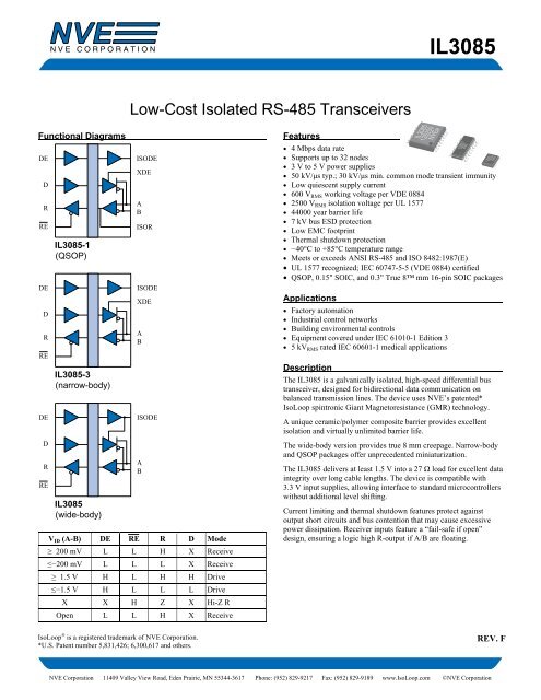
IL3085 Low-Cost Isolated RS-485 Transceiver ... - NVE Corporation
IL3085 Low-Cost Isolated RS-485 Transceiver ... - NVE Corporation
IL3085 Low-Cost Isolated RS-485 Transceiver ... - NVE Corporation

Create successful ePaper yourself
Turn your PDF publications into a flip-book with our unique Google optimized e-Paper software.
<strong>IL3085</strong>Absolute Maximum Ratings (11)Parameter Symbol Min. Typ. Max. Units Test ConditionsStorage Temperature T S −55 150 °CJunction Temperature T J −55 150 °CAmbient Operating Temperature T A −40 85 °CVoltage Range at A or B Bus Pins −8 12.5 VSupply Voltage (1) V DD1 , V DD2 −0.5 7 VDigital Input Voltage −0.5 V DD + 0.5 VDigital Output Voltage −0.5 V DD + 1 VESD (all bus nodes) 7 kV HBMRecommended Operating ConditionsParameter Symbol Min. Typ. Max. Units Test ConditionsVSupply VoltageDD13.05.5VV DD24.55.5Junction Temperature T J −40 100 °CInput Voltage at any Bus Terminal12V(separately or common mode)−7V IV ICHigh-Level Digital Input VoltageV IH2.43.0V DD1 V<strong>Low</strong>-Level Digital Input Voltage V IL 0 0.8 VDifferential Input Voltage (2) V ID +12 / −7 VHigh-Level Output Current (Driver) I OH 60 mAHigh-Level Digital Output Current(Receiver)I OH 8 mA<strong>Low</strong>-Level Output Current (Driver) I OL −60 mA<strong>Low</strong>-Level Digital Output Current(Receiver)I OL −8 mAAmbient Operating Temperature T A −40 85 °CDigital Input Signal Rise and Fall Times t IR , t IF DC StableV DD1 = 3.3 VV DD1 = 5.0 VInsulation SpecificationsParameter Symbol Min. Typ. Max. Units Test Conditions<strong>IL3085</strong>-1E3.2Creepage Distance<strong>IL3085</strong>-3E4.0mm(external)<strong>IL3085</strong>E8.03 8.3Per IEC 60601Total Barrier Thickness (internal) 0.012 0.013 mmBarrier Resistance R IO >10 14 Ω 500 VBarrier Capacitance C IO 7 pF f = 1 MHzLeakage Current 0.2 μA RMS 240 V RMS , 60 HzComparative Tracking Index CTI ≥175 V Per IEC 60112High Voltage Endurance AC1000V RMS(Maximum Barrier VoltageV IOfor Indefinite Life)DC1500Barrier Life 44000 YearsV DCAt maximumoperating temperature100°C, 1000 V RMS , 60%CL activation energyThermal CharacteristicsParameter Symbol Min. Typ. Max. Units Test ConditionsQSOP60Junction–Ambient0.15" SOIC θThermal ResistanceJA600.3" SOIC60°C/WJunction–Case (Top)Thermal ResistancePower DissipationQSOP0.15" SOIC0.3" SOICQSOP0.15" SOIC0.3" SOICΨ JTP D101020675700800°C/WmWSoldered to doublesidedboard;free air2<strong>NVE</strong> <strong>Corporation</strong> 11409 Valley View Road, Eden Prairie, MN 55344-3617 Phone: (952) 829-9217 Fax: (952) 829-9189 www.IsoLoop.com ©<strong>NVE</strong> <strong>Corporation</strong>
<strong>IL3085</strong>Safety and ApprovalsIEC 60747-5-5 (VDE 0884) (File Number 5016933-4880-0001 for SOICs)• Working Voltage (V IORM ) 600 V RMS (848 V PK ); basic insulation; pollution degree 2• Transient overvoltage (V IOTM ) and surge voltage (V IOSM ) 4000 V PK• Each part tested at 1590 V PK for 1 second, 5 pC partial discharge limit• Samples tested at 4000 V PK for 60 sec.; then 1358 V PK for 10 sec. with 5 pC partial discharge limit• QSOP approval pendingSafety-Limiting Values Symbol Value UnitsSafety rating ambient temperature T S 180 °CSafety rating power (180°C) P S 270 mWSupply current safety rating (total of supplies) I S 54 mAIEC 61010-1 (Edition 2; TUV Certificate Numbers N1502812; N1502812-101)Reinforced Insulation; Pollution Degree II; Material Group IIIPart No. Suffix Package Working Voltage-1 QSOP 150 V RMS-3 SOIC 150 V RMSNone True 8 Wide-body SOIC 300 V RMSUL 1577 (Component Recognition Program File Number E207481)Each part tested at 3000 V RMS (4240 V PK ) for 1 second; each lot sample tested at 2500 V RMS (3530 V PK ) for 1 minuteSoldering ProfilePer JEDEC J-STD-020C, MSL 13<strong>NVE</strong> <strong>Corporation</strong> 11409 Valley View Road, Eden Prairie, MN 55344-3617 Phone: (952) 829-9217 Fax: (952) 829-9189 www.IsoLoop.com ©<strong>NVE</strong> <strong>Corporation</strong>
<strong>IL3085</strong><strong>IL3085</strong>-1 (QSOP Package) Pin Connections1 V DD1 Input power supply2 R Output data from bus3 GND 1 Input power supply ground return4 RERead data enable(if RE is high, R= high impedance)5 DE Drive enable6 D Data input to bus7, 8 NC No internal connection9 A Non-inverting bus line10 B Inverting bus lineOutput transceiver power supply11 V DD2X(normally connected to pin 16)<strong>Transceiver</strong> Device Enable input enables thetransceiver from the bus side, or is12 XDE connected to ISODE to enable the transceiverfrom the controller-side DE input.(this input should not be left unterminated)<strong>Isolated</strong> R output13 ISOR (for testing; no connection should be madeto this pin)14 GND 2 Output power supply ground return.15 ISODE<strong>Isolated</strong> DE output(normally connected to pin 12)Output isolation power supply16 V DD2I(normally connected to pin 11)V DD1RGND 1REDEDNCNC12345678<strong>IL3085</strong>-1161514131211109V DD2ISODEGND 2ISORXDEV DD2XBA<strong>IL3085</strong>-3 (0.15" SOIC Package) Pin Connections1 V DD1 Input power supply2 GND 1 Input power supply ground return3 R Output data from bus4 RERead data enable(if RE is high, R= high impedance)5 D Data input to bus6 DE Drive enable7, 8, 9 NC No internal connection10 XDE<strong>Transceiver</strong> Device Enable input enables thetransceiver from the bus side, or isconnected to ISODE to enable the transceiverfrom the controller-side DE input.(this input should not be left unterminated)11 A Non-inverting bus line12 B Inverting bus lineOutput transceiver power supply13 V DD2X(normally connected to pin 16)14 ISODE<strong>Isolated</strong> DE output(normally connected to pin 10)15 GND 2 Output power supply ground return.Output isolation power supply16 V DD2I(normally connected to pin 13)4VDD 1GND 1RREDDENCNC12345678<strong>IL3085</strong>-3161514131211109VDD 2IGND 2ISODEVDD 2XBAXDENC<strong>NVE</strong> <strong>Corporation</strong> 11409 Valley View Road, Eden Prairie, MN 55344-3617 Phone: (952) 829-9217 Fax: (952) 829-9189 www.IsoLoop.com ©<strong>NVE</strong> <strong>Corporation</strong>
<strong>IL3085</strong><strong>IL3085</strong> (0.3" SOIC Package) Pin Connections1 V DD1 Input power supplyInput power supply ground return2 GND 1(pin 2 is internally connected to pin 8)3 R Output data from bus4 RERead data enable(if RE is high, R= high impedance)5 DE Drive enable6 D Data input to bus7 NC No internal connectionInput power supply ground return8 GND 1(pin 8 is internally connected to pin 2)Output power supply ground return9 GND 2(pin 9 is internally connected to pin 15)<strong>Isolated</strong> DE output for use in PROFIBUS10 ISODE applications where the state of the isolateddrive enable node needs to be monitored.11 NC No internal connection12 A Non-inverting bus line13 B Inverting bus line14 NC No internal connectionOutput power supply ground return15 GND 2(pin 15 is internally connected to pin 9)16 V DD2 Output power supplyVDD 1116 VDD 2GND 1215 GND 2R 314 NCRE 413 BDE 512 ADNC671110NCISODEGND 189 GND 2<strong>IL3085</strong>5<strong>NVE</strong> <strong>Corporation</strong> 11409 Valley View Road, Eden Prairie, MN 55344-3617 Phone: (952) 829-9217 Fax: (952) 829-9189 www.IsoLoop.com ©<strong>NVE</strong> <strong>Corporation</strong>
<strong>IL3085</strong>Driver SectionElectrical Specifications (T min to T max and V DD = 4.5 V to 5.5 V unless otherwise stated)Parameter Symbol Min. Typ. (5) Max. Units Test ConditionsOutput voltage V O V DD V I O = 0Differential Output Voltage (2) |V OD1 | V DD V I O = 0Differential Output Voltage (2, 6) V OD3 1.5 2.3 5 V R L = 27 Ω, V DD = 4.5 VChange in Magnitude of DifferentialOutput Voltage (7) Δ|V OD | ±0.01 ±0.2 V R L = 27 Ω or 50 ΩCommon Mode Output Voltage V OC 3 V R L = 27 Ω or 50 ΩChange in Magnitude of CommonMode Output Voltage (7) Δ|V OC | ±0.01 ±0.2 V R L = 27 Ω or 50 ΩOutput Current (4)1Output Disabled, VI OmAO = 12−0.8V O = −7High Level Input Current I IH 10 μA V I = 3.5 V<strong>Low</strong> Level Input Current I IL −10 μA V I = 0.4 VAbsolute |Short-circuit Output Current| I OS 250 mA −7 V < V O < 12 VSupply CurrentV DD1 = 5 VI DD146No LoadmAV DD1 = 3.3 VI DD1 34(Outputs Enabled)Notes (apply to both driver and receiver sections):1. All voltages are with respect to network ground except differential I/O bus voltages.2. Differential input/output voltage is measured at the noninverting terminal A with respect to the inverting terminal B.3. Skew limit is the maximum propagation delay difference between any two devices at 25°C.4. The power-off measurement in ANSI Standard EIA/TIA-422-B applies to disabled outputs only and is not applied to combined inputs andoutputs.5. All typical values are at V DD1 ,V DD2 = 5 V or V DD1 = 3.3 V and T A = 25°C.6. −7 V < V CM < 12 V; 4.5 V < V DD < 5.5 V.7. Δ|V OD | and Δ|V OC | are the changes in magnitude of V OD and V OC , respectively, that occur when the input is changed from one logic state tothe other.8. This applies for both power on and power off, refer to ANSI standard <strong>RS</strong>-<strong>485</strong> for exact condition. The EIA/TIA-422-B limit does not applyfor a combined driver and receiver terminal.9. Includes 10 ns read enable time. Maximum propagation delay is 25 ns after read assertion.10. Pulse skew is defined as |t PLH – t PHL | of each channel.11. Absolute Maximum specifications mean the device will not be damaged if operated under these conditions. It does not guaranteeperformance.12. The relevant test and measurement methods are given in the Electromagnetic Compatibility section on p. 6.13. External magnetic field immunity is improved by this factor if the field direction is “end-to-end” rather than to “pin-to-pin” (see diagram on p. 6).6<strong>NVE</strong> <strong>Corporation</strong> 11409 Valley View Road, Eden Prairie, MN 55344-3617 Phone: (952) 829-9217 Fax: (952) 829-9189 www.IsoLoop.com ©<strong>NVE</strong> <strong>Corporation</strong>
<strong>IL3085</strong>Receiver SectionParameterElectrical Specifications (T min to T max and V DD = 4.5 V to 5.5 V unless otherwise stated)Symbol Min. Typ. (5) Max. Units Test ConditionsPositive-going Input ThresholdVoltageV IT+ 0.2 V −7 V < V CM < 12 VNegative-going Input ThresholdVoltageV IT− −0.2 V −7 V < V CM < 12 VHysteresis Voltage (V IT+ − V IT− ) V HYS 70 mV V CM = 0 V, T = 25°CHigh Level Digital Output Voltage V OH V DD – 0.2 V DD VV ID = 200 mVI OH = −20 μA<strong>Low</strong> Level Digital Output Voltage V OL 0.2 VV ID = −200 mVI OH = 20 μAHigh-impedance-state output current I OZ ±1 μA V O = 0.4 to (V DD2 −0.5) VLine Input Current (8) I I 1 mA V I = 12 V−0.8 mA V I = −7 VInput Resistance R I 12 kΩSupply Current I DD2 5 16 mANo load; OutputsEnabled; V DD2Xconnected to V DD2I ifapplicableSwitching CharacteristicsParameterV DD1 = 5 V, V DD2 = 5 VSymbol Min. Typ. (5) Max. Units Test ConditionsData Rate 4 Mbps R L = 54 Ω, C L = 50 pFPropagation Delay (2, 9) t PD 48 150 nsV O = −1.5 to 1.5 V,C L = 15 pFPulse Skew (2, 10) t SK (P) 6 15 nsV O = −1.5 to 1.5 V,C L = 15 pFOutput Enable Time To High Level t PZH 33 50 ns C L = 15 pFOutput Enable Time To <strong>Low</strong> Level t PZL 33 50 ns C L = 15 pFOutput Disable Time From High Level t PHZ 33 50 ns C L = 15 pFOutput Disable Time From <strong>Low</strong> Level t PLZ 33 50 ns C L = 15 pFCommon Mode Transient Immunity|CM(Output Logic High to Logic <strong>Low</strong>)H |,|CM L | 30 50 kV/μsV CM = 1500 V DCt TRANSIENT = 25 nsV DD1 = 3.3 V, V DD2 = 5 VParameter Symbol Min. Typ. (5) Max. Units Test ConditionsData Rate 4 Mbps R L = 54 Ω, C L = 50 pFPropagation Delay (2, 9) t PD 48 150 nsPulse Skew (2, 10) t SK (P) 6 20 nsV O = −1.5 to 1.5 V,C L = 15 pFV O = −1.5 to 1.5 V,C L = 15 pFOutput Enable Time To High Level t PZH 33 50 ns C L = 15 pFOutput Enable Time To <strong>Low</strong> Level t PZL 33 50 ns C L = 15 pFOutput Disable Time From HighLevelt PHZ 33 50 ns C L = 15 pFOutput Disable Time From <strong>Low</strong> Level t PLZ 33 50 ns C L = 15 pFCommon Mode Transient Immunity(Output Logic High to Logic <strong>Low</strong>)|CM H |,|CM L | 30 50 kV/μsV CM = 1500 V DCt TRANSIENT = 25 ns7<strong>NVE</strong> <strong>Corporation</strong> 11409 Valley View Road, Eden Prairie, MN 55344-3617 Phone: (952) 829-9217 Fax: (952) 829-9189 www.IsoLoop.com ©<strong>NVE</strong> <strong>Corporation</strong>
<strong>IL3085</strong>Magnetic Field Immunity (12)V DD1 = 5 V, V DD2 = 5 VPower Frequency Magnetic Immunity H PF 2800 3500 A/m 50Hz/60HzPulse Magnetic Field Immunity H PM 4000 4500 A/m t p = 8µsDamped Oscillatory Magnetic Field H OSC 4000 4500 A/m 0.1Hz – 1MHzCross-axis Immunity Multiplier (13) K X 2.5V DD1 = 3.3 V, V DD2 = 5 VPower Frequency Magnetic Immunity H PF 1000 1500 A/m 50Hz/60HzPulse Magnetic Field Immunity H PM 1800 2000 A/m t p = 8µsDamped Oscillatory Magnetic Field H OSC 1800 2000 A/m 0.1Hz – 1MHzCross-axis Immunity Multiplier (13) K X 2.58<strong>NVE</strong> <strong>Corporation</strong> 11409 Valley View Road, Eden Prairie, MN 55344-3617 Phone: (952) 829-9217 Fax: (952) 829-9189 www.IsoLoop.com ©<strong>NVE</strong> <strong>Corporation</strong>
<strong>IL3085</strong>Electrostatic Discharge SensitivityThis product has been tested for electrostatic sensitivity to the limits stated in the specifications. However, <strong>NVE</strong> recommends that all integratedcircuits be handled with appropriate care to avoid damage. Damage caused by inappropriate handling or storage could range from performancedegradation to complete failure.Pinout Differences Between PackagesQSOP and narrow-body version (<strong>IL3085</strong>-1E and <strong>IL3085</strong>-3E) are designed for application flexibility and minimum board area in dense PCAs.The wide-body version (<strong>IL3085</strong>E) has redundant ground pins for layout flexibility.QSOP and narrow-body versions provide separate isolated DE output (ISODE) and <strong>Transceiver</strong> Device Enable (XDE) input. ISODE follows theDevice Enable input (DE). XDE can be used to enable and disable the transceiver from the bus side, or connected to ISODE to enable and disablethe transceiver from the DE controller-side input. The QSOP and narrow-body versions also provide separate bus-side power supply pins—V DD2X for the transceiver module and V DD2I for the isolation module. These should be externally connected for normal operation, but can be usedseparately for testing or troubleshooting. The QSOP version also has an “ISOR” output that is isolated with respect to the controller-side “R.”This pin is used for testing and normally not connected, but could be used for a bus-side data output under special circumstances.The wide-body version has internal connections between the isolated DE output and the <strong>Transceiver</strong> Device Enable input, and well as betweenthe two V DD2 bus-side power supply pins. The two internally-connected GND pins for each supply side provide layout flexibility. The ISODEoutput can be used in PROFIBUS applications where the state of the isolated drive enable node needs to be monitored, or for testing ortroubleshooting.Dynamic Power ConsumptionIsoLoop Isolators have low power consumption because data is transmitted across the isolation barrier only on edge transitions. Powerconsumption therefore varies with the data rate. Typical dynamic supply currents are as follows:Data Rate (Mbps) I DD1 I DD21 150 μA 150 μA4 600 μA 600 μATable 2. Typical Dynamic Supply Currents.Power Supply DecouplingBoth V DD1 and V DD2 must be bypassed with 47 nF ceramic capacitors. These should be placed as close as possible to V DD pins for properoperation. Additionally, V DD2 should be bypassed with a 10 µF tantalum capacitor.Maintaining CreepageCreepage distances are often critical in isolated circuits. In addition to meeting JEDEC standards, <strong>NVE</strong> isolator packages have unique creepagespecifications. Standard pad libraries often extend under the package, compromising creepage and clearance. Similarly, ground planes, if used,should be spaced to avoid compromising clearance. Package drawings and recommended pad layouts are included in this datasheet.DC CorrectnessThe <strong>IL3085</strong> incorporates a patented refresh circuit to maintain the correct output state with respect to data input. At power up, the bus outputswill follow the Function Table shown on Page 1. The DE input should be held low during power-up to eliminate false drive data pulses from thebus. An external power supply monitor to minimize glitches caused by slow power-up and power-down transients is not required.Electromagnetic CompatibilityThe <strong>IL3085</strong> is fully compliant with generic EMC standards EN50081, EN50082-1 and the umbrella line-voltage standard for InformationTechnology Equipment (ITE) EN61000. The IsoLoop Isolator’s Wheatstone bridge configuration and differential magnetic field signaling ensureexcellent EMC performance against all relevant standards. <strong>NVE</strong> conducted compliance tests in the categories below:EN50081-1Residential, Commercial & Light IndustrialMethods EN55022, EN55014EN50082-2: Industrial EnvironmentMethods EN61000-4-2 (ESD), EN61000-4-3 (Electromagnetic Field Immunity), EN61000-4-4 (Electrical Transient Immunity),EN61000-4-6 (RFI Immunity), EN61000-4-8 (Power Frequency Magnetic Field Immunity)ENV50204Radiated Field from Digital Telephones (Immunity Test)Immunity to external magnetic fields is even higher if the field direction is “end-to-end” (rather than to “pin-to-pin”) as shown above.9<strong>NVE</strong> <strong>Corporation</strong> 11409 Valley View Road, Eden Prairie, MN 55344-3617 Phone: (952) 829-9217 Fax: (952) 829-9189 www.IsoLoop.com ©<strong>NVE</strong> <strong>Corporation</strong>
<strong>IL3085</strong>Application InformationFigures 1a, 1b, and 1c show typical connections to a bus and microcontroller for the three package versions. The schematics include typicaltermination and fail-safe resistors, and power supply decoupling capacitors:VDD1 = 3.3 VVDD2 = 5 VC DD147nF1<strong>IL3085</strong>-111 16C DD2BC DD2 +47nF 10µFDE515 ISODEMicrocontrollerDRRE624GND13 14IsolationBoundary12XDE910ISOR13GND2R FS-EXT560RR T120RR FS-EXT560RFigure 1a. Typical QSOP transceiver connections.ABVDD1 = 3.3 VVDD2 = 5 VC DD147nF1<strong>IL3085</strong>-313 16C DD2BC DD2 +47nF 10µFDE614 ISODEMicrocontrollerDRRE53410XDE1112R FS-EXT560RR T120RAB2 15IsolationBoundaryGND1GND2Figure 1b. Typical narrow-body connections.R FS-EXT560RVDD1 = 3.3 VVDD2 = 5 VC DD147nF1<strong>IL3085</strong>16C DD2 +47nF 10µFC DD2BMicrocontrollerDEDRRE563410ISODE1213R FS-EXT560RR T120RAB2 or 8 9 or 15IsolationBoundaryGND1GND2Figure 1c. Typical wide-body connections.R FS-EXT560R10<strong>NVE</strong> <strong>Corporation</strong> 11409 Valley View Road, Eden Prairie, MN 55344-3617 Phone: (952) 829-9217 Fax: (952) 829-9189 www.IsoLoop.com ©<strong>NVE</strong> <strong>Corporation</strong>
<strong>IL3085</strong>Receiver FeaturesThe receiver output “R” has tri-state capability via the active low RE input.Driver FeaturesThe <strong>RS</strong>-<strong>485</strong> driver has a differential output and delivers at least 2.1 V across a 54 Ω load. Drivers feature low propagation delay skew tomaximize bit width and minimize EMI. Drivers have tri-state capability via the active-high DE input.Receiver Data Rate, Cables and TerminationsThe <strong>IL3085</strong> is intended for networks up to 4,000 feet (1,200 m), but the maximum data rate decreases as cable length increases. Twisted paircable should be used in all networks since they tend to pick up noise and other electromagnetically induced voltages as common mode signals,which are effectively rejected by the differential receiver.Fail-Safe Operation“Fail-safe operation” is defined here as the forcing of a logic high state on the “R” output in response to an open-circuit condition between the“A” and “B” lines of the bus, or when no drivers are active on the bus.Proper biasing can ensure fail-safe operation, that is a known state when there are no active drivers on the bus. IL3000-Series <strong>Isolated</strong><strong>Transceiver</strong>s include internal pull-up and pull-down resistors of approximately 30 kΩ in the receiver section (R FS-INT ; see figure below). Theseinternal resistors are designed to ensure failsafe operation but only if there are no termination resistors. The entire V DD will appear between inputs“A” and “B” if there is no loading and no termination resistors, and there will be more than the required 200 mV with up to four <strong>RS</strong>-<strong>485</strong> worstcaseUnit Loads of 12 kΩ. Many designs operating below 1 Mbps or less than 1,000 feet are unterminated. Termination resistors may not benecessary for very low data rates and very short cable runs because reflections have time to settle before data sampling, which occurs at themiddle of the bit interval.In busses with low-impedance termination resistors however, the differential voltage across the conductor pair will be close to zero with no activedrivers. In this case the state of the bus is indeterminate, and the idle bus will be susceptible to noise. For example, with 120 Ω terminationresistors (R T ) on each end of the cable, and four Unit Loads (12 kΩ each), without external fail-safe biasing resistors the internal pull-up and pulldownresistors will produce a voltage between inputs “A” and “B” of only about 5 mV. This is not nearly enough to ensure a known state.External fail-safe biasing resistors (R FS-EXT ) at one end of the bus can ensure fail-safe operation with a terminated bus. Resistors should beselected so that under worst-case power supply and resistor tolerances there is at least 200 mV across the conductor pair with no active drivers tomeet the input sensitivity specification of the <strong>RS</strong>-<strong>485</strong> standard.Using the same value for pull-up and pull-down biasing resistors maintains balance for positive- and negative going transitions. <strong>Low</strong>er-valueresistors increase inactive noise immunity at the expense of quiescent power consumption. Note that each Unit Load on the bus adds a worst-caseloading of 12 kΩ across the conductor pair, and 32 Unit Loads add 375 Ω worst-case loading. The more loads on the bus, the lower the requiredvalues of the biasing resistors.In the example with two 120 Ω termination resistors and four Unit Loads, 560 Ω external biasing resistors provide more than 200 mV between“A” and “B” with adequate margin for power supply variations and resistor tolerances. This ensures a known state when there are no activedrivers. Other illustrative examples are shown in the following table:11<strong>NVE</strong> <strong>Corporation</strong> 11409 Valley View Road, Eden Prairie, MN 55344-3617 Phone: (952) 829-9217 Fax: (952) 829-9189 www.IsoLoop.com ©<strong>NVE</strong> <strong>Corporation</strong>
<strong>IL3085</strong>Fail-Safe Biasing5 VRV DDRFS-INT RFS-INTGND30K 30KABRFS-EXTRFS-EXTRTRTNominal V A-B Fail-SafeR FS-EXT R T Loading (inactive) Operation?Internal Only None Four unit loads (12 kΩ ea.) 238 mV YesInternal Only 120 Ω Four unit loads (12 kΩ ea.) 5 mV No560 Ω 120 Ω Four unit loads (12 kΩ ea.) 254 mV Yes510 Ω 120 Ω 32 unit loads (12 kΩ ea.) 247 mV Yes12<strong>NVE</strong> <strong>Corporation</strong> 11409 Valley View Road, Eden Prairie, MN 55344-3617 Phone: (952) 829-9217 Fax: (952) 829-9189 www.IsoLoop.com ©<strong>NVE</strong> <strong>Corporation</strong>
<strong>IL3085</strong>Package DrawingsUltraminiature 16-pin QSOP Package (-1 suffix)Dimensions in inches (mm); scale = approx. 5X0.188 (4.77)0.197 (5.00)0.020 (0.50)0.029 (0.75)0.228 (5.8)0.244 (6.2)0.013 (0.3)0.020 (0.5)0.150 (3.8)0.157 (4.0)NOM0.007 (0.20)0.010 (0.25)0.050 (1.27)0.056 (1.42)0.025 (0.635)0.004 (0.10)0.010 (0.25)NOTE: Pin spacing is a BASICdimension; tolerancesdo not accumulate0.060 (1.52)0.069 (1.75)0.15" 16-pin SOIC Package (-3 suffix)Dimensions in inches (mm); scale = approx. 5X0.013 (0.3)0.020 (0.5)NOM0.386 (9.8)0.394 (10.0)0.007 (0.2)0.013 (0.3)0.016 (0.4)0.050 (1.3)Pin 1 identifiedby either anindent or amarked dot0.055 (1.40)0.062 (1.58)0.054 (1.4)0.072 (1.8)0.150 (3.81)0.157 (3.99)0.228 (5.8)0.244 (6.2)0.049 (1.24)0.051 (1.30)NOTE: Pin spacing is a BASICdimension; tolerancesdo not accumulate0.004 (0.1)0.012 (0.3)13<strong>NVE</strong> <strong>Corporation</strong> 11409 Valley View Road, Eden Prairie, MN 55344-3617 Phone: (952) 829-9217 Fax: (952) 829-9189 www.IsoLoop.com ©<strong>NVE</strong> <strong>Corporation</strong>
<strong>IL3085</strong>0.3" 16-pin SOIC Package (no suffix)Dimensions in inches (mm); scale = approx. 5X0.033 (0.85)*0.043 (1.10)0.260 (6.60)*0.280 (7.11)0.013 (0.3)0.020 (0.5)0.397 (10.08)0.413 (10.49)0.007 (0.2)0.013 (0.3)0.007 (0.18)*0.010 (0.25)0.016 (0.4)0.050 (1.3)0.017 (0.43)*0.022 (0.56)Pin 1 identified byeither an indentor a marked dot0.08 (2.0)0.10 (2.5)0.092 (2.34)0.105 (2.67)0.292 (7.42)*0.299 (7.59)0.394 (10.00)0.419 (10.64)*Specified for True 8 package to guarantee 8 mm creepage per IEC 60601.0.049 (1.24)0.051 (1.30)NOTE: Pin spacing is a BASICdimension; tolerancesdo not accumulate0.004 (0.1)0.012 (0.3)14<strong>NVE</strong> <strong>Corporation</strong> 11409 Valley View Road, Eden Prairie, MN 55344-3617 Phone: (952) 829-9217 Fax: (952) 829-9189 www.IsoLoop.com ©<strong>NVE</strong> <strong>Corporation</strong>
<strong>IL3085</strong>Recommended Pad Layouts4 mm x 5 mm 16-pin QSOP Pad LayoutDimensions in inches (mm); scale = approx. 5X0.160 (4.05)0.025 (0.635)0.012 (0.30)16 PLCS0.275 (6.99)0.15" 16-pin SOIC Pad LayoutDimensions in inches (mm); scale = approx. 5X0.160 (4.06)0.050 (1.27)0.020 (0.51)16 PLCS0.275 (6.99)15<strong>NVE</strong> <strong>Corporation</strong> 11409 Valley View Road, Eden Prairie, MN 55344-3617 Phone: (952) 829-9217 Fax: (952) 829-9189 www.IsoLoop.com ©<strong>NVE</strong> <strong>Corporation</strong>
<strong>IL3085</strong>0.3" 16-pin SOIC Pad LayoutDimensions in inches (mm); scale = approx. 5X0.317 (8.05)0.050 (1.27)0.020 (0.51)16 PLCS0.449 (11.40)16<strong>NVE</strong> <strong>Corporation</strong> 11409 Valley View Road, Eden Prairie, MN 55344-3617 Phone: (952) 829-9217 Fax: (952) 829-9189 www.IsoLoop.com ©<strong>NVE</strong> <strong>Corporation</strong>
<strong>IL3085</strong>Ordering Information and Valid Part NumbersIL 30 85 -3 E TR13Bulk PackagingBlank = TubeTR7 = 7'' Tape and ReelTR13 = 13'' Tape and ReelPackageE = RoHS CompliantPackage TypeBlank = 0.3'' SOIC-3 = 0.15'' SOIC-1 = 0.15'' QSOPValid Part Numbers<strong>IL3085</strong>E<strong>IL3085</strong>E TR13<strong>IL3085</strong>-3E<strong>IL3085</strong>-3E TR7<strong>IL3085</strong>-3E TR13<strong>IL3085</strong>-1E<strong>IL3085</strong>-1E TR7<strong>IL3085</strong>-1E TR13Channel Configuration85 = <strong>RS</strong>-<strong>485</strong>Base Part Number30 = Digital-In, 4 Mbps <strong>Transceiver</strong>Product FamilyIL = IsolatorsRoHSCOMPLIANT17<strong>NVE</strong> <strong>Corporation</strong> 11409 Valley View Road, Eden Prairie, MN 55344-3617 Phone: (952) 829-9217 Fax: (952) 829-9189 www.IsoLoop.com ©<strong>NVE</strong> <strong>Corporation</strong>
<strong>IL3085</strong>Revision HistoryISB-DS-001-<strong>IL3085</strong>-FJune 2014Change• Increased <strong>IL3085</strong>-1E (QSOP) creepage specification from 2.75 mm to 3.2 mm (p. 2).ISB-DS-001-<strong>IL3085</strong>-EChange• Added QSOP version (-1 suffix).• Revised and added details to thermal characteristic specifications (p. 2).• Added VDE 0884 Safety-Limiting Values (p. 3).ISB-DS-001-<strong>IL3085</strong>-DChange• IEC 60747-5-5 (VDE 0884) certification.• Upgraded from MSL 2 to MSL 1.ISB-DS-001-<strong>IL3085</strong>-CChange• Increased transient immunity specifications based on additional data.• Noted UL 1577 recognition, IEC 61010-1 approval, and VDE 0884 pending.• Added transient immunity specifications.• Added high voltage endurance specification.• Increased magnetic immunity specifications.• Updated package outline drawings and added recommended solder pad dimensions.ISB-DS-001-<strong>IL3085</strong>-BJanuary 2013Change• Added thermal characteristics (p. 2).• Finalized maximum data rate (4 Mbps).• Cosmetic changes.ISB-DS-001-<strong>IL3085</strong>-ADecember 2012Change• Initial Release.18<strong>NVE</strong> <strong>Corporation</strong> 11409 Valley View Road, Eden Prairie, MN 55344-3617 Phone: (952) 829-9217 Fax: (952) 829-9189 www.IsoLoop.com ©<strong>NVE</strong> <strong>Corporation</strong>
<strong>IL3085</strong>Datasheet LimitationsThe information and data provided in datasheets shall define the specification of the product as agreed between <strong>NVE</strong> and its customer, unless <strong>NVE</strong> andcustomer have explicitly agreed otherwise in writing. All specifications are based on <strong>NVE</strong> test protocols. In no event however, shall an agreement bevalid in which the <strong>NVE</strong> product is deemed to offer functions and qualities beyond those described in the datasheet.Limited Warranty and LiabilityInformation in this document is believed to be accurate and reliable. However, <strong>NVE</strong> does not give any representations or warranties, expressed orimplied, as to the accuracy or completeness of such information and shall have no liability for the consequences of use of such information.In no event shall <strong>NVE</strong> be liable for any indirect, incidental, punitive, special or consequential damages (including, without limitation, lost profits, lostsavings, business interruption, costs related to the removal or replacement of any products or rework charges) whether or not such damages are based ontort (including negligence), warranty, breach of contract or any other legal theory.Right to Make Changes<strong>NVE</strong> reserves the right to make changes to information published in this document including, without limitation, specifications and product descriptionsat any time and without notice. This document supersedes and replaces all information supplied prior to its publication.Use in Life-Critical or Safety-Critical ApplicationsUnless <strong>NVE</strong> and a customer explicitly agree otherwise in writing, <strong>NVE</strong> products are not designed, authorized or warranted to be suitable for use in lifesupport, life-critical or safety-critical devices or equipment. <strong>NVE</strong> accepts no liability for inclusion or use of <strong>NVE</strong> products in such applications and suchinclusion or use is at the customer’s own risk. Should the customer use <strong>NVE</strong> products for such application whether authorized by <strong>NVE</strong> or not, thecustomer shall indemnify and hold <strong>NVE</strong> harmless against all claims and damages.ApplicationsApplications described in this datasheet are illustrative only. <strong>NVE</strong> makes no representation or warranty that such applications will be suitable for thespecified use without further testing or modification.Customers are responsible for the design and operation of their applications and products using <strong>NVE</strong> products, and <strong>NVE</strong> accepts no liability for anyassistance with applications or customer product design. It is customer’s sole responsibility to determine whether the <strong>NVE</strong> product is suitable and fit forthe customer’s applications and products planned, as well as for the planned application and use of customer’s third party customers. Customers shouldprovide appropriate design and operating safeguards to minimize the risks associated with their applications and products.<strong>NVE</strong> does not accept any liability related to any default, damage, costs or problem which is based on any weakness or default in the customer’sapplications or products, or the application or use by customer’s third party customers. The customer is responsible for all necessary testing for thecustomer’s applications and products using <strong>NVE</strong> products in order to avoid a default of the applications and the products or of the application or use bycustomer’s third party customers. <strong>NVE</strong> accepts no liability in this respect.Limiting ValuesStress above one or more limiting values (as defined in the Absolute Maximum Ratings System of IEC 60134) will cause permanent damage to thedevice. Limiting values are stress ratings only and operation of the device at these or any other conditions above those given in the recommendedoperating conditions of the datasheet is not warranted. Constant or repeated exposure to limiting values will permanently and irreversibly affect thequality and reliability of the device.Terms and Conditions of SaleIn case an individual agreement is concluded only the terms and conditions of the respective agreement shall apply. <strong>NVE</strong> hereby expressly objects toapplying the customer’s general terms and conditions with regard to the purchase of <strong>NVE</strong> products by customer.No Offer to Sell or LicenseNothing in this document may be interpreted or construed as an offer to sell products that is open for acceptance or the grant, conveyance or implicationof any license under any copyrights, patents or other industrial or intellectual property rights.Export ControlThis document as well as the items described herein may be subject to export control regulations. Export might require a prior authorization from national authorities.Automotive Qualified ProductsUnless the datasheet expressly states that a specific <strong>NVE</strong> product is automotive qualified, the product is not suitable for automotive use. It is neitherqualified nor tested in accordance with automotive testing or application requirements. <strong>NVE</strong> accepts no liability for inclusion or use of non-automotivequalified products in automotive equipment or applications.In the event that customer uses the product for design-in and use in automotive applications to automotive specifications and standards, customer (a) shalluse the product without <strong>NVE</strong>’s warranty of the product for such automotive applications, use and specifications, and (b) whenever customer uses theproduct for automotive applications beyond <strong>NVE</strong>’s specifications such use shall be solely at customer’s own risk, and (c) customer fully indemnifies<strong>NVE</strong> for any liability, damages or failed product claims resulting from customer design and use of the product for automotive applications beyond <strong>NVE</strong>’sstandard warranty and <strong>NVE</strong>’s product specifications.19<strong>NVE</strong> <strong>Corporation</strong> 11409 Valley View Road, Eden Prairie, MN 55344-3617 Phone: (952) 829-9217 Fax: (952) 829-9189 www.IsoLoop.com ©<strong>NVE</strong> <strong>Corporation</strong>
<strong>IL3085</strong>An ISO 9001 Certified Company<strong>NVE</strong> <strong>Corporation</strong>11409 Valley View RoadEden Prairie, MN 55344-3617 USATelephone: (952) 829-9217Fax: (952) 829-9189www.nve.come-mail: iso-info@nve.com©<strong>NVE</strong> <strong>Corporation</strong>All rights are reserved. Reproduction in whole or in part is prohibited without the prior written consent of the copyright owner.ISB-DS-001-<strong>IL3085</strong>-F20June 2014<strong>NVE</strong> <strong>Corporation</strong> 11409 Valley View Road, Eden Prairie, MN 55344-3617 Phone: (952) 829-9217 Fax: (952) 829-9189 www.IsoLoop.com ©<strong>NVE</strong> <strong>Corporation</strong>